


Fabrication and properties of silicene and silicene–graphene layered structures on Ir (111)
[Meng Leia), b) , Wang Ye-Liang†b)  , Zhang Li-Zhi
b) , Du Shi-Xuanb) , Gao Hong-Jun‡b) ]
, Zhang Li-Zhi]
|
|


†Corresponding author. E-mail: ylwang@iphy.ac.cn
‡Corresponding author. E-mail: hjgao@iphy.ac.cn
*Project supported by the National Basic Research Program of China (Grant Nos. 2013CBA01600 and 2011CB932700), the National Natural Science Foundation of China (Grant Nos. 61222112, 61390501, 51325204, 11334006, and 61306114), the Science Fund from Chinese Academy of Sciences (Grant Nos. 1731300500015 and XDB07030100), and the Fundamental Research Funds for the Central Universities, China.
Silicene, a two-dimensional (2D) honeycomb structure similar to graphene, has been successfully fabricated on various substrates. This work will mainly review the syntheses and the corresponding properties of silicene and silicene–graphene layered structures on Ir (111) substrates. For silicene on Ir (111), the buckled
Silicene, in which silicon atoms are substituted for carbon atoms in graphene, has recently created considerable interest among scientists. Silicene is expected to have extremely useful physical properties, [1– 16] as a new honeycomb structure similar to that of graphene among two-dimensional (2D) atomic/molecular crystalline materials.[17– 31] Before silicene was conceived as a possible material, theorists and the experimental physicists had already analyzed in some detail very thin and narrow silicon nanostructures/nanowires.[32– 37] Actually silicon strips also have been studied in early experimental stage.[38– 42] Subsequently, theoretical models based on free-standing single-layer silicon and the conception of silicene were considered.[2] As classical and attractive calculations to experimental researchers, Cahangirov et al. proposed that silicon atoms prefer to form a corrugated sheet structure.[3] In addition, the quantum spin Hall effect[5] and chiral superconductivity[43] have been predicted theoretically to be observable on silicene.
The preparation of silicene in experiments is extremely difficult. As is well known, graphene, a flat single layer of sp2-bonded carbon atoms, can be exfoliated from graphite easily because of the weak inter-layer interactions of graphite. However, silicene cannot be exfoliated from bulk silicon because silicon in the bulk is sp3-hybridized. Breaking the covalent Si– Si bonds is too difficult to realize experimentally. Therefore, obtaining a 2D silicon sheet through exfoliation is impossible. Currently, the primary method to fabricate silicene sheets is to epitaxially grow the silicon on solid surfaces. The fabrication of such a sheet was reported on Ag (111) surface, which can form several phases depending on the silicon coverage and substrate temperature.[7, 44– 62] And very recently, a silicene field-effect transistor has also been realized by a growth– transfer– fabrication process based on silicene/Ag (111) system, this work should pave the way to the practical application of silicene in semiconductor technology.[63, 64] Apart from an Ag (111) substrate, silicene has been reported on zirconium diboride (ZrB2) thin films grown on Si wafers.[8] The silicene on ZrB2 is almost consistent with one superstructure of silicene/Ag (111) system.[46] Both studies observed a 
In this paper, we review the geometric and electronic properties of silicene and silicene– graphene layered structures on Ir (111) substrates. For silicene on Ir (111), [73] it shows a 


Until now, silicene has been fabricated on several different substrates, where silicon atoms are prone to form various superstructures depending on the silicon coverage and annealing temperature.[45, 46] In this section, the structural feature and physical behavior of silicene on Ir (111) surface are explored, which is mainly based on the characterization of LEED and STM measurements. Experiments were performed in an ultra-high vacuum (UHV) system with a base pressure of about 2 × 10− 10 mbar (1 mbar = 105 Pa), which provides a great growth condition that prevents silicon from being oxidized. The Ir (111) substrate was cleaned several cycles of sputtering and annealing. The silicon was deposited on Ir (111) at room temperature from a piece of silicon heated by a direct current. After deposition, the sample was annealed at 670 K for 30 min. Then, LEED was employed to identify the superstructures macroscopically and STM to image the surface in atomic scale detail. The density functional theory (DFT)-based first-principles calculations were performed by using the Vienna ab initio simulation package (VASP). The projector augmented wave (PAW) potentials were used to describe the core electrons, and the generalized gradient approximation of Perdew, Burke, and Ernzerhof (PBE) were used for implementing the exchange and correlation. The periodic slab models include four layers of iridium, one layer of silicene, and a 15-Å thick vacuum layer. All atoms were fully relaxed except for the bottom two substrate layers until the net force on every atom was smaller than 0.01 eV/Å . The energy cutoff of the plane-wave basis sets was 250 eV, and the K-point sampling was 9× 9× 1.
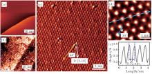
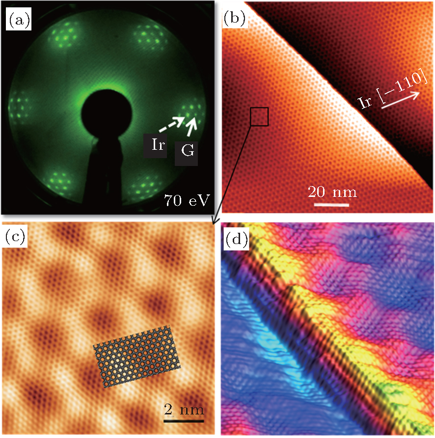
Figure 1(a) displays the LEED pattern in reciprocal space obtained at the prepared Ir (111) surface, showing a distinct Ir (1× 1) diffraction spot, which is assigned to the Ir (111) substrate with six-fold symmetry. For clarity, a sketch map of the diffraction spots in reciprocal space is shown in Fig. 1(b), where the reciprocal vectors of the diffraction spots are indicated by white arrows. Then, after silicon was deposited and annealed, the structural characterization of the silicon layer formed on Ir (111) surface was identified macroscopically by the arising LEED pattern as shown in Fig. 1(c). Apart from the outer six bright spots, the additional distinct diffraction spots then originate from the silicon superstructure. The LEED pattern, with the incident electron beam energy decreasing, allows a clearer imaging of the inner diffraction spots as shown in Fig. 1(d). The sketch map of the diffraction spots of the superstructure (Fig. 1(e)) implies that two symmetrically equivalent domains exist, aside from the (1× 1) diffraction spots of the Ir (111) lattice. The schematic diagram in real space, which is consistent with the diffraction patterns provided in Fig. 1(f), reveals the commensurability relation between the silicon adlayer and the substrate lattice. Thus, the silicon adlayer is identified as a 


 | Fig. 1. LEED patterns and the corresponding schematic diagrams of the Ir (111) surface before and after silicon deposition. (a) The six bright spots originating from the six-fold symmetry of the Ir (111) substrate. (b) Sketch of the diffraction spots shown in panel (a), where the reciprocal vectors are indicated by white arrows. (c) Outer six bright spots (highlighted by the dashed circles), and the additional diffraction spots due to the silicon adlayer. (d) LEED pattern of the silicon superstructure obtained with lower incident electron beam energy. (e) Sketch of the diffraction spots shown in panel (c), where the reciprocal vectors of each group of spots are indicated by white, red, and blue arrows respectively. (f) Schematic diagram of the diffraction spots in real space. These data reveal a  |
Figures 2(a) and 2(b) are the STM images obtained in real space on the Ir (111) surface before and after silicon deposition. The image in Fig. 2(a) indicates the Ir (111) substrate has clean surface terraces before silicon deposition. After silicon deposition, silicon forms amorphous aggregations or silicon clusters on the Ir (111) substrate while the sample is at room temperature (Fig. 2(b)). This phenomenon is similar to that of silicene/Ag (111) system, where different phases of silicene can only be formed above certain substrate temperatures.[46] After sample annealing (670 K), well-ordered structures can be found (Figs. 2(c) and 2(d)), which are obtained in different scanning areas on the same sample surface. The large scale STM image in Fig. 2(c) shows a long-range order of the silicon superstructure. Comparing the directions between the superstructure in Fig. 2(c) and the one in Fig. 2(d), it is noteworthy that they have different orientations with respect to the substrate Ir (111) lattice, with a relative rotation of 22° . This is consistent with the two equivalent domains detected in 


 | Fig. 2. STM images of the Ir (111) surface (a) before (U = − 0.1 V, and I = 0.11 nA) and (b) after (U = − 1.12 V, and I = 0.03 nA) silicon deposition. (c) STM topographic image (U = − 1.45 V, and I = 0.25 nA), showing a  |
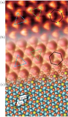
Apart from the brightest protrusions in STM images, there are two other regions showing different image contrasts, marked by upward and downward triangles (Fig. 3(a)), respectively. It is obvious that the region inside the upward triangle is brighter than the one in the downward triangle. Considering the contrast differences in these regions, a honeycomb-like configuration of the silicon superstructure can be proposed and is depicted in Fig. 3(a): the darkest regions are the centers of the honeycomb lattice; the brightest protrusions are the vertexes (indicated by yellow dots) of the honeycomb. This honeycomb-like configuration is, in fact, a superlattice of the silicene structure. According to the prediction of previous theoretical studies, [1, 3, 5] the lattice constant of low-buckled free-standing silicene is about 3.8 Å – 3.9 Å . In that case, the lattice constant of the 


 | Fig. 3. (a) Zoomed-in STM image of the silicon layer. Besides the brightest protrusions, two other regions showing different contrasts are indicated by the upward and downward triangles. The honeycomb feature is indicated by the black hexagon. (b) Simulated STM image, showing features identical with the experimental results in the same triangles and hexagons. (c) Top view of the relaxed atomic model of the   |
DFT calculations and simulations of the STM observations using the Tersoff– Hamann approach[76] provide advanced ways to evaluate the assumption above and to gain a deeper understanding of the silicene/Ir (111) system. Figure 3(b) shows the simulated STM image and the brightest protrusions in the formation of the hexagonal arrangement are indicated. In the simulations there is distinct contrast between the two triangular regions in a unit cell. These features are in excellent consistence with the STM observations in Fig. 3(a), verifying that the model of the 


The relaxed model and the simulated STM image obviously provide a clear picture of the silicon arrangements in the adlayer corresponding to observations in the actual STM images. The silicon atoms at the top sites of the iridium lattice (the yellow balls in Figs. 3(b) and 3(c)) correspond to the brightest protrusions (every other vertex of the honeycomb feature) exhibited in the STM image (Fig. 3(a)). The less bright protrusion in the center of the upward triangle region (the other three vertexes) can be explained as the silicon atoms at fcc hollow sites, showing lower electron density of states than density of the silicon atoms atop sites. The dim region in the center of the downward triangular region features the silicon atoms located at the hcp hollow sites with the lowest electron density of states. The calculation results show that the silicon atoms are located at two different heights with respect to the substrate: the distance between the top silicon atoms (yellow balls) and the iridium substrate is about 2.83 Å , and the distance between the other silicon atoms (orange balls) and the substrate is around 2 Å . This height difference (0.83 Å ) is to some degree consistent with the reported results of silicon sheets on Ag (111), where the height difference is 0.75 Å .[7] The undulation clearly reveals an undulated silicon layer on Ir (111).
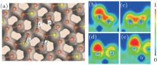
A key issue is about the continuity of silicon layer, since a buckled structure with an undulation in the silicon layer implies an interaction between silicon layer and the substrate. The continuity of silicon layer may be influenced if such an interaction is strong. Thus it is very important to testify that the silicon layer is a continuous layer rather than an accumulation of fragments with several silicon atoms. To prove this argument, it is needed to establish that the interactions between silicon atoms in the sheet are much stronger than those of silicon atoms with the underlying substrate. The electron localization function (ELF) can be used to analyze these interactions, which directly allows one to gauge chemical interactions from the charge localization between individual atoms.[77, 78] The value of the ELF can be coded by the color scheme, where red represents the electrons that are highly localized and blue signifies electrons with almost no localization. Figure 4(a) shows the top view of the overall ELF within the silicon layer with an ELF value of 0.6. This value suggests that chemical interactions exist between silicon atoms in each pair, where the silicon atoms are well bonded to each other, showing a continuity of the silicene layer. The ELFs along the cross section of each silicon pair (annotated in Fig. 4(a)) are displayed in Figs. 4(b)– 4(d) to identify the bonding characteristics within each silicon pair. It is clearly seen that electrons are localized to a large degree at the top-bridge and fcc-bridge silicon pair (the magnitudes of ELF values are in a range of 0.82 as shown in Figs. 4(b) and 4(c), respectively), identifying a covalent bonding between Si atoms. The hcp-bridge pair (Fig. 4(d)) has slightly lower degree of electron localization at their intermediate location (ELF value is about 0.66). In conclusion, the ELFs provide evidence for the covalent interaction existing between each silicon pair.
 | Fig. 4. (a) Top view of the overall electron localization function (ELF) of the relaxed model with an ELF value of 0.6, demonstrating a continuity of the silicene layer. (b)– (d) The ELFs of the cross section between silicon pairs: (b) top-bridge pair; (c) fcc-bridge pair, and (d) hcp-bridge pair, showing the covalent interaction existing between each pair of silicon atoms. The pairs are depicted by the dashed-line ellipses; (e) ELF of the cross section between the silicon atom at hcp hollow site and its nearest iridium atom. The ELF value is in a range of green– blue region (about 0.38), indicating an electrostatic interaction. The color scale is shown on the right side.[73] |
The extension of the silicene sheet on the substrate could also be affected by the interplay between Si– Si interaction and Si– Ir interaction, if considering the interaction between the silicon layer and the underlying substrate. The ELF of the cross section between the silicon atom at the hcp site and its nearest iridium atom are shown in Fig. 4(e). The distance between such a silicon– iridium pair is the shortest one, and this is the position with the strongest interaction between the silicon layer and the substrate. However, the ELF value in this case is only 0.38, which is much smaller than those of any silicon pairs. ELF values of less than 0.5 correspond to that in the absence of pairing between electrons. Therefore, the interaction is mainly of an electrostatic origin. This electrostatic interaction is not strong enough to affect the formation of Si– Si bonds and the extension of the silicon sheet.
 | Fig. 5. Band structures of epitaxial silicene on Ir (111) substrate (a) before and (b) after K atoms intercalation.[88] |
Besides the geometric structure of silicene, another important issue that needs to be considered is the intrinsic electronic structure of silicene. Free-standing silicene is predicted to have a Dirac cone in the band structure similar to free-standing graphene. Then how about the electronic structure of silicene supported on a metal substrate? As is well known, for graphene supported on metal substrates, an interaction generally exists between graphene and its metal hosts, which affects the intrinsic electronic structure of graphene. For example, high quality graphene can be prepared on Ir (111) substrate, but its p band is hybridized by the Ir 5d state, causing the disappearance of Dirac cone in the electronic structure of graphene.[79] To overcome the effect from the substrate and recover the intrinsic electronic structure of graphene, the intercalation of a buffer layer into the interface of graphene and its metal host is a feasible scheme.[23, 28, 74] As for silicene/metal systems, it is also very important to reduce the effect of the substrate and recover the intrinsic electronic structure of silicene.[80– 86] Recently, silicene/Ir (111) system has been also examined by first-principles DFT calculations.[87] It is found that the 2D geometric character of silicene layer is preserved on the Ir (111) surface and a buckled configuration is stablest thermodynamically. However, the electronic structure of silicene is strongly hybridized with that of Ir (111) so that silicene on Ir (111) loses its linear band dispersion around the Fermi level. Typically, Quhe et al. have studied this system and they found an effective way to restore the intrinsic electronic properties of silicene.[88] They found that the Dirac cone of silicene can be recovered by intercalating alkali metal atom between silicene and Ir substrate as shown in Fig. 5. The interaction between silicene and Ir surface/alkali metal atoms changes the mixture of the covalent and ionic bond to pure ionic covalent bonds, which is the main reason why the Dirac cone in metal-supported silicene can be recovered by intercalation of alkali metal atoms. In short, these studies enhanced the tuning of both geometrical and electronic structures of silicene and may pave the way to possible application of silicene in future nanoelectronics.
As is well known, silicon plays a particularly important role in modern electronic technology. Currently, it is more practical to think that the novel 2D materials, silicene and graphene, can be integrated into Si-based technology and devices. In order to harvest the best qualities that these 2D materials have, the integration of these two materials, giving rise to silicene– graphene layered structures, might provide a route to future nanoelectronics devices. In order to realize heterolayer structures, one option would be the construction of intercalation layers under graphene. This method would hold at least one advantage: the intercalation layers would weaken the interaction of graphene with the metal substrate but retains the superlative properties of the topmost 2D layer. Therefore, having discussed silicene on Ir (111), we next focus on the geometric and electronic properties of silicene– graphene layered structures on Ir (111) substrate.
Graphene can be fabricated by exposing ethylene for 80 s to the Ir substrate kept at 1120 K, followed by an annealing treatment at 1570 K.[74] The quality of graphene was first identified by the LEED pattern macroscopically. In Fig. 6(a), the inner six spots and the outer six spots, can be easily distinguished and assigned to the Ir (111) lattice and the graphene adlayer, respectively. The additional satellite spots can be ascribed to the moiré superstructure of graphene and are caused by the mismatch between graphene and the Ir substrate. Such an LEED pattern confirms that epitaxially grown graphene has been formed on the Ir (111) surface. Moreover, besides the six spots from graphene, no other rotational spots are found in Fig. 6(a), which indicates that graphene has only one orientation with respect to the Ir (111) substrate and that graphene 

Figure 6(b) shows a typical STM image. A well-ordered moiré superstructure of graphene with a periodicity of about 2.5 nm is visible. Figure 6(c) reveals the atomic resolution of the graphene adlayer. The superimposed model depicts more clearly the honeycomb lattice of the carbon adlayer. Furthermore, the alignment of the honeycomb structure is almost parallel to 
 | Fig. 6. LEED patterns and STM images of graphene on Ir (111). (a) The inner six spots and the outer six spots, indicated by the dashed-line and solid-line arrows, which are from Ir (111) and the graphene adlayer, respectively, and appear at 70 eV. (b) Large-scale image (U = − 1.54 V, I = 0.05 nA) showing a well-ordered graphene adlayer with a moiré superstructure of 2.5 nm. (c) A zoomed-in image with atomic resolution, and a model that is superimposed on graphene indicating its orientation. (d) 3D STM image of graphene, showing its continuity both on the terrace and at the step edges.[74] |
After the preparation of graphene, silicon atoms are deposited onto the graphene/ Ir sample. At room temperature the silicon clusters show a dispersed distribution on the graphene adlayer with low or high silicon coverages (Figs. 7(a) and 7(b)), which is consistent with the previous report.[90] After sample is annealed at 800 K, a new superstructure appears on the substrate, which is confirmed by the LEED pattern as shown in Fig. 8(a). This pattern is totally different from that of the graphene sample (Fig. 6(a)). In addition to the diffraction spots from Ir (111) substrate and the graphene adlayer, a group of new spots appear within the circle of Ir (111) diffraction spots. These spots are ascribed to the connection and ordering of silicon atoms. In STM images the silicon clusters are no longer visible on the sample surface. Instead, some distinct domains with locally ordered superstructures appear as shown in Fig. 8(b). The periodicity of this well-ordered superstructure is about 1.2 nm, much smaller than the period of graphene moiré superlattice (2.5 nm, Fig. 6(c)). This superstructure is due to the underlying silicon layer as discussed below.
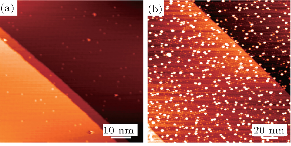 | Fig. 7. Low coverage (a) and high coverage (b) of the silicon clusters located monodispersedly on graphene at room temperature. |
It is worth noting that two small domains in Fig. 8(b) have different orientations (regions A and B). The angle between these two orientations is about 13.2° . For clarity, a sketch map of the diffraction spots of the superstructure in reciprocal space is shown in Fig. 8(c). Aside from the (1× 1) diffraction spots of the Ir (111) lattice, two symmetrical equivalent domains exist (red and blue spots). The schematic diagram of the diffraction spots in real space (Fig. 8(d)) demonstrates that this silicon-induced superstructure is a 
The arrangement of the graphene (G) adlayer and the underneath silicon layer can be further expounded by analyzing the STM images. Figure 9(a) shows the domain boundary between a G/Ir area (with a periodicity of 2.5 nm) in the lower-right part and a G/Si/Ir area (periodicity 1.2 nm) in the upper-left part. It is easy to see several key features in the intercalated area: graphene honeycomb lattice, 

 | Fig. 8. LEED pattern, STM image and the corresponding schematic diagrams of graphene on Ir (111) after silicon intercalation. (a) A group of new spots appearing within the circle of Ir (111) diffraction spots, which is obtained at 67 eV. (b) STM image (U = − 0.38 V, I = 0.13 nA) showing two distinct ordered domains (marked as A and B) with a periodicity of 1.2 nm. (c) Sketch of the diffraction spots shown in panel (a), where the reciprocal vectors of each group of spots are indicated by white, red, and blue arrows respectively. (d) Schematic diagram of the diffraction spots in real space, revealing a  |
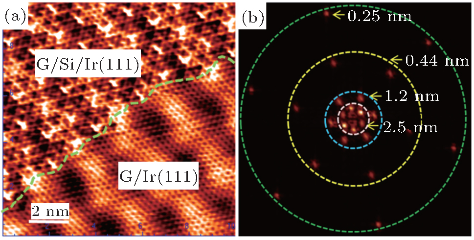 | Fig. 9. Close-up STM image and corresponding FFT pattern at the domain boundary. (a) Atomically resolved image (10 nm × 10 nm, U = − 0.05 V, and I = 0.6 nA) of graphene on Ir (111) with silicon layer underneath on the upper-left region. (b) FFT pattern with four groups of spots with hexagonal symmetry, which reveal four superstructures with different periodicities of 2.5 nm, 1.2 nm, 0.44 nm, and 0.25 nm from inner to outmost circles.[74] |
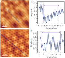
Upon removing intentionally the third large circle of spots from the FFT pattern by a high-pass treatment (see Fig. 10(b)), it will accordingly produce an image that nicely reveals the honeycomb lattice of the topmost layer (Fig. 10(a)). No sign of defects appears in this topmost lattice. It indicates that the graphene lattice on Ir substrate after silicon intercalation is still continuous and intact. Besides the graphene layer, it is % also very important to understand the ordered silicon layer beneath graphene. As discussed above, the spots in the third large circle of the FFT pattern in Fig. 9(b), indicate an ordered superstructure of the silicon layer. In order to obtain a clearer picture of this silicon structure, the information of the topmost graphene honeycomb (0.25 nm in periodicity) is eliminated intentionally from the FFT pattern, as depicted in Fig. 10(d). The corresponding STM image in Fig. 10(c) reveals another honeycomb structure, in the upper-left part of the image, which can be attributed to the underlying silicon layer.
In order to obtain clearer pictures for comparison, the local areas of graphene and silicon lattices in Figs. 10(a) and 10(c) are zoomed in, which are shown in Figs. 11(a) and 11(c), respectively. Figure 11(b) shows the line profile along the blue line in Fig. 11(a), revealing that the periodicity of graphene lattice is about 0.25 nm. For silicon layer, the line profile (along the blue line in Fig. 11(c)) shown in Fig. 11(d) reveals that the periodicity of the silicon honeycombs is about 0.44 nm. That means that the Si– Si distance is about 0.254 nm without considering undulation 
 | Fig. 10. The STM images ((a) and (c)) by intentionally omitting the information of the superstructure presented in Fig. 8 with a periodicity of 0.44 nm and 0.25 nm ((b) and (d)), respectively. These images indicate that the topmost graphene layer (2.5-nm lattice) is intact and continuous (a), and the underlying silicon layer has a honeycomb structure in the upper-left region (c).[74] |
 | Fig. 11. STM image after omitting the information of the superstructure with a periodicity of (a) 0.44 nm and (c) 0.25 nm. (b) Line profile along the blue line in panel (a), revealing the periodicity of graphene after silicon intercalation (0.25 nm). (d) Line profile along the blue line in panel (c), revealing the periodicity of the silicon honeycombs underneath graphene (0.44 nm). |
 | Fig. 12. Perspective view of a schematic diagram, showing silicene– graphene layered superstructures (grey balls indicate carbon atoms and green balls refer to silicon atoms). |
One other thing to note is that compared with silicene on Ir (111) showing a 

In this paper, we review the geometric and electronic properties of silicene and silicene– graphene layered structures on Ir (111) substrate. Silicene sheet can be epitaxially grown on the Ir (111) and it matches with a 

| 1 |
|
| 2 |
|
| 3 |
|
| 4 |
|
| 5 |
|
| 6 |
|
| 7 |
|
| 8 |
|
| 9 |
|
| 10 |
|
| 11 |
|
| 12 |
|
| 13 |
|
| 14 |
|
| 15 |
|
| 16 |
|
| 17 |
|
| 18 |
|
| 19 |
|
| 20 |
|
| 21 |
|
| 22 |
|
| 23 |
|
| 24 |
|
| 25 |
|
| 26 |
|
| 27 |
|
| 28 |
|
| 29 |
|
| 30 |
|
| 31 |
|
| 32 |
|
| 33 |
|
| 34 |
|
| 35 |
|
| 36 |
|
| 37 |
|
| 38 |
|
| 39 |
|
| 40 |
|
| 41 |
|
| 42 |
|
| 43 |
|
| 44 |
|
| 45 |
|
| 46 |
|
| 47 |
|
| 48 |
|
| 49 |
|
| 50 |
|
| 51 |
|
| 52 |
|
| 53 |
|
| 54 |
|
| 55 |
|
| 56 |
|
| 57 |
|
| 58 |
|
| 59 |
|
| 60 |
|
| 61 |
|
| 62 |
|
| 63 |
|
| 64 |
|
| 65 |
|
| 66 |
|
| 67 |
|
| 68 |
|
| 69 |
|
| 70 |
|
| 71 |
|
| 72 |
|
| 73 |
|
| 74 |
|
| 75 |
|
| 76 |
|
| 77 |
|
| 78 |
|
| 79 |
|
| 80 |
|
| 81 |
|
| 82 |
|
| 83 |
|
| 84 |
|
| 85 |
|
| 86 |
|
| 87 |
|
| 88 |
|
| 89 |
|
| 90 |
|