Fabrication and properties of silicene and silicene–graphene layered structures on Ir (111)

Fabrication and properties of silicene and silicene–graphene layered structures on Ir (111) |
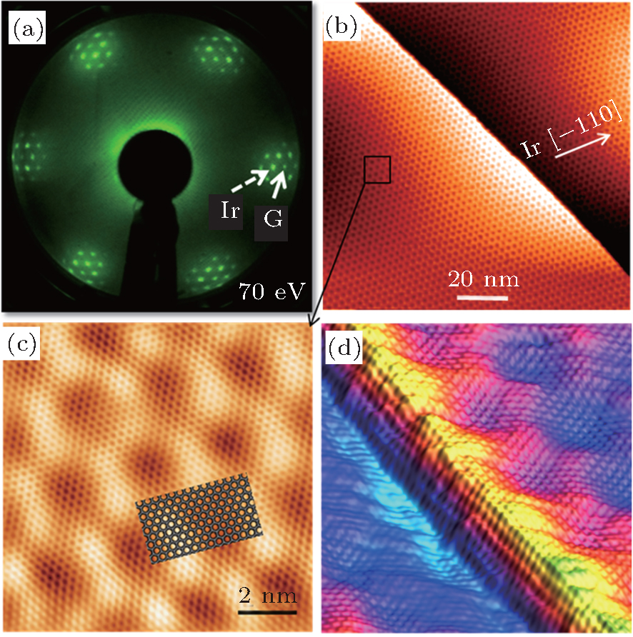
| LEED patterns and STM images of graphene on Ir (111). (a) The inner six spots and the outer six spots, indicated by the dashed-line and solid-line arrows, which are from Ir (111) and the graphene adlayer, respectively, and appear at 70 eV. (b) Large-scale image ( U = −1.54 V, I = 0.05 nA) showing a well-ordered graphene adlayer with a moiré superstructure of 2.5 nm. (c) A zoomed-in image with atomic resolution, and a model that is superimposed on graphene indicating its orientation. (d) 3D STM image of graphene, showing its continuity both on the terrace and at the step edges.[ 74 ] |
 |