Fabrication and properties of silicene and silicene–graphene layered structures on Ir (111)

Fabrication and properties of silicene and silicene–graphene layered structures on Ir (111) |
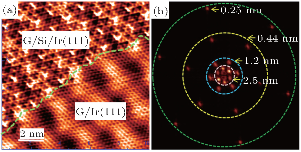
| Close-up STM image and corresponding FFT pattern at the domain boundary. (a) Atomically resolved image (10 nm × 10 nm, U = −0.05 V, and I = 0.6 nA) of graphene on Ir (111) with silicon layer underneath on the upper-left region. (b) FFT pattern with four groups of spots with hexagonal symmetry, which reveal four superstructures with different periodicities of 2.5 nm, 1.2 nm, 0.44 nm, and 0.25 nm from inner to outmost circles.[ 74 ] |
 |