Yu Lei, Zhang Yuan-Wen, Li Kai, Pi Hui, Diao Jia-Sheng, Wang Xing-Fu, Hu Wen-Xiao, Zhang Chong-Zhen, Song Wei-Dong, Shen Yue, Li Shu-Ti†. Theoretical analysis of semi/non-polar InGaN/GaN light-emitting diodes grown on silicon substrates. Chinese Physics B, 24(7): 077801
Permissions
Theoretical analysis of semi/non-polar InGaN/GaN light-emitting diodes grown on silicon substrates
Yu Leia), Zhang Yuan-Wena), Li Kaia), Pi Huia), Diao Jia-Shenga), Wang Xing-Fua), Hu Wen-Xiaoa), Zhang Chong-Zhena), Song Wei-Donga), Shen Yuea), Li Shu-Ti†a),b)
Institute of Opto-electronic Materials and Technology, South China Normal University, Guangzhou 510631, China
Guangdong Engineering Research Center of Optoelectronic Functional Materials and Devices, Guangzhou 510631, China
*Project supported by the National Natural Science Foundation of China (Grant No. 51172079), the Science and Technology Program of Guangdong Province, China (Grant Nos. 2010B090400456 and 2010A081002002), the Science and Technology Program of Guangzhou, China (Grant No. 2011J4300018), and the Program for Changjiang Scholars and Innovative Research Team in Universities of China (Grant No. IRT13064).
Abstract
A theoretical study of polar and semi/non-polar InGaN/GaN light-emitting diodes (LEDs) with different internal surface polarization charges, which can be grown on Si substrates, is conducted by using APSYS software. In comparison with polar structure LEDs, the semi-polar structure exhibits a higher concentration of electrons and holes and radiative recombination rate, and its reduced built-in polarization field weakens the extent of band bending which causes the shift of peak emission wavelength. So the efficiency droop of semi-polar InGaN/GaN LEDs declines obviously and the optical power is significantly improved. In comparison with non-polar structure LEDs, although the concentration of holes and electrons as well as the radiative recombination rate of the semi-polar structure are better in the last two quantum wells (QWs) approaching the p-GaN side, the uniformity of distribution of carriers and radiative recombination rate for the non-polar structure is better. So the theoretical analysis indicates that the removal of the internal polarization field in the MQWs active regions for non-polar structure LEDs contributes to the uniform distribution of electrons and holes, and decreases the electron leakage. Thus it enhances the radiative recombination rate, and further improves the IQEs and optical powers, and shows the best photoelectric properties among these three structures.
PACS:
78.20.Bh; 73.40.Kp; 85.60.Jb; 87.16.ad
Keyword:
semi/non-polar; InGaN/GaN LEDs; APSYS; Si substrate
Gallium nitride (GaN) based light-emitting diodes (LEDs) have been studied for a long time. They are produced along c-plane GaN, which is a highly polar crystal orientation.[1, 2] Along the polar crystal orientation, the piezoelectric and spontaneous polarization induces internal electric fields generated in GaN or between different III-nitride alloys, leading to an efficiency droop of GaN-based LEDs.[3, 4] Therefore, III-nitride alloys grown along a non-polar or semi-polar crystal orientation are attracting extensive attention to eliminate or significantly reduce this effect.[5– 8] In this stage, there are many research groups around the world focusing on experimental research of non-polar or semi-polar III-nitride compound grown on Si substrate. Ravash et al. successfully obtained smooth semi-polar InGaN/GaN MQW structures grown on planar Si(112) substrate by using metal organic chemical vapor deposition (MOCVD).[9] Due to the large lattice mismatch and the thermal expansion mismatch, different approaches of strain engineering have been adopted in order to achieve non-polar or semi-polar crack-free GaN layers, and the sophisticated method is the growth of III-nitride compound on pre-patterned Si substrates.[10] In the existing literature, non-polar GaN films grown on pattern Si(112) substrates are reported, [11] and the commonly favored crystal orientation of Si substrates on which semi-polar GaN films can grow is (100) orientation facet. The semi-polar GaN grown by selective lateral overgrowth can coalesce to form planar GaN films with low dislocation density and reasonable crystal quality, [12] and advances have been achieved by the use of 7° -off (001) Si substrates with V-grooves.[13, 14] High-performance semi-polar or non-polar GaN-based LED devices are promising for being produced on the basis of this method.[15]
The reports about semi-polar or non-polar GaN grown on Si substrates discussed above were all experimental studies. Furthermore, they expounded the growth, characterization, and optical properties of semi-polar or non-polar GaN grown on Si substrates. Except in experimental studies, theoretical analysis of the polarization characteristics of III-nitride compound has been seldom reported, especially theoretical analysis of a comparison between semi/non-polar and polar InGaN/GaN LEDs grown on Si substrates. The reduction of internal polarization field in semi-polar (1-101) InGaN/GaN LEDs leads to uniform distribution of carriers and reduces the electron leakage according to the simulated results in Ref. [16]. However, their research has not mentioned non-polar GaN-based LEDs. Andreev et al. simulated a-plane (non-polar), semi-polar, and c-plane (polar) InGaN MQWs LEDs with high In contents by using an in-house developed software called CELS/Quatra, [17] but the analysis of simulation results was relatively limited, without discussing built-in polarization field and distribution of carriers.
In this paper, we present the improvement between polar and semi/non-polar InGaN-based LEDs in detail. The results are simulated by the advanced physical models of semiconductor devices (APSYS) software, which is used frequently and approved by many researchers in the field of LED device simulation. A lot of references indicated that the simulation results of GaN-based LED devices by using the APSYS software are similar to the experimental results and it is instructive and meaningful to the experimental research of GaN-based LEDs.[16, 18] We mainly aim at the analysis of the superiority of LED internal efficiency, total power, carriers concentrations, radiative recombination rate, blue shift of wavelength, etc. in the InGaN/GaN MQW LEDs with different internal polarization. The improvement of non-polar and semi-polar structures on the performance of LEDs in this paper is in accordance with the literature.[16, 17, 19] The results of efficiency droop, carrier distribution, and energy diagram comparing non-polar structure with conventional polar structure are similar to the experiment results in Ref. [19], and the comparison between semi-polar structure and conventional polar structure also exhibits the similar improvement with the experiment analysis in Ref. [16].
2. Structure and parameters
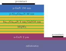
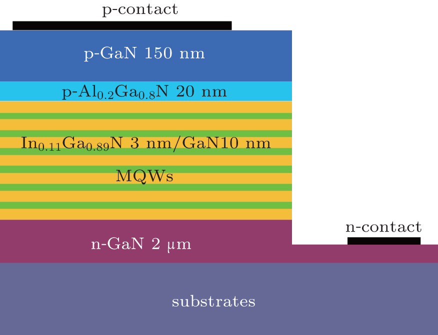
In the LED device structure shown in Fig. 1, the conventional blue InGaN/GaN MQWs LED is used as the reference structure to be simulated in this paper.[20] The device structure mainly consists of a 2-μ m-thick n-type GaN:Si (5× 1018 cm− 3) layer, six periods of In0.11Ga0.89N(3 nm)/GaN(10 nm) MQWs active regions, followed by a 20-nm-thick p-type Al0.2Ga0.8N:Mg (3× 1017 cm− 3) electron blocking layer (EBL), and a 0.15-μ m-thick p-type GaN:Mg (1.2× 1018 cm− 3) cap layer. The n-type doping concentration of the GaN barrier layer is 3× 1017 cm− 3. The device geometry is 300× 300 μ m2.
Fig. 1. Schematic of InGaN/GaN-based LED structure.
In this paper, we set three structures: structure A acts as a polar InGaN/GaN LED, structure B acts as a semi-polar InGaN/GaN LED, and structure C acts as a non-polar InGaN/GaN LED. In the process of simulation, the theoretical built-in interface polarization charge values are calculated according to the method developed by Fiorentini et al., [21, 22] and in their opinions the polarization interface charge densities in the simulation of InGaN-based LEDs are assumed to be mainly dependent on the composition and strain in III– V nitride wurtzite alloys. In the process of simulation, we assume that these three samples with different polarities possess the same crystal quality and the influence of stress condition is similar in these three structures LEDs, since the GaN grown on substrates can be considered as approximate relaxation after the thickness of GaN grown on substrates exceeds 2 μ m[23, 24] and the stress mainly comes from the lattice mismatch between InGaN/GaN MQWs and AlGaN EBL. In addition, we assume that the Coulomb screening effect is also similar among these three structures LEDs. Because the quantity of electrons and holes induced by the applied voltage of different polarities structures LEDs is similar under the same injection current density. In this paper, we only set built-in interface polarization charge densities by changing the percentage of the theoretical interface polarization charge densities calculated by Fiorentini et al. The interface charge densities of polar structure A are assumed to be 50% of the theoretical values, [2] semi-polar structure B with 30% , and non-polar structure C with no interface charge densities. Other parameters of the device structures are the same. The band-offset radio of both InGaN and AlGaN materials is set to be 0.7/0.3, the internal loss within the LED device is assumed to be 2000 m− 1 and the operating temperature is assumed to be 300 K. Other detailed material parameters of the semiconductors used in this simulation can be found in Ref. [25] or are in accordance with the defaults of the software.
3. Results and discussion
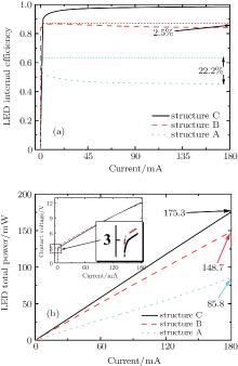
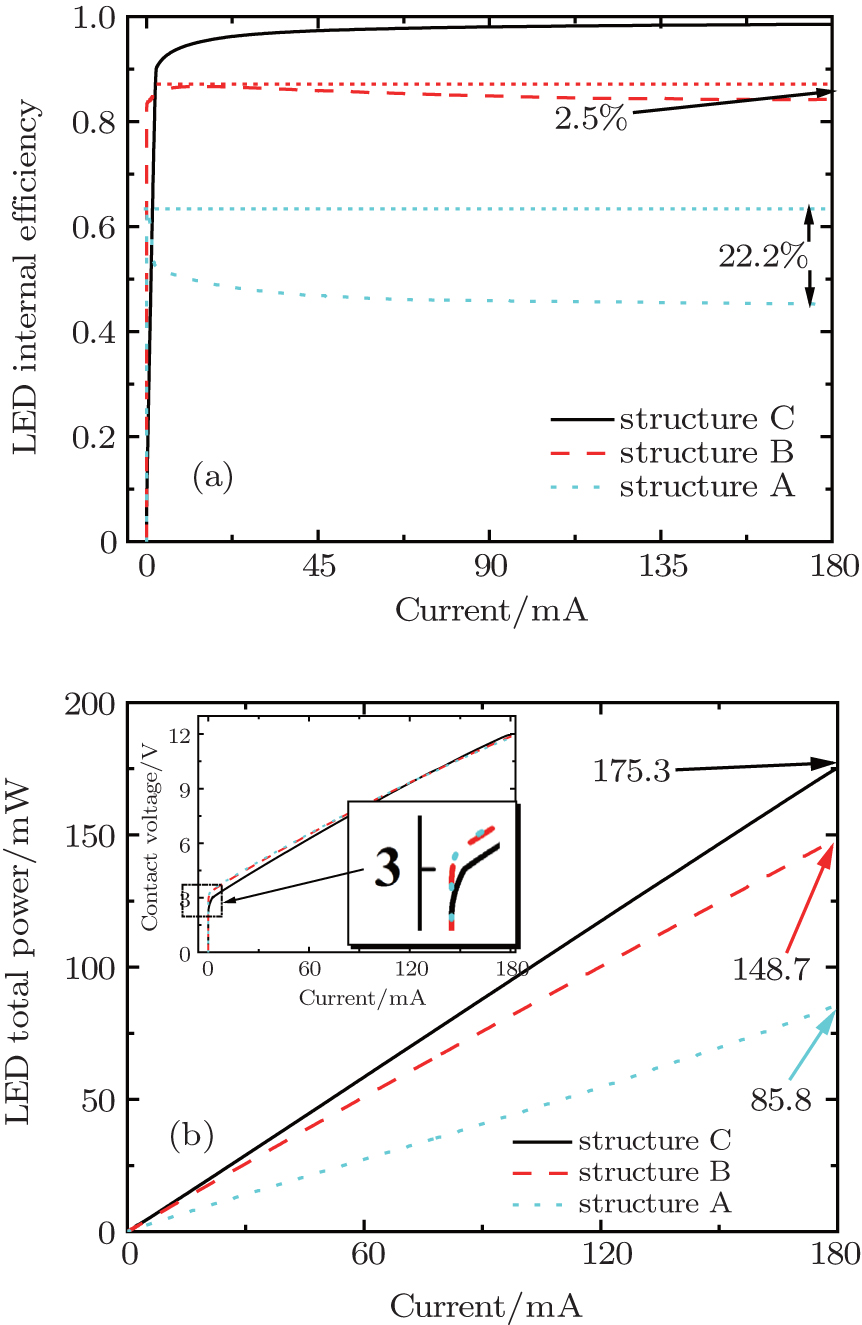
Regarding the effect of reducing the internal surface polarization on the performances of InGaN/GaN-based LEDs, we firstly demonstrate the optical powers and IQEs of the three structures as illustrated above. In Fig. 2(a), the internal efficiency of the non/semi-polar InGaN/GaN LED is obviously higher than the polar InGaN/GaN LED, and the IQE of the non-polar structure C is the best, since the value has already reached 98.6% , without efficiency droop, as the injection current increases. However, the efficiency droop of polar structure A is severe compared with the other two structures. The maximum efficiency droop arrives at 22.2% while it decreases to 2.5% in semi-polar structure B under high injection current. The high build-in internal electric field generated by spontaneous polarization and piezoelectric polarization in the polar structure A LED device induces the spatial separation of the electron and hole wave function, then reduces the effective radiative recombination rate of electrons and holes in active regions. Moreover, plenty of electrons are injected into MQW regions under high injection current, and severe band bending aggravates the electron overflow shown in Fig. 3(a), [26] which can also lead to a larger efficiency droop. Hence, a large efficiency droop is observed in polar structure A shown in Fig. 2(a). In Fig. 2(b), the optical powers of the three structures are all enlarged by the increasing of the injection current. The higher optical power appears in the structure with lower internal polarization charges. At a 180 mA contact current, the total powers of structures A, B, and C are 85.8 mW, 148.7 mW, and 175.3 mW, respectively. From these values, it can be clearly seen that the output power of the non-polar structure’ s LED is more than twice that of the polar. This improvement is further confirmed by the C– V diagram in the inset of Fig. 2(b). The depressed turn-on voltage can be seen from the inset for non-polar structure C because of its few internal polarization charges. However, the turn-on voltage of structures A and B are almost the same, because the built-in polarization is not completely cleared away and results in energy band bending (see Fig. 3).
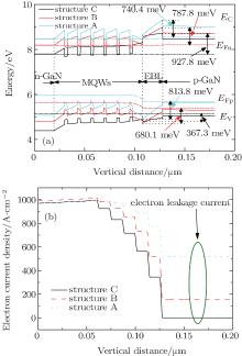
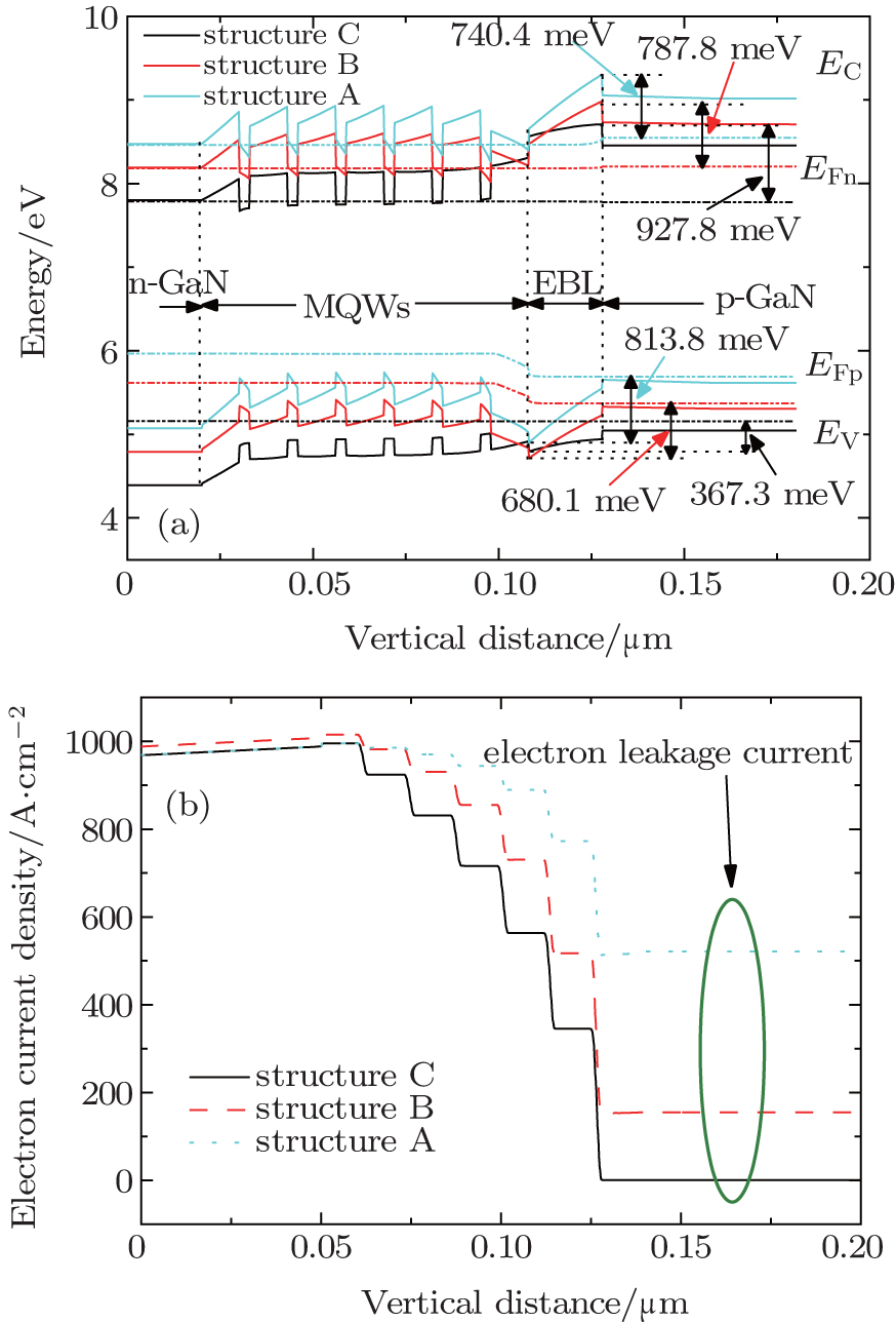
Fig. 3. The energy band diagrams (a) and electron leakage current (b) at 180 mA injection current for polar (A), semi-polar (B), and non-polar (C) structure InGaN/GaN LEDs.
Figure 3(a) shows the energy band diagrams and quasi-Fermi levels of the three structures at an injection current of 180 mA. Considering that relevant references all adopted the same band gaps in studying the influence of the effect of polarity on the performances of the GaN-based LEDs.[16, 17, 19, 27] Therefore, we simply use the same band gaps for the three structures LEDs along three different crystal orientations in this paper. In Fig. 3(a), we can observe a severe situation of band bending, sloped triangular barriers and wells for polar and semi-polar structures. Furthermore, the conduction band bends upward while it approaches the MQWs active regions of the n-GaN side, and the conduction band close to the p-GaN side of the MQWs active regions is obviously lower than the n-GaN side.[19] As a result, the effective potential barrier height of the conduction band in the EBL for structures A and B reduces significantly compared with non-polar structure C, falling to 787.8 meV for semi-polar structure B and falling to 740.4 meV for polar structure A. Therefore, if we observe the large electron leakage current in Fig. 3(b), polar structure A is higher than the semi-polar structure B because of its worse band bending and lower potential barrier height. In addition, the conduction band of the n-side is higher than theconduction band of the p-side for all QWs, which results in the electrons gathering in the p-side of active regions. As a result, a high carrier concentration can be observed in the last several QWs approaching the p-GaN side (see Fig. 4), leading to the severe non-uniform distribution of electrons and holes in MQWs regions, especially for structures A and B. It reveals that the large electron leakage current caused by the built-in polarization field is the main mechanism resulting in a dramatic efficiency droop. For non-polar structure C, its GaN QBs do not exhibit obvious band bending and triangular shape energy band. Moreover, the potential barrier height of the conduction band in EBL, reaching 927.8 meV, is higher than those of structures A and B. Consequently, only a tiny electron leakage current, close to zero, appears in Fig. 3(b).
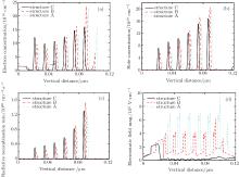
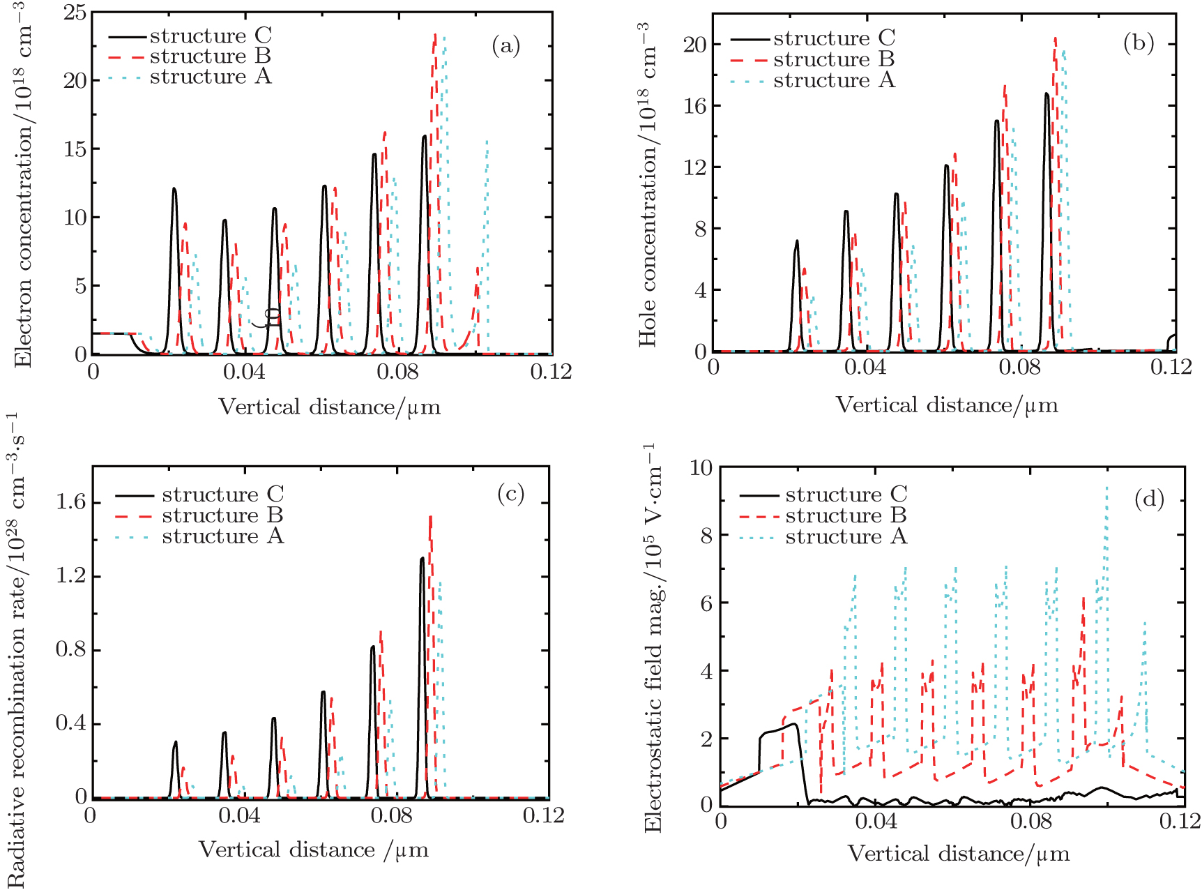
Fig. 4. The distribution of electron concentration (a), hole concentration (b), radiative recombination rate (c), and polarization electrostatic field (d) of InGaN/GaN MQWs at 180 mA injection current for polar (A), semi-polar (B), and non-polar (C) structure InGaN/GaN LEDs.
Compared with Ref. [17], we analyze the carrier distribution and carrier radiative recombination rate (RRR) distribution in detail. In Fig. 4, note that the horizontal position of the vertical distance in the LED layer has been shifted slightly for better observation. It is obvious that the distribution of the carrier concentration for non-polar structure C exhibits optimum uniformity, though it performs a similar distribution trend that the QWs approaching the p-GaN side have higher carrier concentration than the QWs approaching the n-GaN side, resulting from the relatively larger effective mass and the lower mobility for holes and the reverse situation for electrons. The p-AlGaN EBL also plays a vital role in gathering carriers in MQWs regions, as shown in Fig. 3(a). The distinct non-uniform distribution of carriers in structures A and B is due to the higher internal interface polarization electrostatic field of MQW active regions, as shown in Fig. 4(d). In Figs. 4(a) and 4(b), it can be observed that the concentrations of electrons and holes for structures B and C are all higher than that of polar structure A, resulting from the increase in effective potential barrier height in the conduction band and decrease of effective potential barrier height in the valence band. A comparison of structures B and C indicates that the higher barrier height, reaching 927.8 meV, in the conduction band suppresses the electrons overflowing to the p-side, and the lower barrier height, reaching 367.3 meV, in the valence band promotes the holes flowing into MQWs active regions for non-polar structure C. This results in the uniform distribution of carriers in MQW active regions. Hence, the relative uniform RRR of electrons and holes for non-polar structure C can be observed in Fig. 4(c).
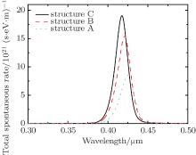
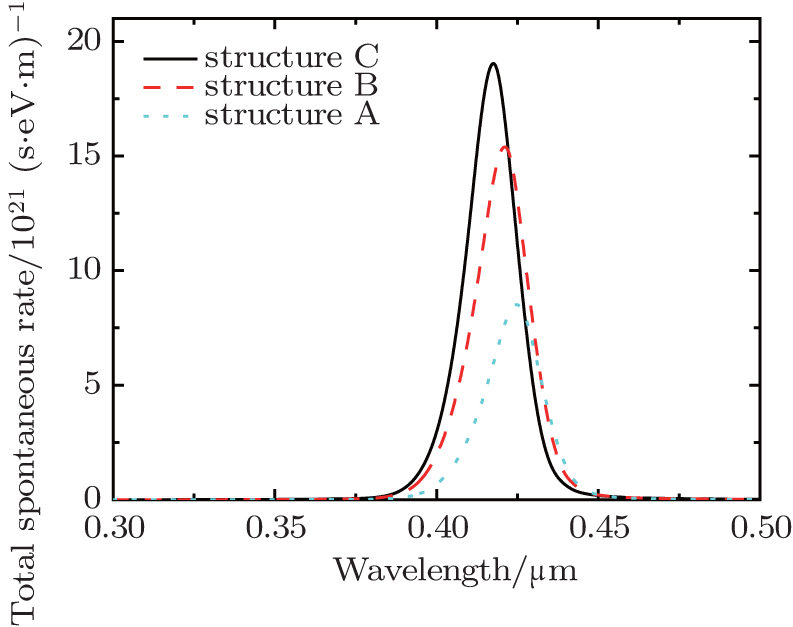
Figure 5 shows the total spontaneous emission rate of InGaN/GaN MQWs at a 137 mA injection current for these three structures. We can observe that the peak wavelength blue shifts obviously with the decrease in the internal polarization charge densities for structures A, B, and C. The blue shift arises from the quantum confined stark effect (QCSE), resulting from built-in polarization field.[17] The QCSE leads to band bending, restricting the carrier radiative recombination efficiency, enlarging the emission wavelength of high internal polarization charges GaN-based LEDs. Considering the reduced effective energy gap resulting from band bending in the structures with high built-in polarization field shown in Figs. 3(a) and 4(d), we conclude that the higher the polarization field of a structure, the severer the band bending for this structure. Thus, the shortest wavelength appears in the non-polar structure C because of its widest effective energy gap, resulting from the lowest built-in polarization field, among these three structures. Here, we can also observe that the intensity of the peak wavelength of non-polar structure C is the highest, in accordance with its superior performances of its highest IQEs and optical power, among these three structures.
Fig. 5. The total spontaneous emission rate of MQWs at 137 mA injection current for polar (A), semi-polar (B), and non-polar (C) InGaN/GaN LEDs.
4. Conclusions
In summary, the photoelectric properties of polar, semi-polar, and non-polar InGaN/GaN-based LEDs grown on Si substrates are studied in detail. For the non-polar structure, the internal quantum efficiency (IQE) arriving at 98.6% and optical power are much higher than those of the semi-polar and polar structures. The slightest energy band bending also occurs in the non-polar structure with the least turn-on voltage, and the minimum built-in polarization field and electron leakage current are exhibited in the non-polar structure among the three structures. Although the concentrations of holes and electrons as well as the radiative recombination rate of semi-polar structure are better in the last two quantum wells (QWs) approaching the p-GaN side, the uniformity of distribution of carriers and radiative recombination rate for the non-polar structure is better, compared with the semi-polar structure. Our analysis indicates that the efficiency droop and photoelectric properties of non-polar structure LEDs exhibit optimal improvement, the semi-polar structure LEDs also show enhanced performances in comparison with the polar structure LEDs. These conclusions, including the optical and electrical performances of the non-polar or semi-polar InGaN/GaN-based LEDs in this paper, can be used as a theoretical foundation for following experimental research of the high-performance semi/non-polar InGaN/GaN-based LEDs grown on Si substrates.
... [1,2] Along the polar crystal orientation, the piezoelectric and spontaneous polarization induces internal electric fields generated in GaN or between different III-nitride alloys, leading to an efficiency droop of GaN-based LEDs ...
2
2014
0.0
0.0
... [1,2] Along the polar crystal orientation, the piezoelectric and spontaneous polarization induces internal electric fields generated in GaN or between different III-nitride alloys, leading to an efficiency droop of GaN-based LEDs ...
... of the theoretical values,[2] semi-polar structure B with 30#cod#x00025 ...
1
1997
0.0
0.0
... [3,4] Therefore, III-nitride alloys grown along a non-polar or semi-polar crystal orientation are attracting extensive attention to eliminate or significantly reduce this effect ...
1
2000
0.0
0.0
... [3,4] Therefore, III-nitride alloys grown along a non-polar or semi-polar crystal orientation are attracting extensive attention to eliminate or significantly reduce this effect ...
1
2006
0.0
0.0
... [5#cod#x2013 ...
1
2012
0.0
0.0
1
2012
0.0
0.0
1
2010
0.0
0.0
... 8] In this stage, there are many research groups around the world focusing on experimental research of non-polar or semi-polar III-nitride compound grown on Si substrate ...
1
2013
0.0
0.0
... [9] Due to the large lattice mismatch and the thermal expansion mismatch, different approaches of strain engineering have been adopted in order to achieve non-polar or semi-polar crack-free GaN layers, and the sophisticated method is the growth of III-nitride compound on pre-patterned Si substrates ...
1
2014
0.0
0.0
... [10] In the existing literature, non-polar GaN films grown on pattern Si(112) substrates are reported,[11] and the commonly favored crystal orientation of Si substrates on which semi-polar GaN films can grow is (100) orientation facet ...
1
2011
0.0
0.0
... [10] In the existing literature, non-polar GaN films grown on pattern Si(112) substrates are reported,[11] and the commonly favored crystal orientation of Si substrates on which semi-polar GaN films can grow is (100) orientation facet ...
1
2010
0.0
0.0
... The semi-polar GaN grown by selective lateral overgrowth can coalesce to form planar GaN films with low dislocation density and reasonable crystal quality,[12] and advances have been achieved by the use of 7#cod#x000B0 ...
1
2013
0.0
0.0
... [13,14] High-performance semi-polar or non-polar GaN-based LED devices are promising for being produced on the basis of this method ...
1
2013
0.0
0.0
... [13,14] High-performance semi-polar or non-polar GaN-based LED devices are promising for being produced on the basis of this method ...
1
2008
0.0
0.0
... [15] ...
5
2011
0.0
0.0
... [16] ...
... [16,18] We mainly aim at the analysis of the superiority of LED internal efficiency, total power, carriers concentrations, radiative recombination rate, blue shift of wavelength, etc ...
... [16,17,19] The results of efficiency droop, carrier distribution, and energy diagram comparing non-polar structure with conventional polar structure are similar to the experiment results in Ref ...
... [16] ...
... [16,17,19,27] Therefore, we simply use the same band gaps for the three structures LEDs along three different crystal orientations in this paper ...
5
2012
0.0
0.0
... simulated a-plane (non-polar), semi-polar, and c-plane (polar) InGaN MQWs LEDs with high In contents by using an in-house developed software called CELS/Quatra,[17] but the analysis of simulation results was relatively limited, without discussing built-in polarization field and distribution of carriers ...
... [16,17,19] The results of efficiency droop, carrier distribution, and energy diagram comparing non-polar structure with conventional polar structure are similar to the experiment results in Ref ...
... [16,17,19,27] Therefore, we simply use the same band gaps for the three structures LEDs along three different crystal orientations in this paper ...
... [17], we analyze the carrier distribution and carrier radiative recombination rate (RRR) distribution in detail ...
... [17] The QCSE leads to band bending, restricting the carrier radiative recombination efficiency, enlarging the emission wavelength of high internal polarization charges GaN-based LEDs ...
1
2011
0.0
0.0
... [16,18] We mainly aim at the analysis of the superiority of LED internal efficiency, total power, carriers concentrations, radiative recombination rate, blue shift of wavelength, etc ...
4
2010
0.0
0.0
... [16,17,19] The results of efficiency droop, carrier distribution, and energy diagram comparing non-polar structure with conventional polar structure are similar to the experiment results in Ref ...
... [19], and the comparison between semi-polar structure and conventional polar structure also exhibits the similar improvement with the experiment analysis in Ref ...
... [16,17,19,27] Therefore, we simply use the same band gaps for the three structures LEDs along three different crystal orientations in this paper ...
... [19] As a result, the effective potential barrier height of the conduction band in the EBL for structures A and B reduces significantly compared with non-polar structure C, falling to 787 ...
1
2013
0.0
0.0
... [20] The device structure mainly consists of a 2-#cod#x003BC ...
1
2002
0.0
0.0
... ,[21,22] and in their opinions the polarization interface charge densities in the simulation of InGaN-based LEDs are assumed to be mainly dependent on the composition and strain in III#cod#x02013 ...
1
2001
0.0
0.0
... ,[21,22] and in their opinions the polarization interface charge densities in the simulation of InGaN-based LEDs are assumed to be mainly dependent on the composition and strain in III#cod#x02013 ...
1
2005
0.0
0.0
... m[23,24] and the stress mainly comes from the lattice mismatch between InGaN/GaN MQWs and AlGaN EBL ...
1
2001
0.0
0.0
... m[23,24] and the stress mainly comes from the lattice mismatch between InGaN/GaN MQWs and AlGaN EBL ...
1
2001
0.0
0.0
... [25] or are in accordance with the defaults of the software ...
1
2011
0.0
0.0
... 3(a),[26] which can also lead to a larger efficiency droop ...
1
2013
0.0
0.0
... [16,17,19,27] Therefore, we simply use the same band gaps for the three structures LEDs along three different crystal orientations in this paper ...
Theoretical analysis of semi/non-polar InGaN/GaN light-emitting diodes grown on silicon substrates
[Yu Leia), Zhang Yuan-Wena), Li Kaia), Pi Huia), Diao Jia-Shenga), Wang Xing-Fua), Hu Wen-Xiaoa), Zhang Chong-Zhena), Song Wei-Donga), Shen Yuea), Li Shu-Ti†a),b)]


 ]
]