†Corresponding author. E-mail: zhbaij@mail.sysu.edu.cn
*Project supported by the National Natural Science Foundation of China (Grant Nos. 61274039 and 51177175), the National Basic Research Program of China (Grant Nos. 2010CB923201 and 2011CB301903), the Ph. D. Program Foundation of the Ministry of Education of China (Grant No. 20110171110021), the International Science and Technology Collaboration Program of China (Grant No. 2012DFG52260), the National High Technology Research and Development Program of China (Grant No. 2014AA032606), the International Science and Technology Collaboration Program of Guangdong Province, China (Grant No. 2013B051000041), and the Opened Fund of the State Key Laboratory on Integrated Optoelectronics (Grant No. IOSKL2014KF17).
The influences of stress on the properties of InGaN/GaN multiple quantum wells (MQWs) grown on silicon substrate were investigated. The different stresses were induced by growing InGaN and AlGaN insertion layers (IL) respectively before the growth of MQWs in metal–organic chemical vapor deposition (MOCVD) system. High resolution x-ray diffraction (HRXRD) and photoluminescence (PL) measurements demonstrated that the InGaN IL introduced an additional tensile stress in n-GaN, which released the strain in MQWs. It is helpful to increase the indium incorporation in MQWs. In comparison with MQWs without the IL, the wavelength shows a red-shift. AlGaN IL introduced a compressive stress to compensate the tensile stress, which reduces the indium composition in MQWs. PL measurement shows a blue-shift of wavelength. The two kinds of ILs were adopted to InGaN/GaN MQWs LED structures. The same wavelength shifts were also observed in the electroluminescence (EL) measurements of the LEDs. Improved indium homogeneity with InGaN IL, and phase separation with AlGaN IL were observed in the light images of the LEDs.
GaN/InGaN blue LEDs have been widely used in commerce because of their many advantages such as energy conservation, high efficiency, safety, and long durability. Recently, GaN-based green/yellow LEDs have been given more attention due to their bright and broad application prospects. However, some difficulties still remain in growing high quality, high-indium InGaN multiple quantum wells (MQWs), because of the large stresses, high threading dislocation density in MQWs, low indium incorporation efficiency, and so on. Strain-induced piezoelectric polarization and spontaneous polarization[1, 2] bring in large internal electrostatic fields, [3] which causes the separation of electron and hole wave function, [4, 5] resulting in low internal quantum efficiency. Meanwhile, due to the low cost and large scale, Si substrates have been extensively studied for the growth of GaN-based materials, but LEDs on Si substrates simultaneously face more challenges.[6, 7] One difficulty is the stress control on the un-doped GaN materials and n-doped GaN prior to the MQWs. InGaN or InGaN/GaN superlattice prestrain layer has been extensively investigated on MQWs/LED on sapphires, [8– 16] and it is reported that there were many functions with these layers such as relieving strain in the upper MQWs and weakening QCSE, [8, 10, 14– 16] improving current spreading, [8, 9] having a more uniform indium composition in the QWs, [13] reducing the density of V-pits in MQWs, [15, 16] and enhancing the internal quantum efficiencies.[8, 16] In all these reports, the wavelength shows a blue-shift[17] in PL and EL measurements, because the tilts of the conduction band and valence band were relieved by weakening the QCSE when the InGaN prestrain layer was utilized. However, in our experiments, an obvious red-shift of wavelength was observed as tensile stress increased, using InGaN IL prior to MQWs active layer. Chen et al. also observed this phenomenon in their experiments; [18] however, they did not analyze the influences of stresses. In the present work, a different IL was grown under the MQWs to change the stress. The influences of stresses on the properties of GaN/InGaN MQWs on Si substrates were investigated.
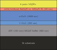
Three kinds of GaN/InGaN MQWs structures with different insertion layers were grown on Si (111) substrates in a Thomas Swan MOCVD system. Trimethylaluminum (TMAl), trimethylindium (TMIn), and ammonia were used as the precursors of aluminum, indium, and nitrogen. The silane and Bis (cyclopentadienyl) magnesium (Cp2Mg) were used as an n-type and p-type doping source respectively. Triethylgallium (TEGa) was used as the gallium precursor for the growth of InGaN layers while trimethylgallium (TMGa) was used for the growth of GaN and AlGaN layers. At first, an Al monolayer was predeposited on Si substrate, after that 100-nm AlN and 660-nm linearly graded AlGaN were grown at 1060 ° C as buffer layers. A 200-nm nominally undoped GaN layer and a 1.0-μ m Si-doped n-GaN (n ∼ 2 × 1018 cm− 3) layer were grown at 1040 ° C, followed by six periods of InGaN/GaN MQWs grown at the temperature of 794 ° C for wells and 916 ° C for barriers. For sample M1, a 20-nm thick In0.1GaN0.9 IL was inserted between n-GaN and MQWs active layers. For sample M3, a 20-nm thick Al0.2Ga0.8N IL was grown on under the MQWs instead of the In0.1GaN0.9 IL. Both InGaN IL and AlGaN IL were doped by silane with carrier concentration around 1 × 1018 cm− 3. For comparison, a control sample without any ILs was also grown in our experiments, and labeled sample M2. Their structure schematic diagrams are shown in Fig. 1.
High-resolution x-ray diffraction (HRXRD) was employed to characterize crystal qualities, indium composition, and thicknesses of MQWs using a Bruker-AXS D8 Discover diffractometer. Reciprocal space mapping (RSM) measurements of GaN (10-15) identified the strain states in MQWs. PL spectra were measured at room temperature with a 325-nm He– Cd laser. The MQWs surface morphologies were carried out by a Veeco Edge atomic force microscope (AFM).
The XRD ω /2θ scans around GaN (0004) of sample M1, M2, and M3 are shown in Fig. 2. The indium composition can be determined by the peak of InGaN QW.[19] With qualitative analysis, sample M1 with InGaN IL shows the smallest degree of InGaN zero-order peak and a small shift of the satellite peaks; the medium one is the sample M2 without any ILs, and sample M3 with AlGaN IL has the largest degree. This implies that the average indium content of InGaN wells in sample M1 is higher than that in sample M2, while in sample M3 the indium content of InGaN wells is the lowest. For acquiring more detailed information about the MQWs’ indium content and structure, simulations are made to fit the experimental XRD data. From this procedure, the average indium composition in the InGaN wells is found to be 15.2%, 14.5%, and 13.2% for sample M1, M2, and M3, respectively. This result is obtained based on the assumption that the epilayer is fully strained, resulting in an underestimation of the indium content value in the case where the epilayer is partially relaxed.[20] Based on the ω /2θ scan curves and simulation, the indium incorporation efficiency in MQWs may be influenced by the stress prior to the MQWs active layer. Compared with sample M2, while the tensile stress prior to the MQWs layer is increased in sample M1, the indium incorporation in wells is effectively improved. Meanwhile, when we introduce compressive stress prior to the MQWs layer in sample M3, the indium incorporation is suppressed.
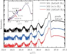 | Fig. 2. XRD (0004) ω /2θ scan measurements of sample M1 (with InGaN IL), sample M2 (without IL), sample M3 (with AlGaN IL), an enlarged view of InGaN zero-order peaks is shown in the inset. |
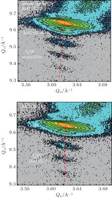
To investigate the mechanism of the influence of stress on the indium incorporation in InGaN wells, reciprocal space mapping (RSM) around the asymmetric (10-15) diffraction was carried out on sample M1 and sample M3, as shown in Fig. 3. The diffraction peaks of MQWs are quite different between samples M1 and M3. For sample M3, the InGaN diffraction peaks are almost in vertical alignment, which demonstrates that InGaN QW layers are nearly coherently strained to the underlying n-GaN layer. However, in the case of sample M1, the diffraction peaks shift somewhat to the left with an inclination, which demonstrates that the QW layers are partially relaxed. A slight shift with diffraction peaks occurs in sample M2, but not so obvious compared with sample M1 (not shown here).
The residual in-plane strain of the n-GaN under MQWs can be figured out using Raman shift as[21]

where Δ Ω is the frequency shift of the E2 phonon mode. While the E2 phonon frequencies of three samples are nearly the same at 568.7± 0.2 cm− 1, the residual strain in the n-GaN layer is -0.091% and the minus denotes compressive strain. By using the data measured from RSM, the biaxial in-plane strains of GaN barriers were calculated to be 0.025%, − 0.030%, and − 0.082% for samples M1, M2, and M3, respectively. This shows that the InGaN IL introduces an additional tensile stress, releasing the strain in the MQWs and AlGaN IL.
It has been reported that there was a compositional pulling effect in the strain InGaN film.[22] Due to the large lattice mismatch, the indium atoms will be excluded from the InGaN film to reduce the deformation energy, resulting in lower indium content in the InGaN film with increasing the thickness of the film. The indium composition finally reaches a constant at a nominal value until beyond the critical thickness. This compositional pulling effect has been found in InGaN film and InGaN/GaN MQWs grown on the GaN or AlGaN templates.[22– 24] For sample M1, the in-plane strain in the MQWs layers was relaxed partially, so the compositional pulling effect in the wells was weakened, and the indium incorporation efficiency increased in the QW. In contrast, sample M3 shows a lower indium composition in the QW due to strengthening of the compositional pulling effect.
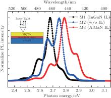
In order to further study the influence of stress on MQWs emitting wavelengths, PL measurements of the three samples were carried out. To exclude the influences of inconsistent wavelengths from center to edge on wafers, we chose the same zone at the center of each wafer in a ϕ 5 mm area. As shown in Fig. 4, the multi-peak of curves in PL spectra is attributed to the Fabry– Perot mode interference between epilayer-Si substrate and epilayer-air interface.[25] The central wavelengths and FWHMs were obtained by Gauss fitting. According to the Gauss fitting of PL spectra, the photon energy of samples M1, M2, and M3 are 2.672 eV, 2.717 eV, and 2.799 eV, respectively. In comparison with sample M2, the photon energy of sample M1 shows a red-shift, while sample M3 shows a blue-shift. The FWHMs of the spectra are 0.122 eV, 0.155 eV, and 0.149 eV for M1, M2, and M3, respectively. The minimum FWHM of M1 with InGaN IL suggests it has the most uniform indium composition distribution. As previously analyzed, the InGaN IL introduces an additional tensile stress on n-GaN, and AlGaN IL introduces a compressive stress to compensate the tensile stress, and the strain in QWs is released as tensile stress increases. In most reports (normally on sapphire) the wavelength is blue-shifted by introducing tensile stress because of weakening the polarization-induce quantum-confined Stark effect (QCSE), but that is not inconsistent with our results. Even though we cannot explain the different wavelength variation tendency between MQWs on Si substrate and sapphire substrate, in our research the increment of indium content that results from weakening the compositional pulling effect may play a dominant role in the wavelength shift of PL on samples grown on Si, resulting in a red-shift of wavelength.
According to Figs. 2 and 3, clear satellite peaks up to the fifth order on the (004)-face ω /2θ scan and third order on the (105) RSM mapping can be observed in the samples, which suggests that there is no significant difference in interface quality among these samples. To further investigate the influence on the surface morphologies properties, 3 μ m× 3 μ m areas of AFM scan were performed, as presented in Fig. 5. The densities of V-pits shown in Fig. 5 are basically equal to each other around 3.75± 0.04× 109 cm− 2. There are still some controversies on the formation mechanism of V-pits.[16, 26, 27] In our results, we support that the density of V-pits is independent of the strain state in MQWs layers, [26] and this is different from the result of Nanhui and co-workers.[16] As the samples are grown on the same structural n-GaN with density of threading dislocations (TDs) around 7.8× 109 cm− 2, which is calculated by XRD (0002) and (10-12) rocking curves, we consider that the densities of V-pits in MQWs are determined by the density of TDs at the underlying templates rather than the strain. The density of V-pits is lower than the density of TD, because not all TDs form V-pits at the end.[28]
All data of the samples are summarized in Table 1. The XRD data were extracted from the rocking curves and (004) ω /2θ scan measurements. PL data were extracted from Gauss fit on samples M1, M2, and M3.
 | Fig. 5. AFM surface morphology of (a) sample M1, (b) sample M2, (c) sample M3, scan size: 3 μ m× 3 μ m; microstructures indicated by arrows are indium-rich clusters formed in V-pits. |
| Table 1. All data of samples M1, M2, and M3. |
Three kinds of LED structures, labeled LED1 (with InGaN IL), LED2 (without IL), and LED3 (with AlGaN IL), were also grown and fabricated by traditional processes. An Ni (5 nm)/Au (7 nm) layer was deposited on the 220-nm p-GaN layer to serve as an Ohmic contact layer, and Cr (20 nm)/Pd (40 nm)/Au (200 nm) were employed as p- and n-type electrodes. The size of the LED chips was 1 mm× 1 mm. Figure 6(a) shows the electroluminescence (EL) spectra of three LEDs at injecting current of 350 mA. In comparison with the LED without IL, the wavelength of the LED with InGaN IL presents an obvious red-shift, and the LED with AlGaN IL presents a blue-shift. According to XRD measurement, we obtain that the indium composition in LED1, LED2, and LED3 is 23.8%, 21.9%, and 19.7%, respectively. This agrees well with previous results. Large surface light images of the LEDs at 50-mA current are shown in Fig. 6(b). The LED2 without IL layer shows an inhomogeneous light image, which is mostly caused by indium compositional fluctuation in the wells. The compositional fluctuation is strengthened as indium composition increases in the wells. However, for the LED1 with InGaN IL, the light image is more uniform than that of LED2, and it presents more spatially homogeneous luminescence. That is attributed to the improvement of in-plane indium composition uniformity in the QWs[13] and better current spreading under the MQWs active region[8, 9] although its indium composition increased. In addition, obvious phase separation can be observed on the surface light image of LED3 with AlGaN IL. A few bright localized dot-like luminescence spots
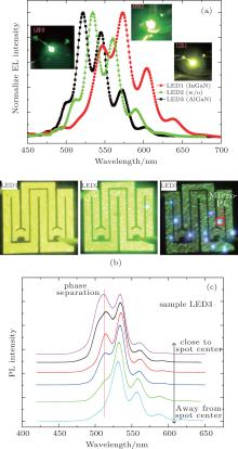 | Fig. 6. (a) EL spectra of LED1 (with InGaN IL), LED2 (without IL), LED3 (with AlGaN IL); (b) light emitting images of the three LEDs; (c) micro-PL spectra around bright spot on LED3. |
surrounded by some low-indium content luminescence can be found scattered randomly in the light image. Micro-PL measurement was performed around a dot-like luminescence region, as shown in Fig. 6(c). When the laser spot is close to the bright spot’ s center an extra peak at around 511 nm appears. We think a high indium content structure may be located in the center, but this could not be confirmed; it is possible that its signal strength is too weak or annihilated by interface interference. More study and careful measurement will precede our next step. However, this phenomenon of phase separation[29] can be plainly observed in the light image of EL and verified by the micro-PL; the indium homogeneity of LED3 with AlGaN IL is definitely degraded. Such spots of phase separation can hardly be found on LED1 and LED2, especially on LED1. The addition of strain in QWs by inserting the AlGaN layer must be the main reason for degraded indium homogeneity. Microstructures or stacking faults may form to release the additional stress. Samples with InGaN IL release the stain in QWs and improve the in-plane indium homogeneity.
The influences of stress induced by InGaN and AlGaN IL on the properties of MQWs/LED on Si (111) substrates have been investigated. The XRD results of ω /2θ scan around GaN (0004) show that the average indium content in a QW depends on the stress induced by the IL under MQWs. The InGaN IL releases the strain in the MQWs, which is helpful to increase indium incorporation in the MQWs. On the other hand, AlGaN IL introduced a compressive stress to compensate the tensile stress, which reduces the indium composition in MQWs. In comparison with the MQWs without the IL, the PL wavelength shows a red-shift for introducing InGaN IL and a blue-shift for introducing AlGaN IL. The same wavelength shifts were also observed in LED structures for introducing different ILs. Moreover, InGaN IL improves the indium homogeneity, and AlGaN IL aggravates the phase separation.
| 1 |
|
| 2 |
|
| 3 |
|
| 4 |
|
| 5 |
|
| 6 |
|
| 7 |
|
| 8 |
|
| 9 |
|
| 10 |
|
| 11 |
|
| 12 |
|
| 13 |
|
| 14 |
|
| 15 |
|
| 16 |
|
| 17 |
|
| 18 |
|
| 19 |
|
| 20 |
|
| 21 |
|
| 22 |
|
| 23 |
|
| 24 |
|
| 25 |
|
| 26 |
|
| 27 |
|
| 28 |
|
| 29 |
|


