Influences of stress on the properties of GaN/InGaN multiple quantum well LEDs grown on Si (111) substrates

Influences of stress on the properties of GaN/InGaN multiple quantum well LEDs grown on Si (111) substrates |
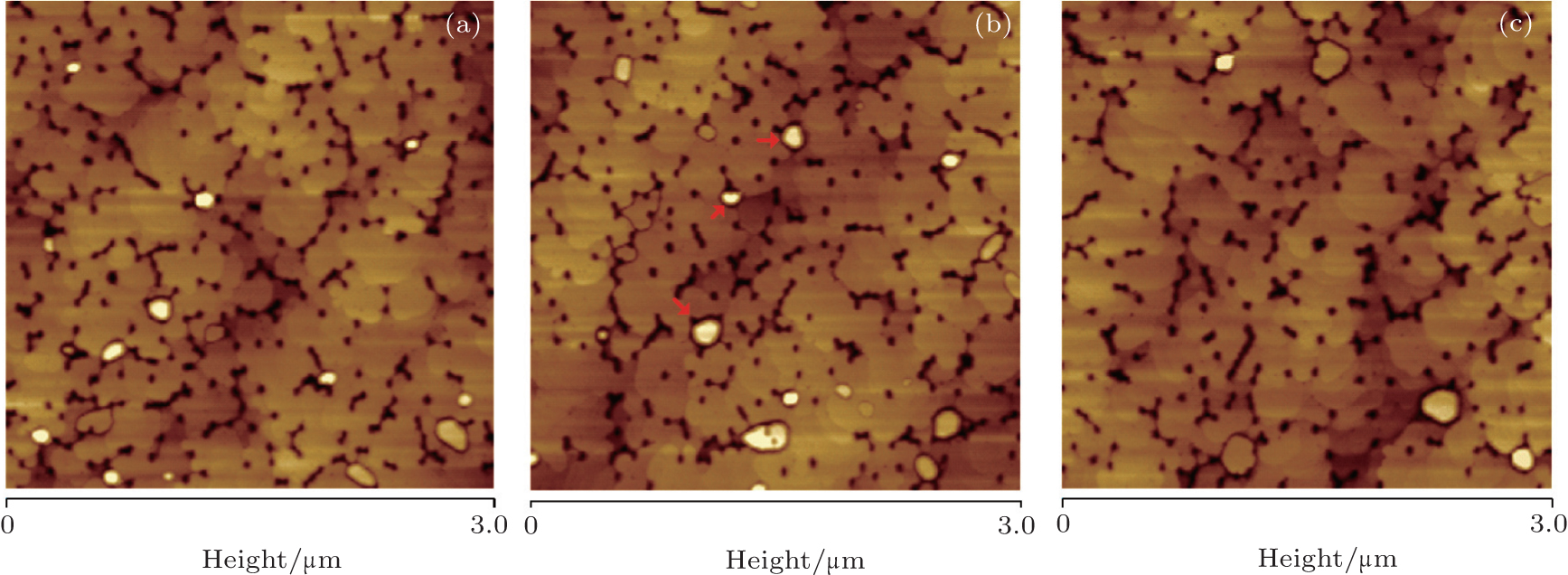
| AFM surface morphology of (a) sample M1, (b) sample M2, (c) sample M3, scan size: 3 μm×3 μm; microstructures indicated by arrows are indium-rich clusters formed in V-pits. |
 |