†Corresponding author. E-mail: qwsong@xidian.edu.cn
*Project supported by the National Natural Science Foundation of China (Grant Nos. 60876061 and 61234006), the Natural Science Foundation of Shaanxi Province, China (Grant No. 2013JQ8012), and the Doctoral Fund of the Ministry of Education of China (Grant Nos. 20130203120017 and 20110203110010).
The non-ideal effect of 4H–SiC bipolar junction transistor (BJT) with a double Gaussian-doped base is characterized and simulated in this paper. By adding a specific interface model between SiC and SiO2, the simulation results are in good agreement with the experiment data. An obvious early effect is found from the output characteristic. As the temperature rises, the early voltage increases, while the current gain gradually decreases, which is totally different from the scenario of silicon BJT. With the same effective Gummel number in the base region, the double Gaussian-doped base structure can realize higher current gain than the single base BJT due to the built-in electric field, whereas the early effect will be more salient. Besides, the emitter current crowding effect is also analyzed. Due to the low sheet resistance in the first highly-doped base epilayer, the 4H–BJT with a double base has more uniform emitter current density across the base-emitter junction, leading to better thermal stability.
Due to the superior properties of silicon carbide (SiC), power devices based on 4H– SiC have been extensively developed in recent years.[1– 3] Compared with other power switching devices, the 4H– SiC BJT has advantages in high voltage with low specific on-resistance due to the conductivity modulation and high current capability. High current gain and high open base breakdown voltage devices have been fabricated, [4, 5] and some novel structures have also been verified.[6, 7] Among them, the double base design can form p-type Ohmic contact to the base without ion implantation, which could eliminate the lattice damage brought by the implantation. For the application, matrix converter and high power dc– dc converter based on 4H– SiC BJTs[8, 9] show excellent performance compared with the silicon IGBT module. In addition, the reliability is still important for 4H– SiC BJTs. In this paper, based on our fabricated 4H– SiC BJTs with double Gaussian-doped base, simulation is executed and the results are compared with the experimental results based on the relevant models. The influences of the early effect and emitter current crowding are studied and the mechanism is discussed. The influences of temperature and doping concentration on the characteristics of the 4H– SiC BJT are also investigated. Moreover, the differences on these two non-ideal effects the between double base structure and the traditional single base structure are compared and analyzed.
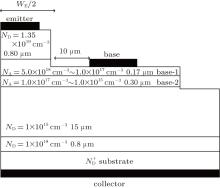
Figure 1 shows a cross section view of the fabricated 4H– SiC BJT with a double Gaussian-doped base. The device was formed on an n-type 3-in (1 in = 2.54 cm) 4° off-axis 4H– SiC substrate with the reactor of the Epigress VP508 hot wall CVD system. Pure nitrogen and tri-methyl-aluminium (TMA) were used as dopants for n-type and p-type epilayers, respectively. SiH4 and C3H8 were adopted as source gases for Si and C, and the C/Si ratio was kept at 1. The growth process started with a buffer layer for 10-min growth and nitrogen doped at a concentration of around 1 × 1018 cm− 3, followed by a 3-h unintentionally doped growth for the drift n-epilayer. The base was grown as a two-layer structure by controlling the mass flow controller (MFC) valves of TMA. The top Gaussian-doped base layer had a high doping concentration to improve the Ohmic contact. Finally, an 800-nm thick emitter layer was grown with a nitrogen concentration of 1.35 × 1019 cm− 3.
The device fabrication started with the emitter finger formation by inductively coupled plasma etching, followed by the device isolation etching. Then, the surface passivation was performed by thermal oxidation and thick SiO2 deposition. Finally, the contact metal was formed by sputtering and rapid thermal processing. More fabrication details have already been presented in Ref. [10]. The measurements were performed using an HP 4156B semiconductor parameter analyzer.
To investigate the non-ideal effects, TCAD simulation was also employed. The main physical models used are shown as follows.
(i) Incomplete ionization by kimoto, [11] in which dopant ionization energy of 61 meV and 200 meV for n-type (nitrogen) and p-type (aluminum) were adopted, respectively.
(ii) Auger recombination by Galeckas, [12] in which the Auger coefficients for electrons and holes were 5 × 10− 31 cm6/s and 9.9 × 10− 31 cm6/s, respectively.
(iii) Bandgap narrowing by Lindefelt, [13] in which the band edge displacement Δ Eg equals 0.08878 eV calculated by the given formulas.
(iv) Shockley– Read– Hall (SRH) recombination considering τ n = 50 ns, τ p = 10 ns, doping concentration (Nreff = 3 × 1017 cm− 3) and temperature dependence (α = 1.72).[14]
(v) Mobility model with doping and high field dependence.[15]
(vi) The specific contact resistances are considered. According to the measurement result by the transmission line method (TLM), the emitter and base specific contact resistances are 6 × 10− 5 Ω · cm2 and 8.7 × 10− 3 Ω · cm2, respectively, while the collector specific contact resistance of 5 × 10− 4 Ω · cm2 was adopted by considering the doping concentration of the n-type substrate.
(vii) SiC/SiO2 interface model by Buono, [16] using one single energy level at 1 eV above the valence band, a capture cross section of 1 × 10− 15 cm2, and a constant trap concentration of 2.49 × 1013 cm− 2· eV− 1.
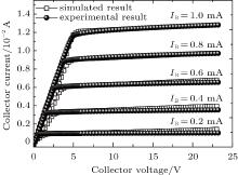
With the device structure and physical models presented above, output characteristics are simulated and the simulation results are compared with the measurement results. Figure 2 shows the common-emitter I– V curves of a single finger device with the base driving current varying from 0.2 mA to 1.0 mA at room temperature. It is verified that the quality of the SiC/SiO2 interface along the base-emitter sidewall is a limiting factor for the current gain.[16] The base current (IB) can be described as follows:

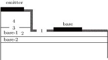
where each composition is displayed in Fig. 3. It contains: 1) surface recombination between SiC/SiO2, namely IRS; 2) carrier recombination in the base bulk, namely IRB; 3) recombination in the space charge region of the BE junction, namely IR; 4) carrier recombination in the emitter bulk, namely IpE. A high concentration of the SiC/SiO2 interface traps could cause high surface recombination in the base, which will increase the base current. Consequently, the current gain comes down. There is no special treatment for the thermal oxidation layer in our experiment, such as NO or N2O annealing[17] and deep level-reduction process, [4] resulting in a high interface state density between SiC and SiO2. In the simulation setup, interface model with a constant trap concentration of 2.49 × 1013 cm− 2· eV− 1 makes the simulated results fit the experimental results satisfactorily as shown in Fig. 2.
Besides, it can also be seen in Fig. 2 that the collector current increases slightly with the increase of the collector voltage from 5 V to 23 V, owing to the early effect in bipolar junction transistors. In other words, the early effect will cause an unsaturated output curve, leading to the variation of the maximum current gain as shown in Fig. 4. This is due to the reduction of the neutral base region caused by the depletion region broadened to the base side of the BC graded junction. In the simulation, the ionized acceptor concentration in the base-2 region NA2(x) is described by the Gaussian distribution, as shown in Eq. (2)[18]

where Cpeak is the peak concentration, d is the distance from peak concentration to the interface of the BC junction, and σ is the standard deviation which is determined by Eq. (3)

In Eq. (3), ydepth and ypeak are the vertical positions of the BC junction interface and peak concentration, respectively, Cdepth is the acceptor concentration at the BC junction interface. The depletion width WB for BC junction on the base side can be expressed by the following equation:[19]

where λ = σ 2, is a characteristic length, VCB is the applied voltage between the collector and the base. Equation (4) shows the relationship between the depletion width WB and the applied voltage VCB. It can be seen from Eqs. (3) and (4) that Cpeak and Cdepth have important influences on WB.
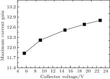 | Fig. 4. Maximum current gain versus collector voltage, extracted from Fig. 2. |
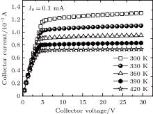
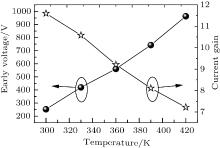
Furthermore, the I– V characteristics at different temperatures with a certain IB (1.0 mA) are also investigated. The range is from room temperature to about 150 ° C as shown in Fig. 5. It is known that the aluminum acceptors in 4H– SiC are not fully ionized even at high temperature due to the high ionization energy. As the temperature rises, the ionized acceptor concentration in the base region will increase exponentially. For doping concentrations of 1 × 1017 cm− 3 and 1 × 1018 cm− 3, the ionization rates will increase from 15% and 5% to 47% and 19%, respectively, when temperature rises to 150 ° C.[11] According to Eq. (4), the increased ionized acceptors have a great influence on reducing the depletion width of the BC junction at the base side. As a consequence, the neutral base width and early voltages increase, leading to a better saturation characteristic and current gain stability. On the contrary, unlike the silicon BJT, the maximum current gain will decrease gradually as temperature increases due to the reduction of the local emitter-injection coefficient and the base transport factor as shown in Fig. 6.
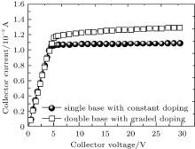
From the analysis above, it can be seen that the doping concentration of the base region is a limiting factor for early voltage and the current gain. To investigate the effect of the doping profile, a 4H– SiC BJT with single base structure and constant doping, which has the same effective Gummel number as the double base 4H– BJT, is also simulated. Figure 7 shows a comparison of the I– V curve between a single base BJT and a double Gaussian-doped BJT with a certain IB (0.1 mA) at room temperature. The Gummel number is 5.89 × 1013 cm− 2 calculated with the results measured from the secondary ion mass spectroscopy (SIMS). Extracted from the curves, the early voltage of the single base BJT is 1735.91 V, which is seven times the double base BJT’ s. This is due to the really high doping concentration of the base (1018 cm− 3) which makes the depletion edge of the BC junction almost exclusively spread to the collector region. However, the current gain of the double base BJT is much higher, which is due to the built-in electric field accelerating the transport of the electron in the base region.[6, 10]
It has been demonstrated that the concentration difference between the two base layers has a positive effect on the built-in electric field. However, a high doping concentration of the base-1 region will reduce the local emitter-injection coefficient, while a low doping concentration of the base-2 region may aggravate the early effect. According to the analysis, it is believed that the doping concentration in the base-2 region next to the BC junction (NA2J), which is 1 × 1015 cm− 3 in the fabricated device, is an important parameter for the early voltage. Table 1 shows the simulated current gain and the early voltage for different values of NA2J, i.e., 5 × 1015 cm− 3, 1 × 1016 cm− 3, 5 × 1016 cm− 3, and uniform-doped in base-2 region with a concentration of 1 × 1017 cm− 3. There is a trade-off between the current gain and the early voltage. To reduce the early effect, constant doping with a concentration of 1 × 1017 cm− 3 in the base-2 region is preferable.
| Table 1. Simulated current gains and early voltages with different values of NA2J. |
Before the device fabrication, the thickness and doping concentration in the base-1 region are optimized. An orthogonal experiment is performed to achieve high current gain by employing the thickness and doping concentration in base-2 as key factors. In addition, realizability of processes such as Ohmic contact and epitaxial growth is also considered. As a result, thickness varying from 0.15 μ m to 0.18 μ m and doping concentration varying from 4.6 × 1018 cm− 3 to 5.0 × 1018 cm− 3 are chosen as suitable parameters for the base-1 region.
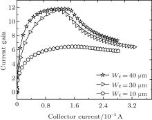
Comparisons of the simulated results of the current gain for two different emitter widths with the experimental data are presented in Fig. 8, in which all experimental results are measured on single finger BJT. The curves shows that the simulated results coincide with the experimental data, which is due to the non-uniformity quality between SiO2 and SiC on the whole wafer. A possible trend is also found that the current gain increases with the increase of the emitter width. To confirm this, one more simulation result with an emitter width of 40 μ m is added in Fig. 9. However, the current gain tends to be saturated. This phenomenon has also been proved in Refs. [20] and [21]. The high resistance in the base region makes the current unsuccessfully flow to the center of the emitter region. Thus, although the emitter width increases, it has no change in the effective active area. Obviously, the geometric design is a very important issue for 4H– SiC BJTs.
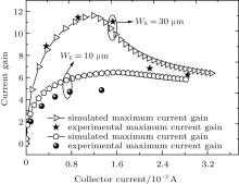 | Fig. 8. Comparisons of the simulated current gain with experimental results for different emitter widths. |
In order to study the influence of the base resistance, the electrostatic potential along the horizontal direction in the top base region is shown in Fig. 10, in which the performance of single base structure is also included for comparison. Due to an order of magnitude difference in the acceptor concentration, 4H– SiC BJT with double base has a more uniform distribution of the electrostatic potential, leading to smooth current density under the active area. The relationship between the emitter current density (JE) and the electrostatic potential of the BE junction (VBE) is determined as follows:[22]

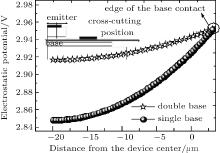 | Fig. 10. Distributions of the electrostatic potential in the base region on forward bias. |
As shown in this equation, a slight change of the VBE will cause a great variation of JE. Taking it for example in Fig. 10, the electrostatic potential of the center and the edge of the base contact in single base structure are 2.85 V and 2.95 V, respectively. Calculated according to Eq. (5), the current density of the edge of the base contact is almost 48 times the center’ s, which shows an obvious emitter current crowding effect. However, the current density of the edge of the base contact is only 3 times the center’ s in the double structure, indicating more uniform current distribution in the base region.
In this study, based on our fabricated 4H– SiC BJT with double Gaussian-doped base, the non-ideal effects including the early effect and emitter current crowding are investigated by comparing the accurate simulated results with measured data. Compared with the conventional 4H– SiC BJT with a single base, the double base device has a better performance on the current gain and current uniformity under the active area. However, the early effect is more obvious due to the low doping concentration of base-2 region next to the base-collector junction. With temperature increasing, the effect will become weaker, indicating that 4H– SiC BJTs is more suitable for the high temperature application.
| 1 |
|
| 2 |
|
| 3 |
|
| 4 |
|
| 5 |
|
| 6 |
|
| 7 |
|
| 8 |
|
| 9 |
|
| 10 |
|
| 11 |
|
| 12 |
|
| 13 |
|
| 14 |
|
| 15 |
|
| 16 |
|
| 17 |
|
| 18 |
|
| 19 |
|
| 20 |
|
| 21 |
|
| 22 |
|


