†Corresponding author. E-mail: huming@tju.edu.cn
*Project supported by the National Natural Science Foundation of China (Grant No. 61235011) and the Science Foundation of the Science and Technology Commission of Tianjin Municipality, China (Grant Nos. 13JCYBJC17300 and 12JCQNIC01200).
Diamond-like carbon (DLC) thin film is one of the most widely used optical thin films. The fraction of chemical bondings has a great influence on the properties of the DLC film. In this work, DLC thin films are prepared by ion-beam sputtering deposition in Ar and CH4 mixtures with graphite as the target. The influences of the ion-beam voltage on the surface morphology, chemical structure, mechanical and infrared optical properties of the DLC films are investigated by atomic force microscopy (AFM), Raman spectroscopy, nanoindentation, and Fourier transform infrared (FTIR) spectroscopy, respectively. The results show that the surface of the film is uniform and smooth. The film contains sp2 and sp3 hybridized carbon bondings. The film prepared by lower ion beam voltage has a higher sp3 bonding content. It is found that the hardness of DLC films increases with reducing ion-beam voltage, which can be attributed to an increase in the fraction of sp3 carbon bondings in the DLC film. The optical constants can be obtained by the whole infrared optical spectrum fitting with the transmittance spectrum. The refractive index increases with the decrease of the ion-beam voltage, while the extinction coefficient decreases.
Diamond-like carbon (DLC) film has been widely investigated[1– 6] because of its high mechanical hardness, high electrical resistivity, and excellent optical transparency over a wide range. The film is comprised of a mixture of sp3 and sp2 hybridized carbon bondings.[7– 9] The electrical, optical, and mechanical properties of DLC can be tuned by varying the fraction of sp3 and sp2 hybridized carbon in the film.[10– 13]
There are many methods of depositing DLC thin films including chemical vapor deposition, [14, 15] magnetron sputtering deposition, [16, 17] pulsed laser deposition, [18, 19] etc. Ion-beam sputtering deposition has also been used in a number of studies aiming to obtain high-quality optical film which has a uniform and smooth surface, high density, and low optical absorption.[20, 21] In recent years, some researchers have deposited DLC films by ion-beam sputtering deposition. Meš kinis et al.[22] prepared undoped and SiOx-doped DLC thin films by varying systematically the gas content, and they investigated the doping effect to satisfy criteria for high temperature embossing and UV assisted molding. Rybachuk and Bel[23] investigated the suitability of a single ion-beam deposition method for fabricating the DLC films and the effects of the positioning of a substrate at grazing angle on structural changes in the films. However, there are very few reports about the influences of deposition parameters on the surface morphology, chemical bonding, optical and mechanical properties of DLC films prepared by ion-beam sputtering deposition.
In this work, the DLC films are prepared by ion-beam sputtering a pure graphite target in a CH4/Ar mixture. The surface morphology, chemical bonding, mechanical and optical properties are investigated as a function of ion-beam voltage. The intrinsic correlations between the chemical bonding and properties of the DLC film are illustrated.
The DLC films were deposited on polished Si and Ge substrates by ion beam sputtering deposition. High purity graphite (mass fraction: > 99.995%) was selected as a target material. The deposition chamber was set at a base pressure less than 1× 10− 3 Pa. High-purity CH4 (volume fraction: > 99.99%) was introduced on the surface of the target material in the deposition process. High-purity Ar (volume fraction: > 99.999%) as the working gas was introduced into the sputtering ion source. The ion beam voltages were 600 V, 1000 V, and 1200 V, respectively. The ion-beam current was 400 mA. The Ar and CH4 flows were both 32 sccm. The working pressure was about 4× 10− 2 Pa. The DLC thin films were deposited at ambient temperature.
The root-mean squared (RMS) roughness and morphology were investigated with a Nanosurf easyscan 2Flex atomic force microscope operating in tapping mode. Raman spectrum of the deposited film was measured using a DXR Raman microscope with the laser line at 532 nm. The film hardness was described by nanoindentation measurement (Nano Indenter G200, Agilent Tech.), and the Berkovich indenter was chosen during testing. The transmittance of the sample in a range of 1500 nm– 10000 nm was obtained by an FTIR spectroscope (PE spectrum GX). The thickness and optical constants of the sample were determined from the whole infrared optical spectrum fitting with the transmittance spectrum. The DLC films deposited on Si substrates were used for AFM, Raman, and nanoindentation measurements. In order to avoid the strong absorption from the silicon substrate, the DLC films deposited on the Ge substrates were used for the FTIR test.
To investigate the application of the DLC film as antireflective and protective film, the DLC film and antireflective films were deposited on the front side and back side of the Si substrate, respectively. The DLC film was deposited at an ion-beam voltage of 600 V. The thickness of the DLC film was 468 nm. The structure of the antireflective film on the back side was Al2O3/Ge/Al2O3. The Al2O3 film and Ge film were prepared by electron beam evaporation. The base pressure was less than 1× 10− 3 Pa. The temperature of the substrate was 200 ° C. The growth rates of the Al2O3 film and Ge film were 0.3 nm/s and 0.4 nm/s, respectively. The thickness values of each layer in the Al2O3/Ge/Al2O3 structure were 111 nm, 113 nm, and 698 nm, respectively.
AFM images of DLC thin films prepared with different ion-beam voltages are shown in Fig. 1. The DLC thin films show some small particles on the surface. The surfaces of all the films are quite uniform and smooth. The surface roughness values of the DLC films are 2.403 nm, 2.265 nm, and 1.866 nm, respectively. As the ion-beam voltage increases from 600 V to 1200 V, the surface roughness value decreases, which indicates that higher ion-beam voltage is more likely to facilitate the preparation of DLC films with smaller surface roughness.
The Raman spectrum is an effective way to obtain quantitative information about the sp2 and sp3 hybridized carbon bondings in the film. The Raman spectra for the DLC films measured in a range of 900 cm− 1– 2000 cm− 1 are shown in Fig. 2. A broad peak between 1000 cm− 1 and 1800 cm− 1 is observed. The broad peak is considered as a combination of G peak associated with the symmetric E2g vibrational mode in graphite-like material and D peak which is attributed to disorder-allowed phonon modes.[24, 25]
The spectra can be fitted by Gaussian curves. It is shown that the positions of D and G peaks (ω D and ω G) are at approximately 1370 cm− 1 and 1550 cm− 1, respectively. The positions and intensity ratio (ID/IG) of two bands obtained from this fitting procedure are listed in Table 1.
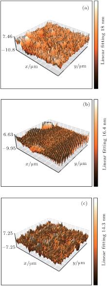 | Fig. 1. The AFM images of the DLC films deposited at different ion-beam voltage: (a) 600 V, (b) 1000 V, and (c) 1200 V. |
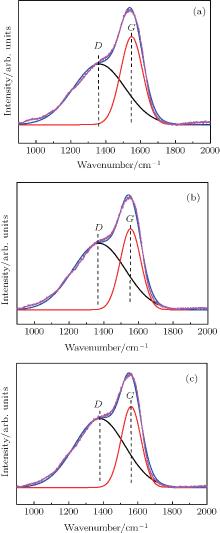 | Fig. 2. Raman spectra for the DLC films deposited at different ion-beam voltages (a) 600 V, (b) 1000 V, and (c) 1200 V. |
| Table 1. Positions (ω D and ω G) and intensity ratio (ID/IG) of two bands for DLC films deposited at different ion-beam voltages. |
It can be seen from Table 1 that the position of the G band shifts toward a higher wavenumber with the increase of ion-beam voltage. Meanwhile, the intensity ratio (ID/IG) increases with increasing ion-beam voltage. It can be concluded that the fraction of sp3 carbon bondings in the film decreases with the increase of ion-beam voltage. Sputtering of the graphite target and decomposition of the CH4 are both important processes in the deposition of the DLC film. The carbon atoms sputtered from the graphite are more likely to form sp2-hybridized carbon bondings. Higher content of the sp2-hybridized carbon bondings will reduce the hardness and enhance the absorption of the film. The CH4 is a molecule with the tetrahedron structure. The carbon atoms decomposed from the CH4 tend to form sp3 bondings. It was reported that as the hydrogen in the gas phase decomposed from the CH4 facilitates the formation of the sp3 carbon structure, [26] the fraction of the sp3-hybridized carbon bondings in the DLC film could increase by promoting the decomposition of the CH4. However, as the ion-beam voltage increases, the energy of Ar ions used for sputtering increases, which leads to increasing the sputtering rate of the graphite. It could facilitate the formation of the sp2-hybridized carbon bondings, resulting in the decrease of the fraction of sp3-hybridized carbon bondings.
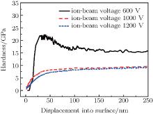
Figure 3 displays the hardness values of the DLC films prepared at different ion-beam voltages. It can be seen that as ion-beam voltage increases, the hardness of the film decreases monotonically. As mentioned above, the DLC film deposited at lower ion-beam voltage has higher sp3-hybridized carbon atom density. It makes the DLC network more similar to that of diamond at lower ion-beam voltage. A higher fraction of sp2 carbon bondings may cause the formation of the structure to be more similar to that of graphite. Hence, the decrease in hardness of the DLC film with increasing ion-beam voltage can be due to a transformation in the microstructure for DLC film from diamond-like to graphitic-like structure.[27]
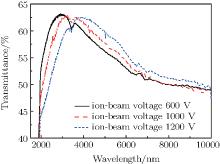
Figure 4 shows the FTIR spectra of the DLC film deposited on Ge substrate at ion-beam voltages in a range of 1500 nm– 10000 nm. It is shown that with the increase of ion-beam voltage, the transmittance decreases. In addition, as the ion-beam voltage increases, the position of the peak in the spectrum shifts toward a long wavelength. It can be inferred that the optical thickness of thin film increases with increasing ion-beam voltage. It can also be seen that there are absorption peaks at 3400 nm and 7300 nm for all the DLC films. The peaks can be attributed to the sp3 C– Hn bonds and sp2 C= C bonds, [15, 28] respectively. The density of sp2 C= C bonds becomes higher with increasing ion-beam voltage, while the density of sp3 C– H bonds turns lower with increasing ion-beam voltage.
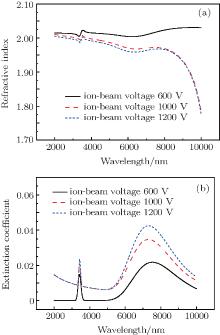 | Fig. 5. Optical constants of the DLC films: (a) refractive indices, and (b) extinction coefficients. |
Figure 5 shows the optical constants obtained by fitting to the transmittance spectrum. The dispersion characteristics of the optical constants of DLC films are obviously seen. The thickness values of the films deposited at 600 V, 1000 V, and 1200 V are 365 nm, 411 nm, and 474 nm, respectively. Due to strong absorptions at 3400 nm, and 7300 nm, there are some peaks at the same position in the dispersion curves of the optical constants. It can be seen that the film prepared by lower ion-beam voltage exhibits a higher refractive index in the whole spectral range. The extinction coefficient of DLC film is low, which is of practical significance for designing and preparing multilayer IR coatings. The extinction coefficient decreases with the decrease of the ion-beam voltage. As mentioned in Subsection 3.2, the fraction of sp3 carbon bondings in the film increases with the decrease of ion-beam voltage. The relatively high fraction of sp3 carbon bondings can result in a higher refractive index and lower extinction coefficient.
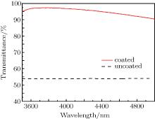
Figure 6 shows the FTIR spectra of the Si substrate coated with the DLC film and antireflective film in a range of 3500 nm– 5000 nm. It can be seen from Fig. 6 that the transmittance for the Si substrate is greatly improved in the range of 3500 nm– 5000 nm. The average value of the transmittance is 95.1%. The result suggests that the DLC film with good optical properties has the potential to be used as an antireflective and protective film.
DLC films are prepared by ion-beam sputtering of a high-purity graphite target at different ion-beam voltages in a CH4/Ar mixture. The ion-beam voltage has a great influence on the properties of the DLC film. The surface of the DLC film is very smooth. The content of sp3 carbon in the film decreases with ion-beam voltage increasing from 600 V to 1200 V. It leads to a consistent decrease in the hardness of DLC films with increasing ion beam voltage. It is found that the refractive index of DLC films decreases, while the extinction coefficient increases with increasing ion-beam voltage from 600 V to 1200 V, which can be attributed to a decrease in the sp3 carbon content of the DLC film. Furthermore, the transmittance values of DLC film and antireflective film-coated Si substrate are tested. The transmittance for the Si substrate is greatly improved in the wavelength region of 3500 nm– 5000 nm.
| 1 |
|
| 2 |
|
| 3 |
|
| 4 |
|
| 5 |
|
| 6 |
|
| 7 |
|
| 8 |
|
| 9 |
|
| 10 |
|
| 11 |
|
| 12 |
|
| 13 |
|
| 14 |
|
| 15 |
|
| 16 |
|
| 17 |
|
| 18 |
|
| 19 |
|
| 20 |
|
| 21 |
|
| 22 |
|
| 23 |
|
| 24 |
|
| 25 |
|
| 26 |
|
| 27 |
|
| 28 |
|


