1. IntroductionThe transition metal chalcogenides have been a fertile land for studying new phenomena and properties in condensed matter physics, including the traditional study of charge density wave (CDW) and related superconductivity[1, 2] and the latest discovery of three-dimensional topological insulators.[3– 5] Among them, a number of MX2-type transition metal dichalcogenides, including IrTe2, WTe2, MoS2, and MoSe2, have attracted great attention recently due to their rich physical properties like charge-density wave, [6– 8] superconductivity, [9– 13] catalysis of chemical reactions, [14] pressure-induced structural rearrangement, [15] extremely large magneto-resistance, [16, 17] and potential technological applications.[16, 18– 22] There is still plenty of room to explore for new phenomena and physical properties in the transition metal dichalcogenides, particularly in those systems that have been paid less attention before, such as the systems consisting of the VIII metal and chalcogen atoms such as PdTe2, NiTe2, PtSe2, PtS2, and so on. The Pd– Te system can form various intermetallic compounds like PdTe2, PdTe, Pd3Te2, and Pd4Te.[23– 35] Among them, the most studied CdI2-type PdTe2 and NiAs-type PdTe are superconductors with Tc of 1.7 K[12, 36] and 2.3 K– 4.5 K, [25, 26, 31, 37] respectively. Understanding the electronic structures of these compounds is important for understanding the related superconductivity mechanism and exploring for new phenomena and physical properties.
In this paper, we focus on the investigation of the electronic structures of PdTe2 and its Cu-intercalated counterpart Cu0.05PdTe2. Few work has been reported in the literature except for some earlier scanning tunneling spectroscopy[38, 39] and angle-resolved photoemission studies on PdTe2.[40] We carried out systematic high resolution angle-resolved photoemission (ARPES) measurements on the electronic structures of PdTe2 and Cu0.05PdTe2. Multiple bands with strong dispersions are revealed over a wide energy range (0 eV– 6 eV), which give rise to a complex Fermi surface topology. We also performed detailed band structure calculations for PdTe2 by considering the spin– orbit coupling effect. The calculated band structure exhibits strong three-dimensionality. The comparison with the theoretical calculations facilitates the assignment of the observed band structure and Fermi surface, with some observed features not accounted for in the bulk band calculations. While the overall electronic structure is similar between PdTe2 and Cu0.05PdTe2, some delicate differences are identified. In particular, there is a downshift of the band on the order of 16 meV observed in Cu0.05PdTe2, indicating the electron doping from Cu-intercalation in the system.
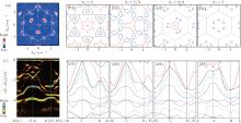
3. Results and discussionFigure 1 shows the crystal structure and the corresponding Brillouin zone of the parent compound PdTe2, as well as the characterization information of the intercalated Cu0.05PdTe2 single crystal. The crystal structure of PdTe2 (Fig. 1(a)) is polymeric CdI2-type with the P3m1 (No. 164) space group.[6, 15, 43, 44, 46] The palladium atom is octahedrally coordinated by six tellurium atoms. Each Pd– Te layer consists of a two-dimensional close-packed array of palladium atoms sandwiched between two similar arrays of tellurium atoms.[10, 12, 47] Within the layer, the atoms are covalently bonded, while between the layers, they are bonded weakly in the van der Waals style. Thus the crystal can be easily cleaved between the layers. The corresponding Brillouin zone is a hexagonal prism as shown in Fig. 1(b). Magnetization measurement of the Cu0.05PdTe2 crystal was done in the field-cooled (FC) and zero-field-cooled (ZFC) modes with a magnetic field of 1 Oe (1 Oe = 79.5775 A· m− 1), giving a superconducting transition temperature Tc ∼ 2.4 K (Fig. 1(c)), which is obviously higher than that of the parent compound PdTe2 (Tc∼ 1.7 K).[12, 36] The dimension of the single crystal is about 5 mm× 3 mm× 0.2 mm, with a shining surface as shown in the inset of Fig. 1(c). Single crystal x-ray diffraction was carried out on the Cu0.05PdTe2 sample (Fig. 1(d)). The observed peaks can be indexed into (0 0 n) (with n being integers), indicating that the naturally cleaved surface is the basal plane. Based on the Laue diffraction pattern shown in Fig. 1(e), we can determine the orientation of the crystal. The low-energy electron diffraction (LEED) pattern on the cleaved surface taken at 25 K at the electron energy of 70 eV is shown in Fig. 1(f). It is consistent with our Laue measurement. The pattern of sharp and bright spots demonstrates a three-fold symmetry; no surface reconstruction is observed.
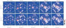
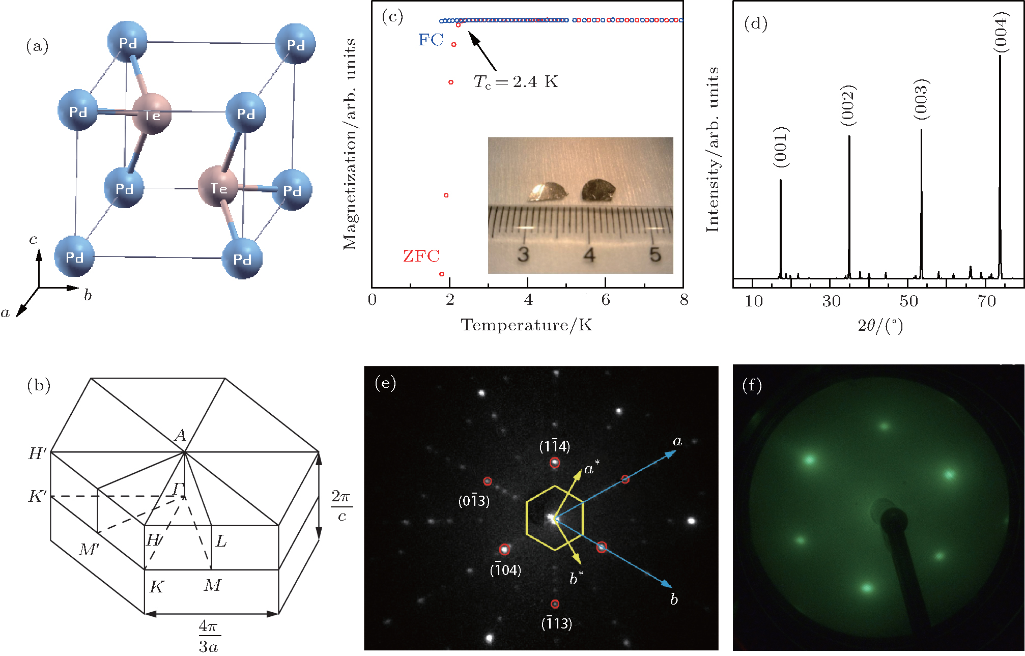
Figure 2 shows the constant energy contours of the ARPES spectral weight distribution for both PdTe2 (Fig. 2(a)) and Cu0.05PdTe2 (Fig. 2(b)) at different binding energies. Overall speaking, the constant energy contours of PdTe2 and Cu0.05PdTe2 samples are quite similar; they both evolve strongly with the binding energy. Near the Fermi level, both compounds exhibit a complex Fermi surface topology with a three-fold symmetry. A couple of main features can be well resolved. A small electron-like spot appears around the Γ point, denoted as α . It is surrounded by six small electron-like spots (β and β ′ ) located near the midpoint between Γ and K. There is a rather weak spectral weight that links in between the β and β ′ spots. There is also a weak spectral weight extending out from each β spot to the M and M′ points, marked as δ and δ ′ bands, respectively. These observations show some resemblance to that found in the parent IrTe2[48] and doped Ir0.95Pt0.05Te2[49] single crystals. Although in that case, the six inner hole pockets are six-fold symmetric. Right outside the first Brillouin zone boundary, there appear two flap-like sheets (denoted as γ and γ ′ ) popping out symmetrically with respect to the Γ – K and Γ – K′ lines, respectively. They also exhibit the three-fold symmetry. Going further into the second zone, more complicated features appear. With the increasing binding energy, the α spot near the Γ point shrinks, while the three β and three β ′ spots near the Γ – K and Γ – K′ middle points first diminish quickly and then reemerge gradually to become warped square pockets (Figs. 2(a2)– 2(a5) and Figs. 2(b2)– 2(b5)). Near the K (K′ ) regions, the two flap-like γ features at the Fermi level move away from the K (K′ ) points and disappear quickly with increasing binding energy while another two big pockets approach to the K (K′ ) points (Figs. 2(a4), 2(a5), 2(b4), and 2(b5)). We note that, in both compounds, the measured electronic structure in the second Brillouin zone does not reproduce that in the first Brillouin zone. This may be caused by the strong momentum-dependent photoemission matrix-element effect that can alter the relative spectral intensities of various bands. It is also possible that this is due to the strong three-dimensionality of the measured materials, i.e., the band structures show strong kz dependence, as we will see below from the band structure calculations. For ARPES with a given photon energy of 21.2 eV, the covered momentum space is a curved surface with different kz, which can be obviously different between the first and the second Brillouin zones.
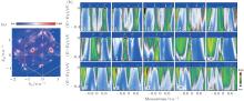
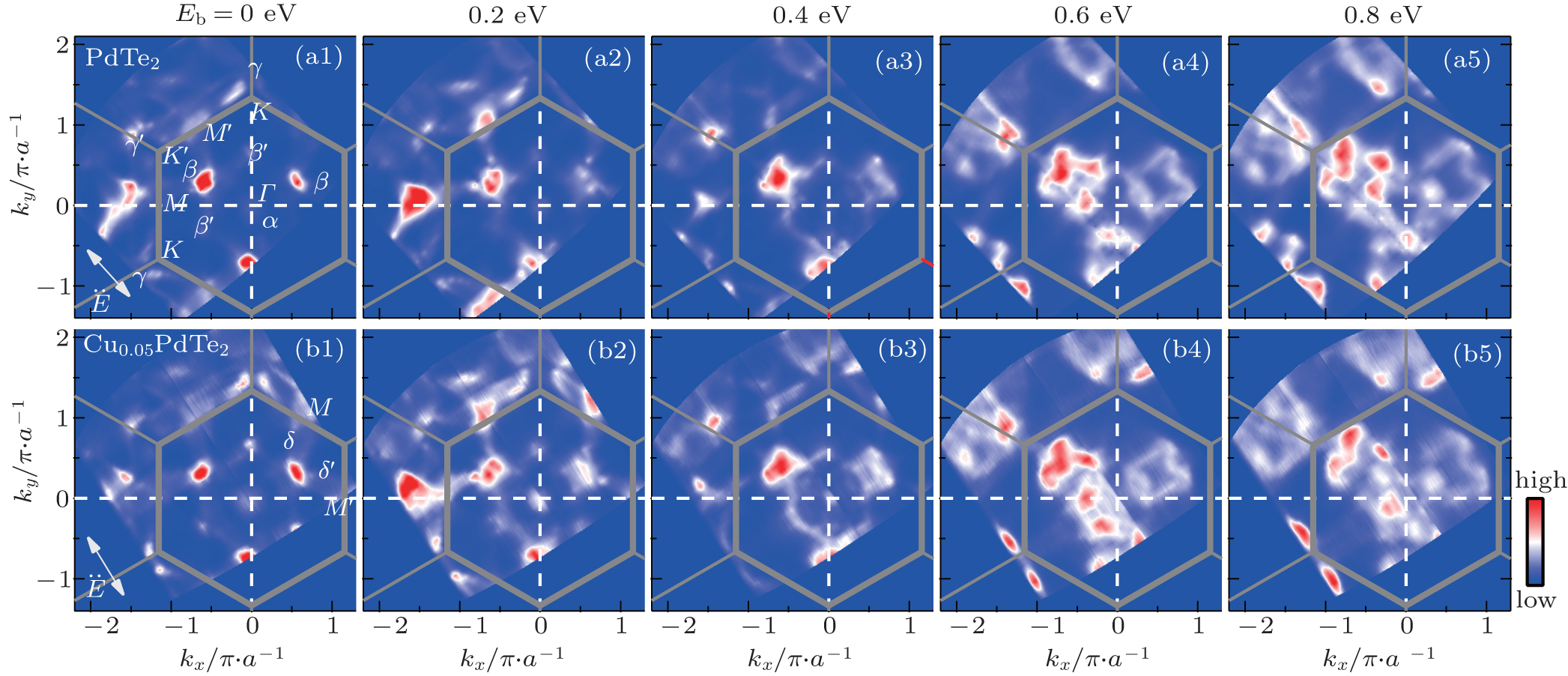
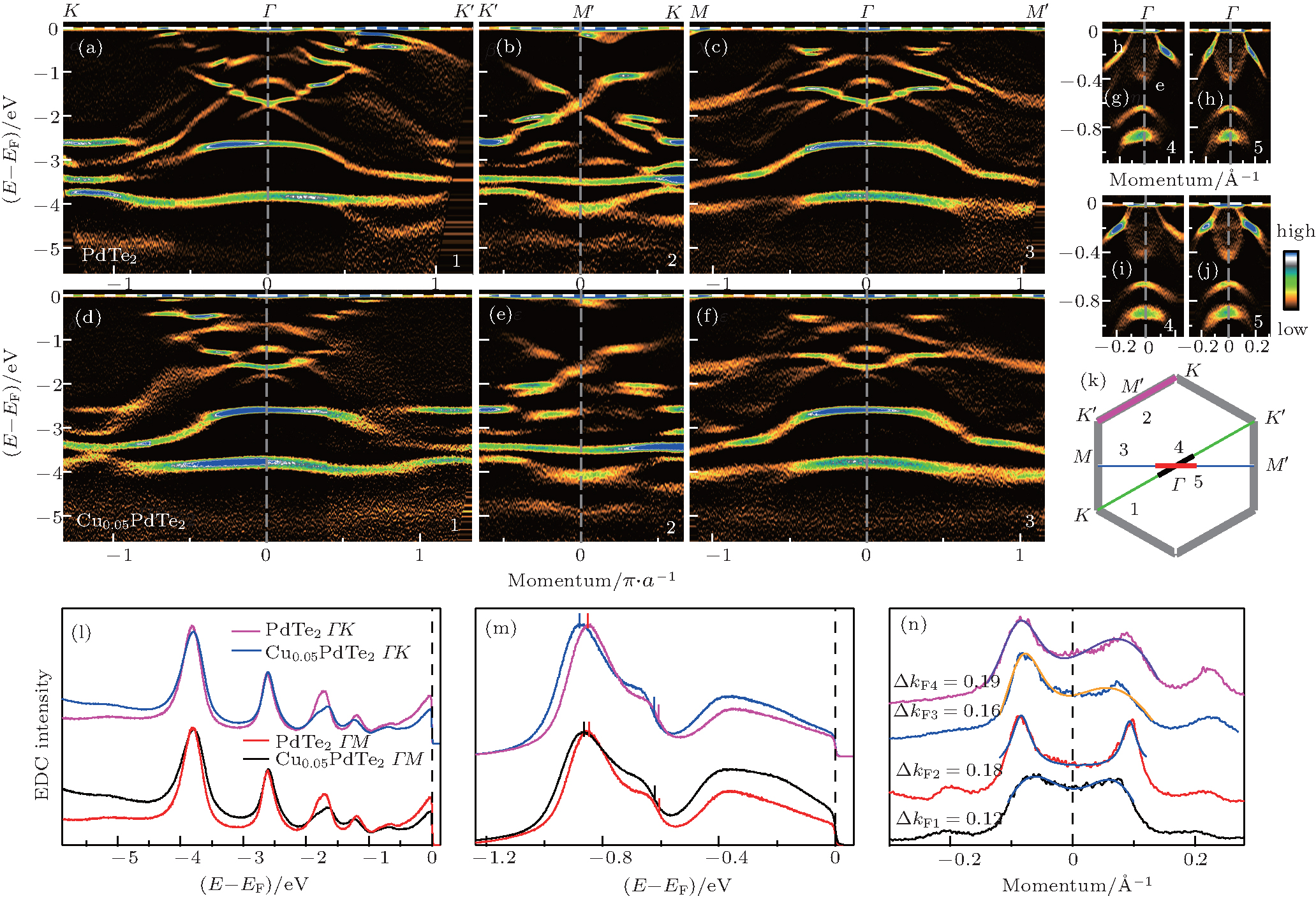
Figure 3 shows the overall band structure of Cu0.05PdTe2 measured along three high symmetry momentum cuts with their locations marked in Fig. 3(a). Figures 3(b)– 3(d) show the original data, while figures 3(e)– 3(g) show the corresponding second-derivative images with respect to energy in order to better highlight some bands. Multiple dispersive bands are observed within a large energy range up to ∼ 6 eV binding energy that we have covered. These results are consistent with the earlier theoretical calculations[46, 47] and the ARPES work on PdTe2[40] that suggested nine hybridized bands composed of Pd 4d states and Te 5p states. Our new high-resolution ARPES data shown here undoubtedly provide clearer and comprehensive electronic structure information. From Figs. 3(b) and 3(c), near the Fermi level, an electron-like band can be seen at the Γ point, which corresponds to the α -Fermi pocket near Γ in Fig. 3(a). In addition, near the midpoint of Γ – K (K′ ), small electron-like β (β ′ ) bands cross the Fermi level. The subtle difference in the band structures near the Fermi level between Γ – K (Figs. 3(b) and 3(e)) and Γ – M (Figs. 3(c) and 3(f)) accounts for the difference in the Fermi surface topology and the constant energy contours (Figs. 2 and 3(a)) along the two momentum directions. At high binding energies (above 1 eV), the measured band structures along Γ – M and Γ – K look similar qualitatively.
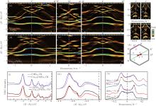
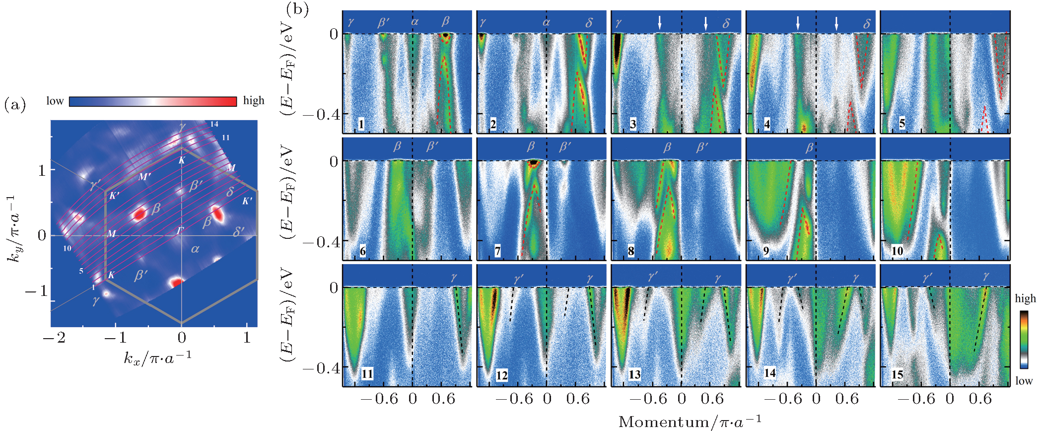
Figure 4 focuses on the low-energy electronic structures of Cu0.05PdTe2 and shows the detailed momentum evolution of the band structures, which helps to understand the features in the measured Fermi surface. Along the representative momentum cut 1, the measured band structure (Fig. 4(b), cut 1) shows four main features: α band near the Γ point, β and β ′ bands sitting near the middle of Γ – K and Γ – K′ , respectively, and γ band just outside of the K point. The α band shows an electron-like parabolic dispersion for cut 1; the band becomes narrower for cut 2 and disappears for cut 3 in Fig. 4(b), indicating a small electron pocket near the Γ point in the measured Fermi surface (Fig. 4(a)). The most prominent β bright spots in the measured Fermi surface (Fig. 4(a)) appear to be singular spots, because they have dramatically high intensities and are localized in a rather small momentum space. Right beneath the β spot, one can identify some narrow and relatively deep hole-like bands. These hole-like bands are responsible for the warped square-like pocket near the same location at higher binding energy, as shown in Figs. 2(a) and 2(b). They are localized in the area around the Γ – K middle points. Even though the β ′ features show rather weak spectral intensity compared with the β bands, the corresponding complex electronic behaviors are quite similar.
Furthermore, several features can grow out from these β and β ′ pockets. First, two groups of bands can extend out from each β (but not β ′ ) pocket towards the adjacent M and M′ points on the zone boundary, symmetric with respect to the Γ – K′ lines, marked as δ and δ ′ bands in Figs. 2(b) and 4(a). These features further connect with some complicated structures in the second Brillouin zone. The evolution of the corresponding bands in Fig. 4(b) (cuts 1– 5) clearly indicates that these δ (δ ′ ) bands are electron-like. From Fig. 4(b), the electron-like δ bands seem to grow naturally from the β bands in terms of band structure evolution. However, the singular behavior of the particularly strong intensity of the β bright spots seems not to be compatible with this evolution. Whether it is the same as the δ band or it comes from a different origin needs to be further investigated. Second, there are also some weak features that link all the β and β ′ points together to form a hexagon centered at the Γ point (Figs. 2 and 4(a)). The measured bands that are responsible for the linking features are marked by the white arrows in Fig. 4 (cuts 3 and 4), showing steep bands crossing the Fermi level. Third, as shown in Fig. 4(b) (cuts 13 and 14), the two wings for the γ (and γ ′ ) bands close to the K (and K′ ) points form a hole-like band around the Brillouin zone boundary line in the second zone. In addition to these three major features, there are other bands that also contribute to the Fermi surface in the second Brillouin zone. All these observations suggest the multiband nature of the PdTe2 system at low energy which should be considered in understanding its superconductivity and related properties. Our present work provides for the first time detailed information on the complex electronic structure of the PdTe2 system.
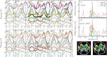
The Tc enhancement in Cu0.05PdTe2 (Tc = 2.4 K) compared to its parent compound PdTe2 (Tc = 1.7 K) prompted us to investigate the change in the electronic structures induced by the Cu intercalation. Figure 5 presents the direct electronic structure comparison between the intercalated Cu0.05PdTe2 (Figs. 5(d)– 5(f), 5(i), 5(j)) and undoped PdTe2 (Figs. 5(a)– 5(c), 5(g), 5(h)) systems measured at ∼ 20 K using both the 21.218-eV and 6.994-eV photon energies. Like the overall similarity of the Fermi surface shown in Fig. 2, the doped and undoped samples share similar band structures to a great detail for the measurements carried out with the same photon energy (Fig. 5). On the other hand, the measured band structure shows a big difference for the same momentum cut between the two different photon energies (compare Figs. 5(a), 5(c), 5(d), 5(f) with Figs. 5(g), 5(h), 5(i), 5(j)). While only a weak electron-like α band is observed near the Γ point near the Fermi level in the 21.2-eV measurements (Figs. 3(b) and 3(c)), both a hole-like narrow band denoted as h-band that crosses the Fermi level, and an electron-like band denoted as e-band are observed in the 6.994-eV laser ARPES measurements (Figs. 5(g)– 5(j)). We notice that, the electron-like e-band here has an energy range from − 0.46 eV to 0 eV, which is consistent with the α band observed in the helium-lamp-based data. However they show a slight difference in the momentum range. A careful examination indicates that the e-band in the laser measurement has a momentum range from − 0.2 Å − 1 to 0.2 Å − 1 at the Fermi level in PdTe2, while it is from − 0.15 Å − 1 to 0.15 Å − 1 for the α band at the Fermi level in the helium lamp measurement. Considering the different momentum resolutions of the two photon energies and the photoemission matrix-element effect, we believe that the e-band observed by the laser ARPES is most likely the α band we identified in the helium lamp measurement. But the hole-like h-band in the laser ARPES measurement is totally absent in the helium lamp measurements. Besides the h-band, there are two other hole-like bands centered at the Γ point in the laser measurement at higher binding energies (0.6 eV– 1.1 eV) which are not observed in the helium lamp experiment. These differences reflect strong kz dependence of the three-dimensional electronic structure for PdTe2, as we will see in the following band structure calculations.
The band structure change induced by Cu-intercalation can be revealed by comparing the core level energy shifts. Figure 5(l) shows the energy distribution curves (EDCs) at the Γ point taken from both the Γ – M and Γ – K momentum cuts for PdTe2 and Cu0.05PdTe2 samples measured by using 21.2-eV photon energy. Although there is a slight relative intensity variation of the observed peaks between these two samples, overall in the large energy range, there is no obvious peak position shift within our measurement precision. On the other hand, using the high resolution vacuum ultra-violet laser ARPES, we can see obvious relative energy shifts in the EDCs at the Γ point between the doped and undoped PdTe2 systems (Fig. 5(m)). The features in the covered energy range for Cu0.05PdTe2 exhibit a shift of ∼ 16 meV towards the high binding energy. This shift can also be corroborated by the change of the distance between the two Fermi momenta kF of the hole-like h-bands at the Fermi level (Fig. 5(n)); it shows a clear shrink (∼ 0.03 Å − 1) for the Cu0.05PdTe2 sample, consistent with the chemical potential shift towards higher binding energy. These observations indicate that Cu-intercalation in PdTe2 induces electrons into the system, which may be related to the enhancement of Tc in Cu0.05PdTe2. We note that the energy shifts of the bands are observed only near the Γ point due to the limited momentum space covered by the laser ARPES, more work needs to be done to examine the change on the β (β ′ ) bands since they are the dominant features in the measured Fermi surface.
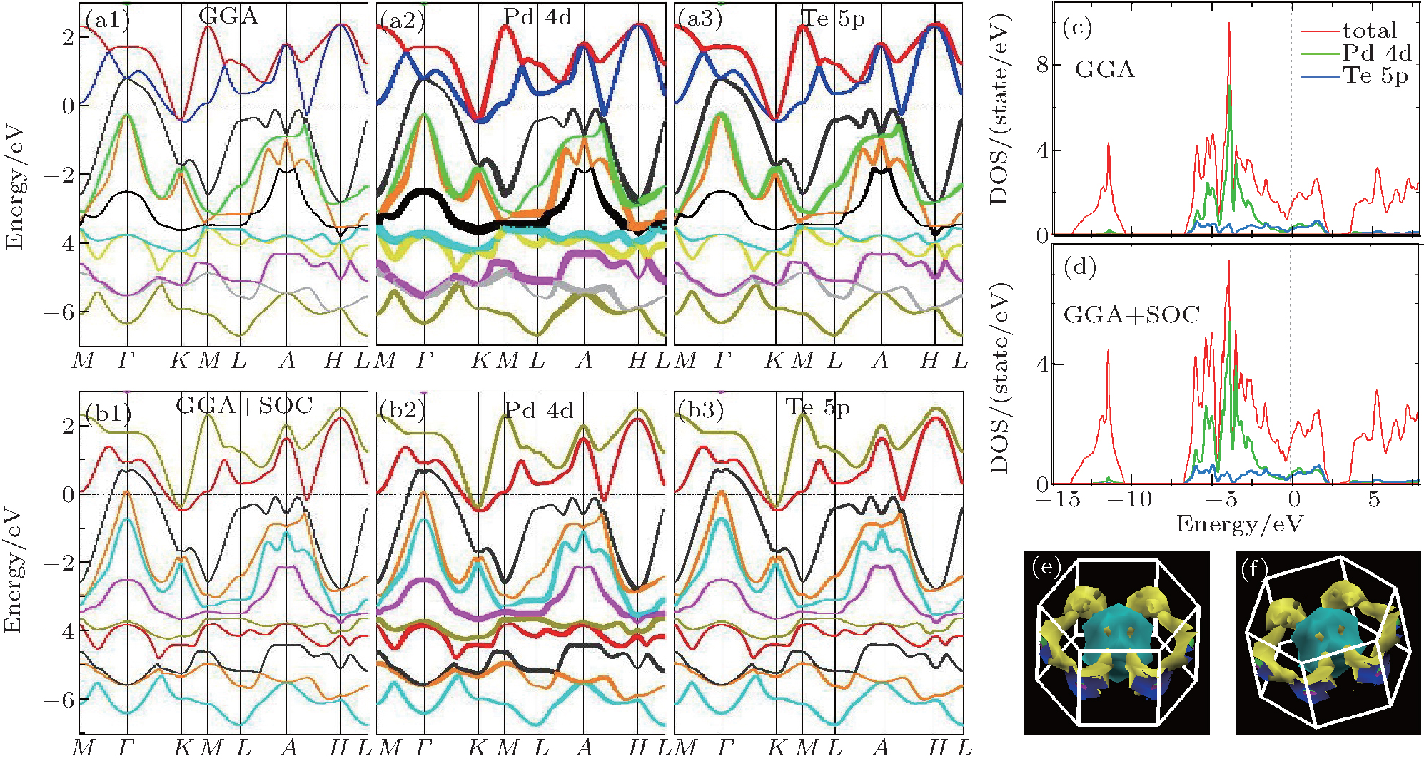
In order to understand the electronic structure of PdTe2 and have a direct comparison with the experiment, band structure calculations were carried out. Figure 6 shows the calculated band structure (Figs. 6(a) and 6(b)), the density of state (DOS) (Figs. 6(c) and 6(d)), and the three-dimensional Fermi surface (Figs. 6(e) and 6(f)), without and with considering the spin– orbit coupling. Our calculations overall agree with the previous report.[47] First, the electronic structure of PdTe2 shows strong three-dimensionality, as manifested from the different band structures on the MGK and LAH planes (Figs. 6(a) and 6(b)), and the three-dimensional Fermi surface topology seen in Figs. 6(e) and 6(f). The strong kz dependence of the constant energy contours and the band structure in Fig. 7 also support this picture. Second, the low-energy electronic states are mainly contributed by the Pd 4d states and Te 5p states, as seen from the calculated DOS in Figs. 6(c) and 6(d). At high binding energy above 2 eV, the Pd 4d state contributes most of the spectral weight, while around the Fermi level, the Te 5p state and Pd 4d state contribute nearly equally (Figs. 6(c) and 6(d)). It is interesting to note that the Fermi level EF is located near the valley of the overall density of states, indicating the existence of a low carrier density and that it is relatively easy to tune Tc.[45] The detailed spectral weight contributions of the Pd 4d and Te 5p orbitals are shown in Figs. 6(a2), 6(a3) and Figs. 6(b2), 6(b3) for each of the hybridized bands. Third, the spin– orbit coupling plays an important role in the electronic structure of PdTe2. While there are three bands that cross the Fermi level in the calculated band structure without considering the spin– orbit coupling (Fig. 6(a)), four band crossings are present in the calculated results with the spin– orbit coupling (Fig. 6(b)). The spin– orbit coupling also induces band splitting of several bands, as seen from Figs. 6(a) and 6(b). These results suggest that the spin– orbit coupling in PdTe2 has an obvious effect on the electronic structure. Our simulation on the spin– orbit coupling strength gives a value of ∼ 0.5 eV for PdTe2.
Figure 7 shows a comparison between our experimental results and the band structure calculations. Since the ARPES band structure measurement at a given photon energy provides only one line momentum cut in the three-dimensional momentum space, and the measured Fermi surface only represents a (curved) surface cut through the three-dimensional Fermi surface, it is important to locate kz of the ARPES measurements for the direct comparison. In the band structure calculations, we have calculated the Fermi surface and band structures along high symmetry momentum cuts at various kz. Figure 7(b) shows the calculated Fermi surface at four different kz (kz = 0, 1/3, 2/3, and 1) from Γ to A point with equal kz increment, the value of kz is in units of π /c. For kz = 0, there is an enclosed large polyhedron hole-like Fermi surface sheet surrounding the Γ point (Fig. 7(b1)), and two pairs of irregular pockets appear at the K points. The Fermi surface topology varies strongly with kz due to three-dimensionality of the electronic structure. For kz = 1, one sees only six small electron pockets in the first Brillouin zone. The corresponding band structure also shows a strong kz dependence as seen in Fig. 7(d).
Direct comparison between the measured and the calculated Fermi surfaces and band structures indicates that, our measured results fit closest to the kz = 1 case. The dominant feature, the observation of electron-like bright spots β (β ′ ) in the measured Fermi surface (Fig. 7(a)), shows the best fit to the calculated Fermi surface topology near kz = 1 (Fig. 7(b4)). This provides a way to estimate and check on the location of kz in our ARPES measurements using the helium lamp with a photon energy of 21.2 eV and the VUV laser with a photon energy of 6.994 eV. The momentum perpendicular to the sample surface during the photoemission process is given by  in units of Å − 1.[50] Considering kz to be 1 for 21.2-eV photon energy, the inner potential V0 can be roughly estimated to be 18.8 eV. This value is similar to that measured in other related transition metal dichalcogenides such as WTe2 with V0 = 14.5 eV[51] and IrTe2 with V0 = 14 eV.[50] This value can be further checked by our laser ARPES measurements, where kz = 3.88π /c is obtained with photon energy hν = 6.994 eV. This is close to the kz = 0 Γ MK plane, and indeed the observation of hole-like bands in the laser-ARPES measurements (Figs. 5(g)– 5(j)) is consistent with the calculated band structure at kz = 0 (Fig. 7(d1)). These results indicate that our selection of V0 and kz can capture the major observations of our measurements.
However, we note that, although there is a good correspondence on the major features, the deviations of our measurements from the band structure calculations are also obvious. The most notable one is the simultaneous observation of multiple Fermi surface sheets, like the α band near Γ , the two flaps (γ bands) around the K points, the δ bands extending out from the β bright spots, and other features in the second Brillouin zone. Some of them are difficult to find correspondence in the calculated Fermi surface at different kz planes. The simultaneous observation of multiple features may originate from poor kz momentum resolution which is not known at the point. Further detailed photon energy-dependent ARPES measurements may help clarify this issue.


 ]
]