


An analytical model of thermal mechanical stress induced by through silicon via*
[Dong Gang† , Shi Tao, Zhao Ying-Bo, Yang Yin-Tang]
, Shi Tao, Zhao Ying-Bo, Yang Yin-Tang]
|
|


†Corresponding author. E-mail: gdong@mail.xidian.edu.cn
*Project supported by the National Natural Science Foundation of China (Grant No. 61334003) and the Kunshan Innovation Institute of Xidian University.
We present an accurate through silicon via (TSV) thermal mechanical stress analytical model which is verified by using finite element method (FEM). The results show only a very small error. By using the proposed analytical model, we also study the impacts of the TSV radius size, the thickness, the material of Cu diffusion barrier, and liner on the stress. It is found that the liner can absorb the stress effectively induced by coefficient of thermal expansion mismatch. The stress decreases with the increase of liner thickness. Benzocyclobutene (BCB) as a liner material is better than SiO2. However, the Cu diffusion barrier has little effect on the stress. The stress with a smaller TSV has a smaller value. Based on the analytical model, we explore and validate the linear superposition principle of stress tensors and demonstrate the accuracy of this method against detailed FEM simulations. The analytic solutions of stress of two TSVs and three TSVs have high precision against the finite element result.
In the last several years, integrated circuits (ICs) have been enhanced in terms of performance, power consumption, etc, primarily by continuously scaling down the size of transistors. However, scaling down of semiconductor device will encounter physical limit. Therefore, some researchers proposed another direction to increase the device density by making ICs into three-dimensional (3D) spaces instead of traditional two-dimensional (2D) ICs. The 3D IC stacking has gained tremendous interest for IC integration in order to reduce wire length and footprint. In addition, several dies manufactured by different process technologies can also be integrated as one chip with 3D integration.[1– 5]
Through silicon via (TSV) is regarded as the best choice of the connection between wafer and wafer. By using TSVs in 3D integration, the system performance can be significantly improved and the manufacturing cost is reduced.[6– 9] However, there are still some challenges for this technology. In the TSV structure, between silicon substrate, dielectric material, Cu diffusion barrier, and filled metal, there are large coefficient of thermal expansion (CTE) differences. Due to the thermal expansion coefficient between different materials, the shrinkage degree of each material is also not the same as the same temperature load. The adhesion between each layer of material is close, which causes the same interface displacement between adjacent layers. Thus, the thermal stress is produced at the interface between two materials. For example, the CTE of copper is larger than the CTE of silicon dioxide. The CTE mismatch between copper and silicon causes inevitable stress on silicon and results in material failure.[10– 15] It will also affect the performance of devices which are around the TSV and reduce the life of the electronic device.[16, 17] Furthermore, the design parameters, such as the thickness and materials of Cu diffusion barrier and liner, have an impact on the mechanical reliability. Therefore, it is necessary to understand the stress distribution in silicon.
At present, most works on thermo-mechanical stress employ the finite element method (FEM) to characterize the stress.[18, 19] While the FEM can accurately analyze the stress of simple TSV placement, it encounters enormous difficulties when tackling a larger design due to its expensive memory consumption and high run time. However, analytical methods can overcome the difficulties of FEM. Analytical methods assume a TSV structure and some boundary conditions. With these conditions and physical relation, the analytical equations can be listed.[20] They are generally efficient and easy to be handled with acceptable error. Besides analytical methods, the linear superposition method has been used to complete the simulation of multiple TSVs condition within reasonable run time and memory usage.
In this paper, we present an accurate TSV thermal stress analytical model based on the Lamé stress solution, and verify its accuracy with the FEM. We also discuss the effects of Cu TSV radius, Cu barrier layer, and TSV liner on the stress. We analyze the stress of multiple TSV condition by using the linear superposition principle.
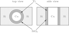
There are several TSV structures. The cylindrical TSV is easy to manufacture and became one of the most commonly used structures. The material of TSV also has different choices, such as Cu, W, and polycrystalline silicon. At present, Cu is the most commonly used interconnect materials in the integrated circuit process. In this paper, we use Cu as TSV material in order to be compatible with existing technology. In addition, the resistivity of Cu is minimum, which is also an advantage. Because the silicon has a certain conductive ability, it is necessary to add an insulation layer between Cu TSV and silicon substrate. SiO2 is a good insulating material. Cu can spread quickly in SiO2, so a barrier layer is need between the copper and SiO2. We select Ti as the barrier material. Based on the above analysis, the materials of each layer in the TSV structure from inside to outside, are Cu, Ti barrier layer, SiO2, and silicon substrate, respectively. The TSV baseline structure shown in Fig. 1 is used. In this paper, we adopt the NCSU 45 nm technology. The TSV radius, Cu diffusion barrier thickness, and liner thickness are 2.5 μ m, 50 nm, and 125 nm, respectively, which are based on the fabricated and published data.[21, 22]
 | Fig. 1. TSV baseline structure. |
For the analytical 2D radial stress model, known as Lamé stress solution, only the radial stress (σ rr) and hoop stress (σ θ θ ) are presented in Ref. [20]. The area of silicon substrate is much larger than that of TSV, and this paper is to characterize the interactive stress in device layer, so the strain constraint in the silicon substrate is determined by the silicon substrate and can be neglected in the z axis direction; namely, the stress in the z axis direction is zero.[23] The stress in silicon substrate region can be expressed as follows:


where σ Si is the stress in the silicon substrate, E is the Young’ s modulus, Δ α is the mismatch in CTE, Δ T is the differential thermal load, r is the distance from the TSV center, and DTSV is the TSV diameter.
Even though this closed-form formula is easy to handle, this solution is only applicable to the structure with TSV and substrate. It does not contain Cu diffusion barrier thickness and liner. The parameters such as the thickness and materials of Cu diffusion barrier and liner have impacts on the mechanical reliability. In our study, we consider the impacts of Cu diffusion barrier thickness and liner on the stress.
Based on the axisymmetric structure of TSV, using plane stress theory and under force equilibrium conditions, the geometric equations and the axisymmetric equilibrium equation can be obtained as


where 


Because the stress is caused by temperature change, the physical equations for temperature changes are
 |
 | /tr>
 |
where 
In the silicon substrate, the radial stress and hoop stress are equal in magnitude and opposite in direction.[20] Substituting 
 |
 |
 |
In order to guarantee that the TSV structure has the same height as the silicon substrate in the z axis direction, we set the TSV strain to be the strain in the silicon substrate, namely, 
 |
 |
In combination with the geometric equations and the axisymmetric equilibrium equation, the following expressions can be obtained:


In Eqs. (9)– (11), C1 and C2 are the constants determined by the boundary conditions.
With the boundary conditions, the displacement at the center of the TSV is zero, and the stress is zero at infinity. The following equations can be obtained for the continuity of displacements and stresses at interfaces:


where rCu, rTi, and rSiO2 denote the radius of Cu, the outer radius of Ti, and the outer radius of SiO2, respectively.
Using the above equations, all of the constants can be determined, and then the analytical model of the TSV stress is obtained.
The FEA simulations are used to verify the accuracy of the analytical model. Material properties are shown in Table 1, [22] and assumed to be linearly elastic. The thermal load Δ T = − 250 ° C. That is, we assume that the TSV structure is annealed at 275 ° C and cooled down to 25 ° C to mimic the manufacturing process. At the same time, it is assumed that the stress becomes negligible in silicon substrate away from the via. The boundary conditions for the continuity of displacements and stresses at interfaces are used in the simulation.
| Table 1. Material properties. |
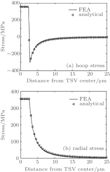
Figure 2 shows a comparison of analytical model and finite element simulation. The plus sign stands for the tensile stress and the minus sign the compressive stress. Figure 2(a) is the hoop stress contrast. Figure 2(b) is the radial stress contrast. It can be seen from the figure that the error between analytical model and the finite element model is less than 2% and can be neglected. The accuracy of the analytical model is verified. The distances of the stress dropping every 50 MP from 300 MP to 50 MP are 0.26, 0.36, 0.52, 0.88, and 1.98 μ m, respectively. The stress in silicon drops increasingly slowly with the increase in distance from the TSV boundary.
 | Fig. 2. Comparison between analytical model and FEA simulation of a single TSV. (a) Hoop stress; (b) radial stress. |
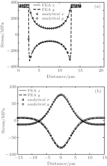
Figure 3 shows the stress contour map of the FEA simulation and the analytical model of a single TSV. Through comparison, we can see that the stress distribution is the same. It can also be found that σ x is equal to the radial stress on the x axis and σ y is equal to the hoop stress. The situation on the y axis is just the opposite. σ x is equal to the hoop stress, and σ y is equal to the radial stress.
 | Fig. 3. Stress contour map of (a), (b) the FEA simulation and (c), (d) the analytical model of a single TSV. |
The Cu TSV size, the thickness of Cu diffusion barrier, and the liner have effects on stress. Figure 4(a) shows the radial stress contrast with different thickness of Ti and SiO2. It can be seen that when the thickness of SiO2 is 125 nm and 500 nm, respectively, the stress increases 0.43 MP and 0.58 MP with the thickness of Ti increasing from 50 nm to 100 nm, respectively. When the thicknesses of Ti are 50 nm and 100 nm, respectively, the stress increases 27.49 MP and 27.34 MP with the thickness of SiO2 increasing from 50 nm to 100 nm, respectively. The stress is reduced with increasing SiO2 but is almost the same with increasing Ti. This is mainly because the Young’ s modulus of Ti is between Cu and Si, and its thickness is small. Its influence can be neglected. However, the Young’ s modulus of SiO2 is less than that of Cu and Si, and it is thicker. Therefore, SiO2 can absorb the stress, and act as a stress buffer layer.
 | Fig. 4. (a) Impact of the thickness of Cu diffusion barrier and liner. (b) Impact of the materials of TSV liner. (c) Impact of the materials of Cu diffusion barrier. (d) Impact of the size of TSV radius. |
The materials of the TSV liner can also affect stress. We employ benzocyclobutene (BCB), a polymer dielectric material, as an alternative TSV liner material. Figure 4(b) shows the impact of liner material and its thickness on radial stress. It can be found that when the thickness of the insulation layer thickness is 125 nm, and the insulation materials change from SiO2 to BCB, the stress reduces by 110.56 MP. When the thickness of the insulation layer thickness is 500 nm, the stress reduces by 169.99 MP. The stress reduces by 86.92 MP as the thickness of BCB increases from 125 to 500 nm. This is because the Young’ s modulus of BCB is much lower than Cu, Si, and SiO2, the BCB liner can absorb the stress more effectively due to the CTE mismatch.
However, the effect of Cu diffusion barrier material on stress is much smaller than TSV liner, as shown in Fig. 4(c). When the thickness of the barrier layer is 50 nm, and the insulation materials change from Ti to Ta, and the stress increases by 3.87 MP. When the thickness of the insulation layer thickness is 100 nm, the stress increases by 2.91 MP. The CTE of both Ti and Ta is between Cu and Si. Hence, it is unlikely to induce additional stress around TSV. However, Young’ s modulus of Ta is higher than that of Ti. Its stress is a little higher.
Figure 4(d) shows the impact of the size of TSV radius. We can find that with the decrease in the TSV radius size, the stress in TSV has a decline. The smaller TSV is, the more the stress drops. The stress in the silicon substrate with a smaller TSV declines more quickly with the increase in the distance from TSV boundary. That is, the stress with a smaller TSV has a smaller value with the same distance from the TSV boundary. The distances of the stress dropping from 300 MP to 50 MP are 0.26, 0.53, and 0.79 μ m, respectively.
A useful principle in the analysis of linearly elastic structures is that of superposition. The principle states that if the displacements at all points in an elastic body are proportional to the corresponding forces, that is the body is linearly elastic. The effects, i.e., stress and displacement, of a number of forces acting simultaneously on such a body are the sum of the effects of the forces applied separately. We apply this principle to compute the stress at a point by adding the individual stress tensors at that point caused by each TSV, as follows:

where S is the total stress at the point under consideration, and Si is the individual stress tensor at this point due to the ith TSV.
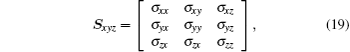
To evaluate a stress tensor at a point affected by multiple TSVs, a conversion of a stress tensor to a Cartesian coordinate system is required. Let the stress tensor in Cartesian and cylindrical coordinate system be Sxyz and Srθ z, respectively,

The transform matrix Q has the form of

where θ is the angle between the X axis and a line from the TSV center to the simulation point. A stress tensor in a cylindrical coordinate system can be converted to a Cartesian coordinate system using conversion matrices: Sxyz = QSrθ zQT.
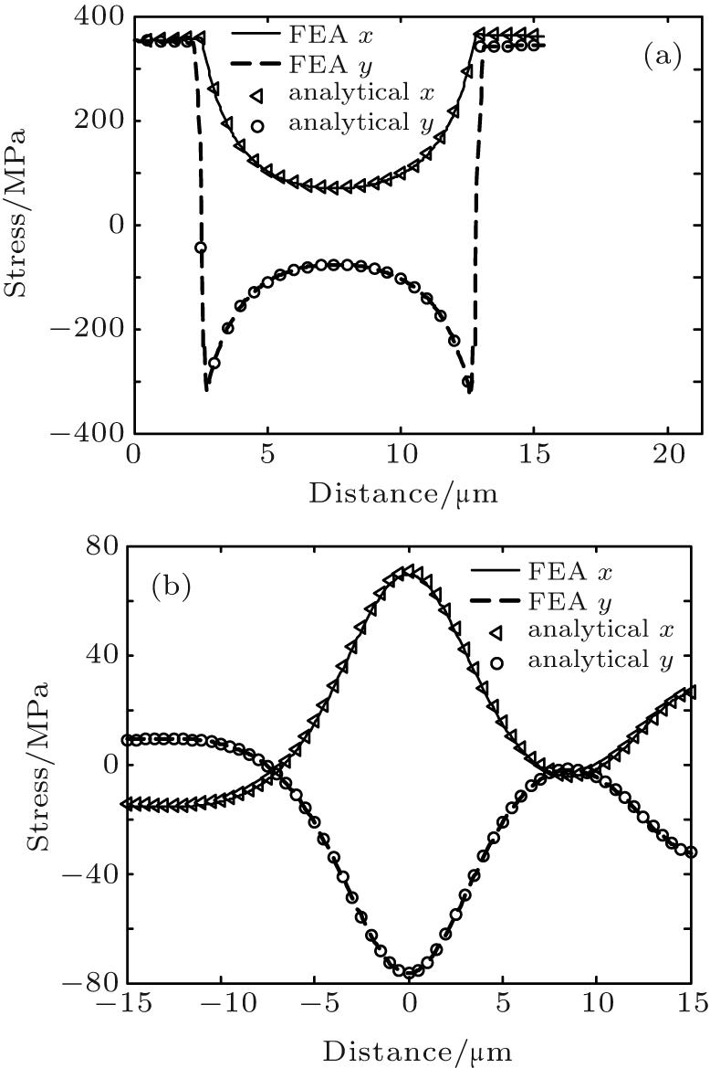
The spacing between two TSVs is 10 μ m, as shown in Fig. 5. The comparison results between the linear superposition and the FEA simulation of three TSV rectangular arrangements are shown in Figs. 6(a) and 6(b). Figure 6(a) shows the stress along the straight line between the two TSVs, and the origin of coordinates is one of the TSV center. Figure 6(b) shows the stress along the perpendicular bisector of the straight line between the two TSVs, and the origin of coordinates is the intersection of the two lines. The plus and minus of distance, respectively, mean the stress point on the top of or on the bottom of the origin point. The x represents the x direction stress, and the y represents the y direction stress. It can be seen from the figure that the results of the linear superposition method and the FEA simulation are almost identical, and the error is less than 2%, which demonstrates the accuracy of this method and of the analytical model.
 | Fig. 5. Two TSVs. |
 | Fig. 6. Comparison between FEA simulation and linear superposition method with two TSVs. (a) Stress along the straight line between two TSVs; (b) stress along the perpendicular bisector of the straight line between two TSVs. |
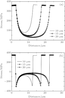
Figure 7 shows the comparison of the stress with two TSVs with different spacing. The stress is along the straight line between the two TSVs, and the origin of coordinates is one of the TSV centers. It can be seen that the stress with larger spacing reduces more quickly in the Si substrate. The distances of the stress dropping to 100 MP are 5.46, 5.03, and 4.92 μ m with the spacing being 10 μ m, 15 μ m, and 20 μ m, respectively. The area with smaller stress is larger, which means that more devices can be placed.
 | Fig. 7. Comparison of the stress with two TSVs with different spacings. (a) Radial stress; (b) hoop stress. |
For three TSVs analysis, there are two kinds of circumstances. (i) Three TSVs are arranged at right angles, with the spacing between the two TSVs at the square edge being 10 μ m, [11] as shown in Fig. 8(a). (ii) Three TSVs are in a row, with the spacing between the two TSVs being 10 μ m, [12] as shown in Fig. 8(b).
 | Fig. 8. Arrangement of three TSVs. (a) At right angle; (b) in a row. |
The comparison of results between the linear superposition and the FEA simulation of three TSVs rectangular arrangement is shown in Fig. 9. Figure 9(a) shows the stress along the straight line between the bottom two TSVs, and the origin of coordinates is the center of the TSV on the left. Figure 9(b) shows the stress along the perpendicular bisector of the straight line between the bottom two TSVs, and the origin of coordinates is the intersection of the two lines. Figure 10 shows the comparison results of three TSVs linear arrangement. Figure 10(a) shows the stress along the straight line between the three TSVs, and the origin of coordinates is the center of the TSV on the left. Figure 10(b) shows the stress along the perpendicular bisector of the straight line between the left two TSVs, and the origin of coordinates is the intersection of the two lines. x represents the x axis stress, and y represents the y axis stress. Through comparison, it can be seen that the linear superposition and the FEA simulation match very well. The error is less than 2% and can be practically negligible.
The analytical model is verified by the above simulations, which also prove the applicability of the linear superposition. The analytical model can be used to discuss the stress with more TSVs. It uses less time and computing resources compared with the FEA simulation.
 | Fig. 9. Comparison between the FEA simulation and the linear superposition method with three TSVs rectangular arrangement. (a) Stress along the straight line between the bottom two TSVs; (b) stress along the perpendicular bisector of the straight line between the bottom two TSVs. |
 | Fig. 10. Comparison between the FEA simulation and the linear superposition method with three TSVs linear arrangement. (a) Stress along the straight line between three TSVs; (b) stress along the perpendicular bisector of the straight line between the left two TSVs. |
An analytical model of thermal stress is given in this paper. The comparison between this model and detailed FEM simulations shows that the analytical model has high accuracy. The impacts of the Cu TSV size, the thickness, and material of Cu diffusion barrier and liner on stress have been studied. It is found that the liner can absorb the stress effectively induced by CTE mismatch, and BCB as a material of liner is better than SiO2. The stress decreases with the increase of liner thickness. However, the Cu diffusion barrier has little effect on the stress. The stress with a smaller TSV has a smaller value. On the basis of the analytical model, the principle of linear superposition is validated against the FEA simulation. The analytical solutions of the stress of two TSVs and three TSVs prove the applicability of the linear superposition, and demonstrate that the analytical model can be used for multiple TSVs stress analysis.
| 1 |
|
| 2 |
|
| 3 |
|
| 4 |
|
| 5 |
|
| 6 |
|
| 7 |
|
| 8 |
|
| 9 |
|
| 10 |
|
| 11 |
|
| 12 |
|
| 13 |
|
| 14 |
|
| 15 |
|
| 16 |
|
| 17 |
|
| 18 |
|
| 19 |
|
| 20 |
|
| 21 |
|
| 22 |
|
| 23 |
|