Simulation and experimental study of high power microwave damage effect on AlGaAs/InGaAs pseudomorphic high electron mobility transistor*
Key Laboratory of Ministry of Education for Wide Band-Gap Semiconductor Materials and Devices, School of Microelectronics, Xidian University, Xi’an 710071, China
†Corresponding author. E-mail: xhyu@stu.xidian.edu.cn
*Project supported by the National Basic Research Program of China (Grant No. 2014CB339900) and the National Natural Science Foundation of China (Grant No. 60776034).
1. IntroductionNowadays the pseudomorphic high electron mobility transistor (pHEMT) has established itself as a high performance device for wireless handsets and radio frequency (RF) communication systems. Because of its inherent merits such as low noise, low on-resistance, high power, and high frequency operation, AlGaAs/InGaAs pHEMT has been demonstrated to be able to fulfill the high requirements for the fourth generation wireless communications technology.[1]
Due to the harsh demands of the commercial and especially military applications, the reliability of the AlGaAs/InGaAs pHEMT is naturally a key matter that attention must be paid to. The degradation effect of pHEMT devices, [2– 5] such as hot carrier degradation, has been studied. The pHEMT may suffer hot carrier injection due to a strong electric field in the drain region.[4, 5] Hot carriers degrade the transistor in DC and RF performances.[5] However, for the intentional electromagnetic interference (IEMI), the reliability problem of pHEMT is usually the physical damage effect, rather than only degradation. The HPM can couple into the electronic systems through either the front-door path or the back-door path, and then cause temporary or permanent damage to the device inside integrated circuits (ICs).[6] The IEMI-induced damage effects on diode limiters, bipolar junction transistors (BJTs), and metal– oxide– semiconductor field-effect transistors (MOSFETs) have been reported in recent years. The electro– thermal characteristics of the second breakdown in diodes and the motion of current filaments in avalanching PIN diodes were respectively analyzed in Refs. [7] and [8]. The electromagnetic pulse (EMP) damage mechanism and the pulse properties-dependent damage susceptibility of Si-based BJTs are investigated in Refs. [9]– [12]. Likewise, the latch-up effect in complementary metal– oxide semiconductor (CMOS) inverter induced by HPM was analyzed in Ref. [13]. Unfortunately few conclusions have been reported for the HPM damage to pHEMT, and the damage mechanism and pulse properties-dependent damage susceptibility trends have remained unclear.
One of the purposes of this work is to analyze the HPM damage mechanism of pHEMT from the aspect of physical behavior. By simulation, the distributions of current density, electric field strength, and lattice temperature within the device are plotted to facilitate understanding the mechanism. Another contribution of this work is to determine whether the HPM damage to pHEMT has a pulse-width dependence similar to the damage to other semiconductor devices. Furthermore, the accurate empirical formulas are proposed to estimate the HPM damage susceptibility. Finally, the simulated results will be verified experimentally.
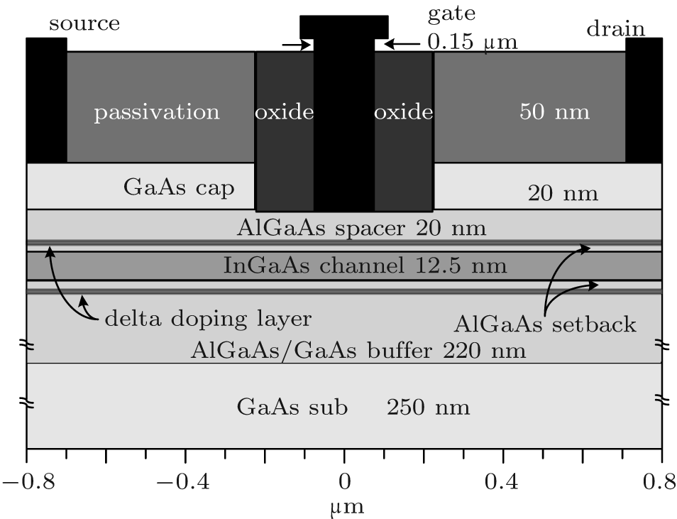
2. Device structure and simulation details2.1. Device structureIn this paper the double δ -doping AlGaAs/InGaAs pHEMT is studied. Figure 1 shows its basic structure as simulated in TCAD. The structure is comprised of GaAs substrate, AlGaAs/GaAs buffer, AlGaAs setback layer, InGaAs channel, AlGaAs setback layer, AlGaAs spacer layer, and GaAs cap layer. There also exist two δ -doping layers near each setback layer. Furthermore, the device surface is passivated with Si3N4 and SiO2. The gate length is 0.15 μ m and the width is 280 μ m. Inside this structure, double heterojunctions exist among the AlGaAs/InGaAs/AlGaAs layers. Then the double heterojunctions form a quantum well structure, which makes the density of electrons for the two-dimensional electron gas (2DEG) even higher.
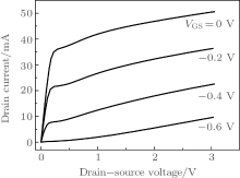
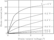
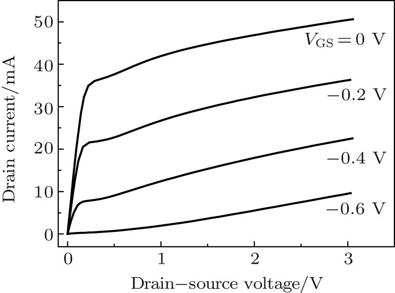
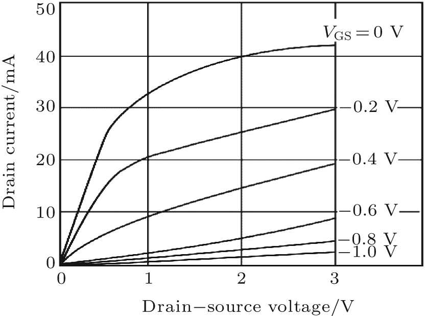
2.2. Simulation detailsIn order to accurately depict the damage effect and the microscopic behavior within the device, the device simulation based on TCAD is adopted in this paper and a large number of physical models are required. During the action of the HPM, a significant rise in temperature requires the thermodynamic model accounting for self-heating effect. The hydrodynamic model accounting for the energy transport of carriers and other models such as the avalanche model accounting for impact ionization with self-heating are all taken into account in the simulation to improve the calculation precision. The description and physical equation for each of these models are available in Ref. [14]. Based on the simulation model, the DC characteristics of the pHEMT, i.e., a family of curves for IDS versus VDS for increasing VGS, are acquired and shown in Fig. 2. Besides, the threshold voltage of the pHEMT is about − 0.95 V.
Generally the HPM radiation energy couples into interior electronics of a system through either the front-door path or the back-door path.[15] In this paper the HPM is assumed to be a sinusoidal wave without attenuation, and is injected into the gate terminal of pHEMT to simulate the process that the HPM energy couples into the input port of the pHEMT low noise amplifier (LNA) through the front-door path.[16] In addition, the boundary condition with 0.1 cm2· K/W surface thermal resistance on the bottom side and the constant ambient temperature (300 K) for the device are adopted in the simulation.
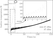
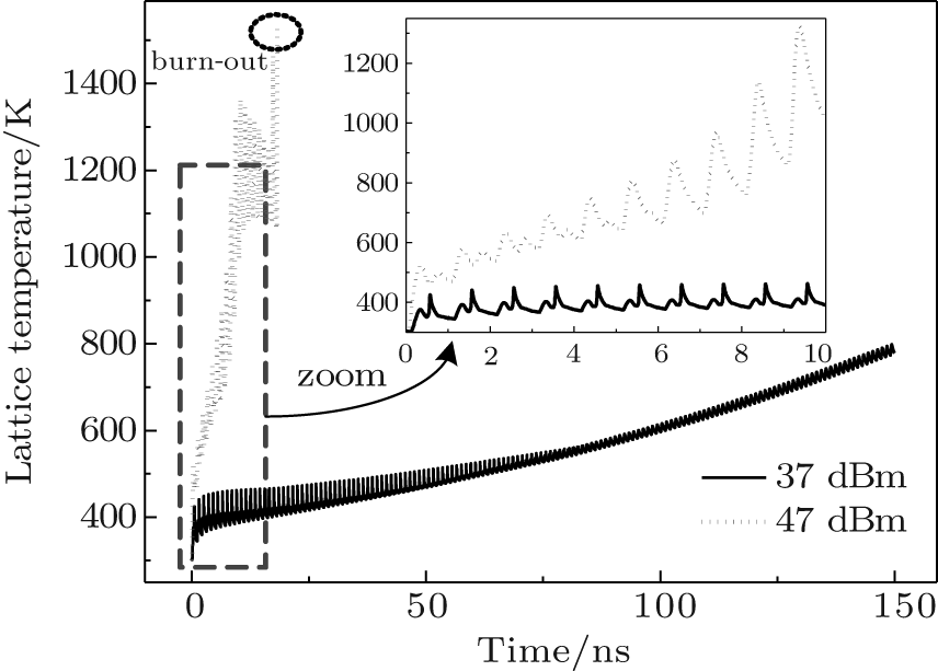
3. Simulated results and discussion3.1. HPM damage effect and mechanismAs presented previously, HPMs with increasing the power level, fixing frequency at 1 GHz and pulse repletion frequency (PRF) at 0, are injected into the gate terminal. Meanwhile the drain voltage is biased at 2 V and the source is grounded. Figure 3 shows the variations of the maximum temperature inside the device with time. When the power level of injected HPM equals 37 dBm, the variation in temperature with time is slight. Though the temperature behaves as periodic “ increasing– decreasing– increasing” oscillation and the whole trend continuously increases with time, the maximum temperature does not exceed 800 K till 150 ns. Nevertheless, as the power level is elevated to 47 dBm, the temperature sharply rises and quickly reaches 1511 K (the GaAs melting point) at 18 ns. So it can be inferred that device burn-out may occur and it is the key failure mode of pHEMT under HPM action.
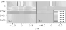
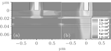
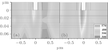
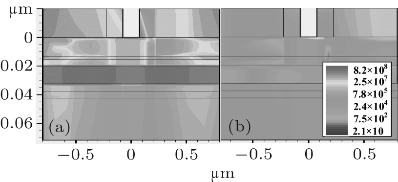
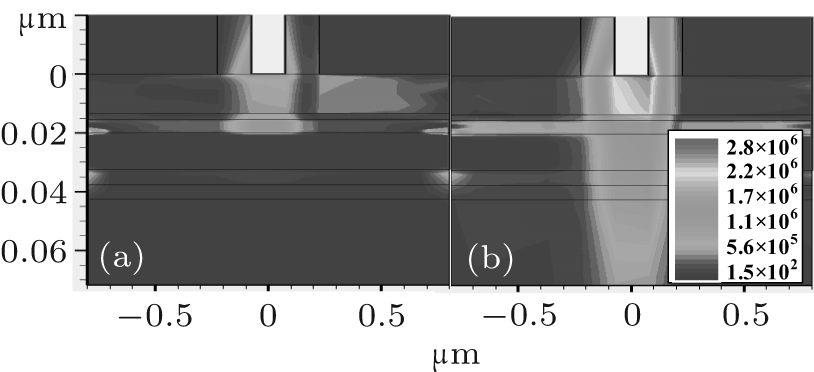
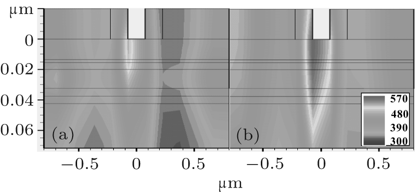
According to the inset in Fig. 3, the temperature first increases and then decreases in each cycle. Here the situation that HPM with a power of 47 dBm is injected into pHEMT is taken for example. Figures 4– 6 respectively show the distributions of current density, electric field strength, and temperature within the device at 1.2 ns and 1.8 ns. It can be obviously seen from Fig. 4(a) that a current path emerges beneath the gate and connects the gate with the InGaAs channel during the positive half cycle of HPM. Besides, the current path is closer to the source side than the drain. That is because the drain voltage is biased at 2 V so that the gate/source voltage is larger than the gate/drain voltage. During the negative half cycle, the current density is extremely low because the Schottky junction is reverse-biased (see Fig. 4(b)). In contradiction to the current density, the electric field strength beneath the gate at 1.8 ns is much larger than that at 1.2 ns (Fig. 5). This is due to the fact that the gate/source and gate/drain voltages mostly drop on the reverse-biased Schottky junction during the negative cycle. Actually even during the positive cycle, the electric field strength beneath the gate is still as high as a level of 105 V/cm∼ 106 V/cm (see Fig. 5(a)), and as is well known, the heat generated in the transistor can be expressed as Q = J · E, determined by both the current density J and the electric field strength E. Hence a large amount of heat is assumed to be generated during the positive half cycle.
Figure 6 verifies this opinion. From Fig. 6(a) to Fig. 6(b), the hotspot spreads several times in area but is still located beneath the gate near the source side. So it can be concluded that the emerging current path and strong electric field beneath the gate during the positive cycle dominantly contribute to device burn-out.
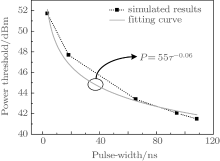
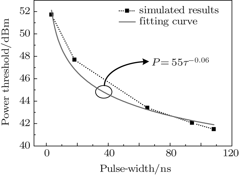
3.2. HPM pulse-width-dependent damage effectIn order to investigate the pulse-width dependence of the HPM damage, the sinusoidal voltage signals with a frequency of 1.3 GHz and ascending voltage amplitude are respectively injected into the gate terminal. Similarly, the drain voltage is biased at 2 V and the source is grounded. The HPM pulse-width is calculated by the time duration of the injected signal before the device is burned out, and the damage power threshold P is the average power absorbed by the device in the injection process. Then the dependence of damage power threshold P on pulse-width τ is acquired and illustrated in Fig. 7. It indicates that the HPM damage power threshold decreases with the increase of pulse-width and the dependence is evidently nonlinear. By the curve fitting method, the empirical formula describing the dependence can be obtained as follows:

where P is in dBm and τ in ns. The formula is expected to be capable of quickly estimating the HPM damage power threshold regarding the influence of pulse-width.
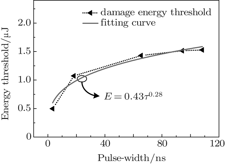
Empirical formulas regarding the DC pulse power required to cause degradation or failure in semiconductor junction devices for the nanosecond pulse duration (1 ns ∼ 100 ns) were developed by Wunsch and Bell, [17] and Tasca, [18] indicating that the absorbed energy causing degradation or failure does not depend on the pulse-width. However, the experimental study by Brown[19] on threshold levels for damage to transistors showed that the transistor absorbed energy exhibits a different response to DC nanosecond pulses (3 ns∼ 55 ns) by the direct injection approach, and concluded that no formula can yield accurate threshold levels for all device types. As to pHEMT, few reports focus on the energy characteristics. Hence the empirical formula, describing the energy characteristic and applied only to pHEMT, should be determined. In this paper, it is shown that the pHEMT absorbed energy causing damage cannot be absolutely constant but slowly increases with the increase of pulse-width as shown in Fig. 8. Similarly, the empirical formula describing the dependence of the damage energy threshold E on pulse-width τ is obtained as follows:

where E is in μ J and τ in ns. The particular damage energy characteristic is due to the fact that the energy absorbed at the damage position will be dissipated towards the surrounding regions with time going by. So the dissipated heat relieves the acute increasing of temperature at the hotspot for longer pulse-width. It can be determined that HPM with longer pulse-width requires lower power density but more energy to cause the damage to pHEMT.
4. Experimental studyIn order to validate previous conclusions, the HPM injection experiments on the LNAs consisting of our pHEMT samples are carried out. There are four ceramic packaged pHEMT samples in this work, respectively numbered 1#– 4#. The sample is utilized as the first stage transistor of a dual-stage LNA. Our pHEMT sample has the similar structure and DC characteristics as the simulation model does. It has the same gate length of 0.15 μ m and width of 280 μ m, and its output DC characteristic is depicted in Fig. 9. Compared with Fig. 2, the saturation drain current of the sample is just a little lower than that of the simulation model, and the two characteristics are very close to each other on the whole.
The injected HPM signals are continuous waves with high density power, which are generated by a Synthesized Sweeper (HP 83630A), modulated by a Pulse Generator (HP 81130A) and then amplified in power by a power amplifier. Then HPMs with frequency 1.3 GHz, pulse-width 60 μ s, 4 μ s, 20 ns, and 1 ns and incremental power density are respectively injected into the input port of LNAs. Similarly, the drain bias is 2 V and the source terminal is grounded. Differing from simulation, the maximum temperature within the device is difficult to be extracted in actual experiments, so that the noise figure of LNA deteriorating to 20 dB serves as the damage criteria.[20] The stepping technique is adopted in the power injection experiments, and the stepping interval is 1 dBm. The experimental results are listed in Table 1.
Table 1.
Table 1.
 Table 1. The sample number and failure condition.| Sample number | LNA number | Pulse-width/ns | Damage threshold/dBm |
|---|
| 1# | No.1 | 6 × 10⁴ | 31 | | 2# | No.2 | 4 × 10³ | 32 | | 3# | No.3 | 20 | 41 | | 4# | No.4 | 1 | 52 |
| Table 1. The sample number and failure condition. |
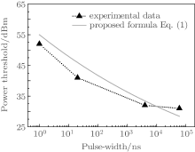
Table 1 demonstrates that the damage power threshold decreases with incremental pulse-width, verifying the trend obtained by simulation. Furthermore, by contrast, the empirical formula Eq. (1) proposed in this paper is almost exactly in accordance with the experimental data, as shown in Fig. 10. Even the pulse-width increases to the microsecond and millisecond level, the estimation error still sustains very little. So it can be determined that the proposed empirical formula Eq. (1) no doubt applies to actual applications in quickly and accurately estimating the HPM damage power threshold of pHEMT. At the same time, the special pulse-width-dependent damage energy characteristic concluded in this paper can also be verified.
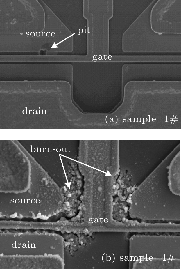
To further learn about the HPM damage effect, scanning electron microscopy (SEM) is used to observe the interior of the damaged sample. Observation indicates that for all the damaged samples, one or more pits emerge between the source and gate contact (see Fig. 11(a)). The pits of this kind are in fact formed by the process that high current density and strong electric field cause temperature to continuously increase and then the device is partially melted due to overheating, namely burn-out. This verifies the previous analysis in this paper that the burn-out caused by the emerging current path and strong electric field beneath the gate is responsible for the HPM damage. Figure 11(b) shows the burn-out feature of sample 4# damaged by HPM with a width of 1 ns. It can be obviously found that not only the semiconductor material beneath the gate but also the gate metal is melted severely. This is due to the fact that the HPM with a shorter pulse-width requires a much higher voltage amplitude to cause damage to pHEMT, so that the injection current is too large for the gate metal to survive the burn-out. Even then, it can be clearly seen that the source side is burned out more severely than the drain side, excluding the influence of melted gate metal. Hence it demonstrates that the location beneath the gate near the source side is most susceptible to burn-out, which is in accordance with the simulated results.
5. ConclusionsIn this paper the HPM damage effect on 0.15-μ m gate AlGaAs/InGaAs pHEMT is studied by simulation based on TCAD and experiments. Simulated results suggest that the HPM damage to the pHEMT is mainly due to the device burn-out caused by the emerging current path and strong electric field beneath the gate near the source side. Besides, the damage to pHEMT shows the pulse-width dependence that the damage power threshold decreases but the energy threshold slightly increases with the increase of pulse-width. Then the HPM pulse-width damage effect is verified by experimental results. The experimental verification demonstrates that the proposed empirical formula P = 55τ − 0.06 is capable of quickly and accurately estimating the HPM pulse-width-dependent damage power threshold of pHEMT. The special energy characteristic is also verified, indicating that HPM with shorter pulse-width requires higher power density but less energy to cause the damage to the pHEMT. Finally the interior observation of damaged samples by SEM illustrates that the failure mechanism of the HPM damage to the pHEMT is indeed device burn-out and the location beneath the gate near the source side is most susceptible to burn-out, which is in accordance with the simulated results.


 , Chai Chang-Chun, Liu Yang, Yang Yin-Tang, Xi Xiao-Wen]