†Corresponding author. E-mail: yuanjiren@ncu.edu.cn
‡Corresponding author. E-mail: lzhou@ncu.edu.cn
*Project supported by the National Natural Science Foundation of China (Grant Nos. 61464007, 61306084, and 51361022), the Postdoctoral Science Foundation of Jiangxi Province, China (Grant No. 2014KY32), and the Natural Science Foundation of Jiangxi Province, China (Grant No. 20122BAB202002).
The near-infrared responsivity of a silicon photodetector employing the impurity photovoltaic (IPV) effect is investigated with a numerical method. The improvement of the responsivity can reach 0.358 A/W at a wavelength of about 1200 nm, and its corresponding quantum efficiency is 41.1%. The origin of the enhanced responsivity is attributed to the absorption of sub-bandgap photons, which results in the carrier transition from the impurity energy level to the conduction band. The results indicate that the IPV effect may provide a general approach to enhancing the responsivity of photodetectors.
Photodetectors are optoelectronic devices for detecting optical signals and converting them into electrical signals, and they possess many applications, such as image sensing, chemical sensing, communications, environmental monitoring, and remote control.[1– 5] In order to better implement these applications, higher performance photodetectors are always required. Responsivity is one of the most important parameters that determine the property of a photodetector, and it is defined as the light signal generated current in a photodetector divided by incident optical power. Thus, it will be of great significance if a general approach to enhancing the responsivity of a photodetector can be found.
We found that a potential approach to enhancing the responsivity is to employ the impurity photovoltaic (IPV) effect. The mechanism of the IPV effect is to introduce an impurity energy level within the bandgap so that some photons with energies less than the bandgap can be absorbed by the semiconductor device.[6– 8] This action would increase the current output and improve the responsivity of a photodetector. Mohammed et al.[9] used the MATLAB program to calculate the photogenerated current in a PN silicon photodetector, enhanced by the impurity photovoltaic effect. Their results indicated that using the impurity photovoltaic effect can improve the photogenerated current of photodetectors and widen the operating wavelength range toward the near infrared region.
In the present work, we select silicon-based photodetectors to theoretically investigate the responsivity by employing the IPV effect. The dependences of responsivity on the device thickness, the IPV impurity concentration, and the internal reflection coefficient are reported and discussed.
The schematic plot of the IPV effect is shown in Fig. 1. It can be seen that the model includes the conventional Shockley– Read– Hall (SRH) mechanism (right side) and two impurity optical transitions (on the left-hand side). A photon with energy hν 1 excites an electron from the valence band to an impurity level, and the second photon of energy hν 2 pumps the electron from there to the conduction band. So, two photons with energies less than the bandgap can generate an electron– hole pair by a two-step transition. The SRH model can be modified due to the addition of the IPV effect. The net recombination rate U via impurity is given by[6]

with


where n and p are the electron and hole concentrations, n1 and p1 the electron and hole concentrations when the Fermi level coincides with the impurity level, NC and NV the effective densities of states in conduction and valence bands, EC and EV the conduction and valence band edges, Et is the impurity energy level, τ n0 and τ p0 are the lifetimes for electrons and holes, gnt and gpt the optical emission rates from the impurity for electrons and holes, Nt is the impurity concentration, υ th the carrier thermal velocity (107 cm/s), 


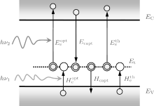 | Fig. 1. Schematic of the IPV effect, showing that two sub-bandgap photons (hν 1 and hν 2) create an electron-hole pair via impurity level Et |
The photon flux ϕ ph (x, λ ) at depth x from the incident surface for the wavelength λ is given by the following expression:

with


where ϕ ext is the external incident photon flux, L the total thickness of the cell, Rf and Rb are the internal reflection coefficients at the front and back surface of the cell, α e− h is the band-to-band absorption coefficient, α n and α p are the impurity absorption coefficients for electron and hole photoemission from the IPV impurity, α fc is the absorption coefficient for free-carrier absorption, and ft the occupation probability of impurity level.
In the SCAPS simulation program, [10, 11] the silicon photodetector considered in this study is a p+ − n− n+ structure. For the p+ emitter layer, the doping concentration NA and the thickness are set to be 1018 cm− 3 and 2 μ m, respectively; for the n-base layer, the carrier concentration ND is set to be 1017 cm− 3, and the thickness is set to be 100 μ m; for the n+ layer, the carrier concentration ND and the thickness are 1018 cm− 3 and 5 μ m, respectively. The indium element is selected as the IPV impurity. The indium energy level in silicon is at 0.157 eV above the valence band edge.[12] This level location is a good choice because the impurity will act as an effective recombination center if the impurity level location is too close to the middle of the bandgap, and the IPV effect of the sub-bandgap photons will be negligible if the level location is too close to the valence band edge or the conduction band edge. The electron and hole thermal capture cross-sections for indium impurity are set to be 2× 10− 22cm2 and 8× 10− 15cm2, respectively.[6] The basic parameters used for the silicon photodetector at 300 K are listed in Table 1.[12, 13] The electron and hole photoemission cross-sections of the IPV impurities are calculated according to the model of Lucovsky.[14]

| Table 1. Basic parameters for the silicon photodetector used in this study (at 300 K). |
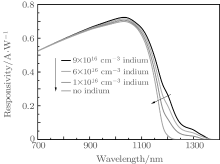
Figure 2 shows the variations of responsivity with incident wavelength for different indium concentrations. It is found that the responsivities of the photodetectors doped with the IPV indium impurity are greater than those of the photodetectors without indium impurity when the wavelength is longer than about 900 nm. The improvement of responsivity increases with increasing the indium concentration. When the wavelength is 1000 nm, the responsivities of the photodetectors doped with 9× 10− 16, 6× 10− 16, and 1× 10− 16 cm− 3 indium impurities are 0.714, 0.706, and 0.698 A/W, respectively. If no indium is introduced, the responsivity is 0.691 A/W. When the wavelength is 1160 nm, their responsivities are 0.440, 0.394, and 0.339 A/W, respectively, for the photodetectors doped with 9× 10− 16, 6× 10− 16, and 1× 10− 16cm− 3 indium impurities. While the responsivity without IPV indium is only 0.293 A/W. Moreover, the responsivities of the photodetectors have some extensions to near-infrared 1360 nm if the indium impurities are introduced. These enhancements of the responsivities should be due to the absorption of sub-bandgap photons. According to the two-step transition, the fist step is that an electron is pumped from the valence band to the indium level by a sub-bandgap photon, and then in the second step, the electron is excited from the indium level to the conduction band by another sub-bandgap photon. After the two-step transition, two sub-bandgap photons generate an electron– hole pair. However, here it should be noted that according to our previous work, [13] the transition from the valence band to the indium level (i.e. the first step) is caused mainly by the thermal excitation, and the transition from the indium level to the conduction band is most performed by the optical excitation. Hence, besides intrinsic absorptions, both the light with 1000 nm in wavelength and the light with 1160 nm in wavelength can be absorbed by the sub-bandgap of 0.963 eV (= EC – Et = 1.12– 0.157 eV, the indium level to the conduction band). More photocarriers will be generated and contribute the photocurrent to the photodetector. This behavior can enhance the responsivities at 1000 nm and 1160 nm.
 | Fig. 3. Variations of external quantum efficiency (EQE) of the photodetector with wavelength for different indium concentrations. |
In order to more clearly understand the influence of the IPV effect on the device performance, we calculate the values of external quantum efficiency (EQE) of the photodetectors with different indium concentrations, and the results are shown in Fig. 3. It is found that in the near-infrared waveband the EQE with IPV is higher than that without IPV. This is because the absorption of the sub-bandgap photons results in the generation of more electron– hole pairs.
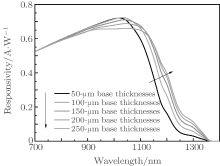
Figure 4 illustrates the effect of the base thickness on the device responsivity. It is shown that the responsivity decreases as the base thickness increases before the wavelength reaches 1040 nm. When the wavelength is 1000 nm, the responsivities of the photodetectors with 50 nm and 250 nm in base thickness are 0.717 A/W and 0.656 A/W, respectively. If the wavelength is larger than 1120 nm, the responsivity increases with the increase of base thickness. This is because the thicker base can adequately absorb the incident near-infrared photons. Especially, the absorption coefficient of silicon material is very weak in the near-infrared zone. Figure 5 illustrates the EQEs of the devices with different values of base thickness. When the wavelength is larger than 1120 nm, the EQE increases as base thickness increases. The thicker base can obtain more electron-hole pairs since more sub-bandgap photons can be absorbed.
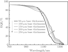 | Fig. 5. Variations of external quantum efficiency with wavelength for different values of base thickness. |
The internal reflection coefficient of the photodetector utilizing the IPV effect should be a crucial parameter that affects the responsivity since those sub-bandgap photons can be adequately absorbed by the reflection behavior. Figure 6 shows the variations of the increment of responsivity Δ R with incident wavelength for different internal reflection coefficients at the back surface of the cell. The improvement of responsivity is defined as the difference between the responsivity with the IPV effect and that without the IPV effect. It can be seen that the improvements of responsivities can attain 0.256 A/W and 0.358 A/W at a wavelength of about 1200 nm when the values of Rb are 0.99 and 0.999, respectively. A big internal reflection coefficient can give rise to a high improvement of responsivity. This is due to the fact that a big internal reflection coefficient increases the opportunity for sub-bandgap photons to be absorbed by weak optical processes in a silicon photodetector and results in more electron photoemissions from the indium level to the conduction band. For the high reflection coefficient, a Bragg reflector structure that reflects nearly 100% of long-wavelength photons was reported.[15]
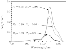 | Fig. 6. Variations of improvement of responsivities Δ R with incident wavelength for different internal reflection coefficients at the back surface of the cell. |
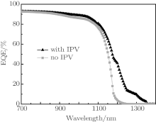 | Fig. 7. Variations of external quantum efficiency of the devices with/without IPV with incident wavelength when Rf is 0.99 and Rb is 0.999. |
Figure 7 shows the variations of the external quantum efficiency of the devices with/without IPV with incident wavelength when Rf is 0.99 and Rb is 0.999. It is obvious that the EQE with IPV is greater than that without IPV. When the wavelength is 1200 nm, the EQE without IPV is almost zero, while that with IPV is 41.1%. It is concluded that the IPV effect raises the quantum efficiency and results in the improvement of the responsivity of a photodetector.
A numerical study is carried out to explore the near-infrared responsivity of silicon photodetectors. It is found that the near-infrared responsivity of silicon photodetectors can be enhanced by the impurity photovoltaic effect. The enhancement of responsivity increases with increasing the indium concentration. Moreover, the responsivities of the photodetectors have some extensions to near-infrared 1360 nm if the indium impurities are introduced. The base thickness of the silicon photodetector has a significant influence on device responsivity. The internal reflection coefficient of the photodetector is crucial to the photodetector responsivity. The improvement of the responsivity can reach 0.358 A/W at a wavelength of about 1200 nm when Rf = 0.99 and Rb = 0.999. Our results may open up a new route to enhancing the responsivity of a photodetector.
| 1 |
|
| 2 |
|
| 3 |
|
| 4 |
|
| 5 |
|
| 6 |
|
| 7 |
|
| 8 |
|
| 9 |
|
| 10 |
|
| 11 |
|
| 12 |
|
| 13 |
|
| 14 |
|
| 15 |
|


