†Corresponding author. E-mail: rxjia@mail.xidian.edu.cn
*Project supported by the National Natural Science Foundation of China (Grant Nos. 51272202 and 61234006) and the Science Project of State Grid, China (Grant No. SGRI-WD-71-14-004).
We study a series of (HfO2) x(Al2O3)1 − x /4H-SiC MOS capacitors. It is shown that the conduction band offset of HfO2 is 0.5 eV and the conduction band offset of HfAlO is 1.11–1.72 eV. The conduction band offsets of (HfO2) x(Al2O3)1 − x are increased with the increase of the Al composition, and the (HfO2) x(Al2O3)1 − x offer acceptable barrier heights (> 1 eV) for both electrons and holes. With a higher conduction band offset, (HfO2) x(Al2O3)1 − x/4H-SiC MOS capacitors result in a ∼ 3 orders of magnitude lower gate leakage current at an effective electric field of 15 MV/cm and roughly the same effective breakdown field of ∼ 25 MV/cm compared to HfO2. Considering the tradeoff among the band gap, the band offset, and the dielectric constant, we conclude that the optimum Al2O3 concentration is about 30% for an alternative gate dielectric in 4H-SiC power MOS-based transistors.
Silicon carbide (SiC) has attractive properties, including a wide band gap (3.26 eV for 4H-SiC) and a high breakdown electric field (2– 3 MV/cm) suitable for high-power switching devices, such as MOSFET.[1– 4] The quality and reliability of the gate insulators are the determining factors in SiC power devices.[5, 6] According to the Gauss law, the most frequently used dielectric at present, SiO2 (ɛ = 3.9), is subjected to fields of 5 MV/cm, which is too much, in the SiC MOS devices at very high applied voltage.[7] To reduce the electric field in the gate oxide, various high k gate dielectric materials have been investigated on the SiC substrate.[8– 11] In addition to a high k value, good thermal stability, high conduction band offset, and relatively large energy gap are key factors to obtain high quality and reliability for the gate oxide. In this study, a series of high-k materials, (HfO2)x(Al2O3)1 − x, are investigated, since they have a higher dielectric constant similar to HfO2, as well as higher crystallization temperature and conduction band offset similar to Al2O3.[12– 14] Intermixing Al2O3 with HfO2 to form HfAlO has several potential advantages for a gate dielectric on 4H-SiC, such as good thermal stability, low gate leakage current, and high breakdown electric field.
4H-SiC substrates with an n-epilayer (doping ∼ 3× 1015 cm- 3) were dipped in a 5% HF solution for native oxide removal. After cleaning, a series of high-k materials (HfO2)x(Al2O3)1 − x were deposited using atomic layer deposition (ALD). The thicknesses of the gate oxides were around 10 nm obtained by the spectroscopic ellipsometer. The X-ray photoelectron spectroscopy (XPS) measurements were carried out to obtain the Al 2p, Hf 4f, O 1s, C 1s, Si 2p, and full spectra using a Thermo SCIENTIFIC ESCALAB 250 spectrometer with Al Kα X-ray source (1486.8 eV). Last, the electrical properties were obtained by current– voltage (I– V) and capacitance– voltage (C– V) characterizations using an Agilent B1500A.
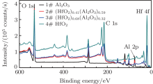
The chemical compositions of the samples are obtained from the XPS full spectra, and the HfO2 mole fractions x are calculated, as listed in Table 1. According to the different x values, the four samples are denoted as 1# Al2O3, 2# (HfO2)0.41(Al2O3)0.59, 3# (HfO2)0.68(Al2O3)0.32, and 4# HfO2, respectively. As shown in Fig. 1, the primary elements are detected in the XPS full spectra, and the different element contents of the samples can be observed visually. For example, for the Hf 4f spectra, the peak area of 4# HfO2 is the largest.
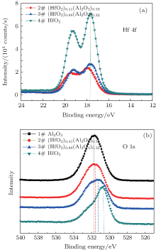
The Hf 4f and O 1s core level spectra for HfO2 and HfAlO films are measured to compare the O and Hf chemical bonding states in the four dielectrics. Figure 2(a) shows the Hf 4f core level spectra for bulk 2# – 4# samples. The elemental content can be represented by the area under the XPS line. The elemental content of Hf decreases with the decrease of the HfO2 mole fraction in Fig. 2(a). It is observed that the core level peak position of Hf 4f shifts to a higher binding energy with an increase of the Al composition. Figure 2(b) shows the O 1s core level spectra for bulk 1# – 4# samples. The O 1s peak in the case of HfO2 is at 530.68 eV and corresponds to the O– Hf bonding. The peak of 1# Al2O3 is at 531.68 eV and corresponds to the O– Al bonding. The peak shifts to a binding energy of 530.8 eV in the case of HfAlO, indicating intermixing of Al2O3 and HfO2 layers and the formation of Hf– O– Al bonding. The HfAlO dielectric is composed of the new chemical bonding, and it has several potential advantages for the gate dielectric on 4H-SiC due to the combination of the advantages of both Al2O3 and HfO2.
| Table 1. Chemical compositions of (HfO2)x(Al2O3)1 − x samples. |
 | Fig. 2. (a) Hf 4f core level spectra of (HfO2)x(Al2O3)1 − x samples, and (b) O 1s core level spectra of (HfO2)x(Al2O3)1 − x samples. |
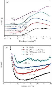
 | Fig. 3. (a) XPS valence band spectra of (HfO2)x(Al2O3)1 − x samples and 4H-SiC substrate. (b) O 1s energy loss spectra of (HfO2)x(Al2O3)1 − x samples. |
The valence band offset Δ Ev, conduction band offset Δ Ec, and energy gap Eg of (HfO2)x(Al2O3)1 − x on 4H-SiC are measured by XPS.[15] The Δ Ev can be determined with the equation

where 


The Δ Ec can be derived by the equation

where Eg(dielectric) is the energy gap of the gate dielectric, and Eg(SiC) is the energy gap of 4H-SiC (3.26 eV). The onset of single particle excitation or band-to-band transition can be used to measure the energy band gap of the film.[17] The Eg of each sample is extracted from the O 1s energy loss spectra for (HfO2)x(Al2O3)1 − x samples. They are obtained by deducting the binding energy at the peak of the O 1s XPS spectra. The Eg of the samples are 7.22 ev, 6.47 eV, 5.91 eV, and 5.29 eV, respectively, which are denoted by the cross points in Fig. 3(b). Then, the Δ Ec of 1# – 4# samples are determined by Eq. (2) to be 1.76 eV, 1.62 eV, 1.11 eV, and 0.50 eV, respectively. The result is in general agreement with the one previously reported in the literature.[17]
The band alignments of (HfO2)x(Al2O3)1 − x on 4H-SiC are compared in Fig. 4. It can be seen that the band offset decreases with the increase of the HfO2 mole fraction x. The Al2O3 on 4H-SiC with the considerable valence and conduction band offsets (1.76 eV, 2.2 eV) indicates higher barrier heights for electrons and holes, compared to HfO2 (0.50 eV, 1.53 eV). HfAlO offers acceptable barrier heights (> 1 eV) for both electrons and holes with a higher dielectric constant k, which makes it a suitable dielectric for 4H-SiC MOS devices.
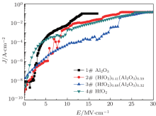
 | Fig. 5. The J– E characteristics of 4H-SiC MOS structures with (HfO2)x(Al2O3)1 − x as the gate dielectrics. Here E = (Vg– VFB) /EOT, wit VFB being the flat-band voltage. |
The current density– electric field curves (J– E) of 4H-SiC MOS structures with 1# Al2O3, 2# (HfO2)0.41(Al2O3)0.59, 3# (HfO2)0.68(Al2O3)0.32, and 4# HfO2 as the gate dielectrics are shown in Fig. 5, which are transformed from the corresponding I– V curves. The electric field is approximately given by (VG– VFB)/EOT, where VG and EOT are the gate voltage and the equivalent oxide thickness with respect to SiO2, respectively. With a higher conduction band offset, 3# (HfO2)0.68(Al2O3)0.32 results in a ∼ 3 orders of magnitude lower gate leakage at an effective electric field of 15 MV/cm and roughly the same effective breakdown field of ∼ 25 MV/cm compared to HfO2. The increase of Al induces an increase of the dielectric constant of the dielectric, which causes a higher gate leakage and a lower effective breakdown field compared to (HfO2)0.68(Al2O3)0.32.
A series of (HfO2)x(Al2O3)1 − x/4H-SiC MOS capacitors have been studied. It is found that the band offset and the band gap are increased with the increase of the Al composition. Considering the tradeoff among the band gap, the band offset, and the dielectric constant, we conclude that the optimum Al2O3 concentration is about 30% for an alternative gate dielectric in 4H-SiC power MOS-based transistors.
| 1 |
|
| 2 |
|
| 3 |
|
| 4 |
|
| 5 |
|
| 6 |
|
| 7 |
|
| 8 |
|
| 9 |
|
| 10 |
|
| 11 |
|
| 12 |
|
| 13 |
|
| 14 |
|
| 15 |
|
| 16 |
|
| 17 |
|
| 18 |
|


