
Influences of fringing capacitance on threshold voltage and subthreshold swing of a GeOI metal-oxide-semiconductor field-effect transistor*
[Fan Min-Min, Xu Jing-Ping† , Liu Lu, Bai Yu-Rong, Huang Yong]
, Liu Lu, Bai Yu-Rong, Huang Yong]
|
|


†Corresponding author. E-mail: jpxu@mail.hust.edu.cn
*Project supported by the National Natural Science Foundation of China (Grant No. 61274112).
Models of threshold voltage and subthreshold swing, including the fringing-capacitance effects between the gate electrode and the surface of the source/drain region, are proposed. The validity of the proposed models is confirmed by the good agreement between the simulated results and the experimental data. Based on the models, some factors impacting the threshold voltage and subthreshold swing of a GeOI metal-oxide-semiconductor field-effect transistor (MOSFET) are discussed in detail and it is found that there is an optimum thickness of gate oxide for definite dielectric constant of gate oxide to obtain the minimum subthreshold swing. As a result, it is shown that the fringing-capacitance effect of a short-channel GeOI MOSFET cannot be ignored in calculating the threshold voltage and subthreshold swing.
In order to maintain the scaling trend of complementary metal oxide semiconductor (CMOS) circuits in accordance with Moore's law, it is suitable to replace the conventional SiO2/Si system with innovative device structures and new materials. The recent development of high-κ gate dielectrics suitable for Ge substrate and the high carrier mobility of Ge make GeOI metal-oxide-semiconductor field-effect transistor (MOSFET) has become a potential candidate for a new generation of CMOS technology. However, the use of high-κ gate dielectrics makes the fringing-capacitance effects of short-channel MOSFET more significant.[1– 3] Bansal et al.[2] and Feng et al.[4] studied the fringing capacitance only between the right/left edge of gate electrode and the surface of source/drain region. Kumar et al.[5] studied the fringing capacitance only between the bottom of the gate electrode and the surface of source/drain region. Feng et al.[4] and Kumar et al.[5] also studied the influence of fringing capacitance on threshold voltage of MOSFET. However, they did not consider the edge-effect in capacitance of non-parallel plate capacitor when using the conformal mapping transformation. All of these models only considered the effect of some fringing capacitance on the threshold voltage, and they have ignored the fringing capacitance between the top of the gate electrode and the surface of the source/drain region. Moreover, the influence of the fringing capacitance on the subthreshold swing of MOSFET is hardly involved.
In this work, all kinds of fringing capacitance between the gate electrode and the surface of source/drain region and the edge-effect in capacitance of non-parallel plate capacitor are considered to build models of both the threshold voltage and the subthreshold swing. Our simulated results are in good agreement with the experimental data.
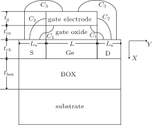
The fringing-capacitance model of the GeOI MOSFET is shown in Fig. 1, where C1 is the fringing capacitance between the bottom of the gate electrode and the surface of source/drain region, C2 is the fringing capacitance between the right/left edge of gate electrode and the surface of the source/drain region including the edge effect in capacitance of non-parallel plate capacitor, C3 is the fringing capacitance between the top of the gate electrode and the surface of the source/drain region, L is the channel length, and La is the width of the source/drain region.
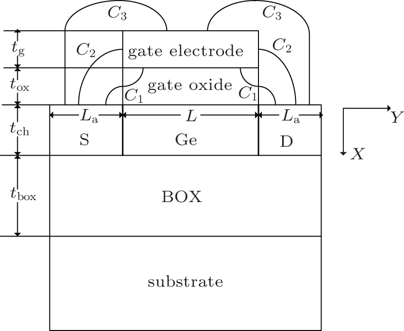 | Fig. 1. Schematic fringing-capacitance model of a GeOI MOSFET. |
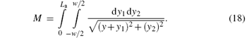
Fringing capacitance C1 can be expressed as[5]

where kox is the dielectric constant of the gate oxide and ks is the dielectric constant of the spacer. Here, C2i is defined as the fringing capacitance between the right/left edge of gate electrode and the surface of source/drain region without the edge effect in the capacitance of the non-parallel plate capacitor, which can be expressed as[4]

where tox is the thickness of gate oxide and tg is the thickness of gate electrode. The C2fi is defined as the fringing capacitance generated by the edge effect in the capacitance of the non-parallel plate capacitor. It can be calculated by Schwarz– Christoffel transformation[6] and expressed as

Therefore, C2 can be written as

and C3 can be obtained by conformal mapping transformation by assuming that the length of the parallel plate capacitor on top of the gate electrode is equal to La,

Thus, the total fringing capacitance Cof between the gate electrode and the surface of source/drain region is the sum of C1, C2, and C3.
Kumar et al.[5] assumed that the charge distribution induced in the source and drain regions due to the fringing electric field is uniform, with the charge densities of source and drain regions Qs and Qd given, respectively, by


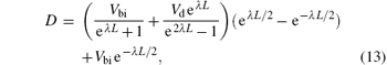
where Vbi is the built-in potential of source/drain-channel junction, Vg is the gate voltage, Vfb is the flat-band voltage of the front gate, and Vd is the drain voltage. The surface potential due to this uniform charge distribution along the channel can be expressed as

where kch is the the dielectric constant of channel. According to Young's model, [7] the surface potential of a GeOI MOSFET without fringing capacitance can be expressed as

where

B = Vbi − C − A, C = − β /α , and α , β can be written as
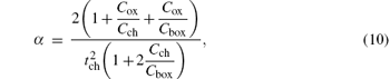
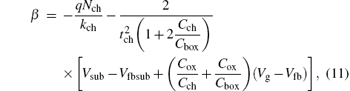
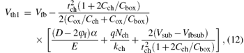
where Cox is the gate oxide capacitance, Cch is the channel capacitance, Cbox is the buried oxide capacitance, tch is the channel thickness, Nch is the channel doping concentration, Vsub is the substrate voltage, and Vfbsub is the flat-band voltage of the back gate. The threshold voltage Vth1 without considering the fringing capacitance is defined as ϕ s max = 2φ f (ϕ s max is the maximum surface potential occurred at ymax = L / 2 and φ f is the Fermi potential) for small Vd, and can be written as

When the fringing capacitance is considered, the surface potential ϕ 's (y) can be modified as

Thus, the threshold voltage with the fringing capacitance Vth2 can be gotten by setting ϕ 's max = 2φ f,

where
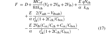
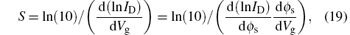
The charges induced in the source and drain regions introduce an additional surface potential in the channel region and impact the subthreshold swing. The subthreshold swing can be expressed as
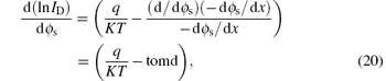
with

where K is the Boltzmann constant, tomd is an intermedium variable, and Es is the electric field at the channel surface and can be written as

It is worth pointing out that the use of high-κ gate dielectrics would give rise to the problem of carrier-mobility degradation due to the coupling of soft optical phonon modes in high-κ to the inversion channel charge carriers, [8, 9] i.e., phonons scatter electrons in channel, which, however, is not involved in the above models and will be investigated in detail in our next-step work for the GeOI MOSFET.
Based on the above model, the threshold voltages and subthreshold swings with/without the fringing-capacitance effect are simulated and compared with the experimental data, [10, 11] as shown in Fig. 2. It can be seen that the subthreshold swing considering all of the fringing capacitance is closer to the experimental data than the other two simulated results (the inversion electron density is considered when solving the Poisson equation of Young's model), and the threshold voltage considering all the fringing capacitance is also more accurate than the other two models, especially for L< 70 nm, indicating that all fringing capacitance including C2fi and C3 must be considered to accurately simulate the threshold voltage and subthreshold swing of a small GeOI MOSFET.
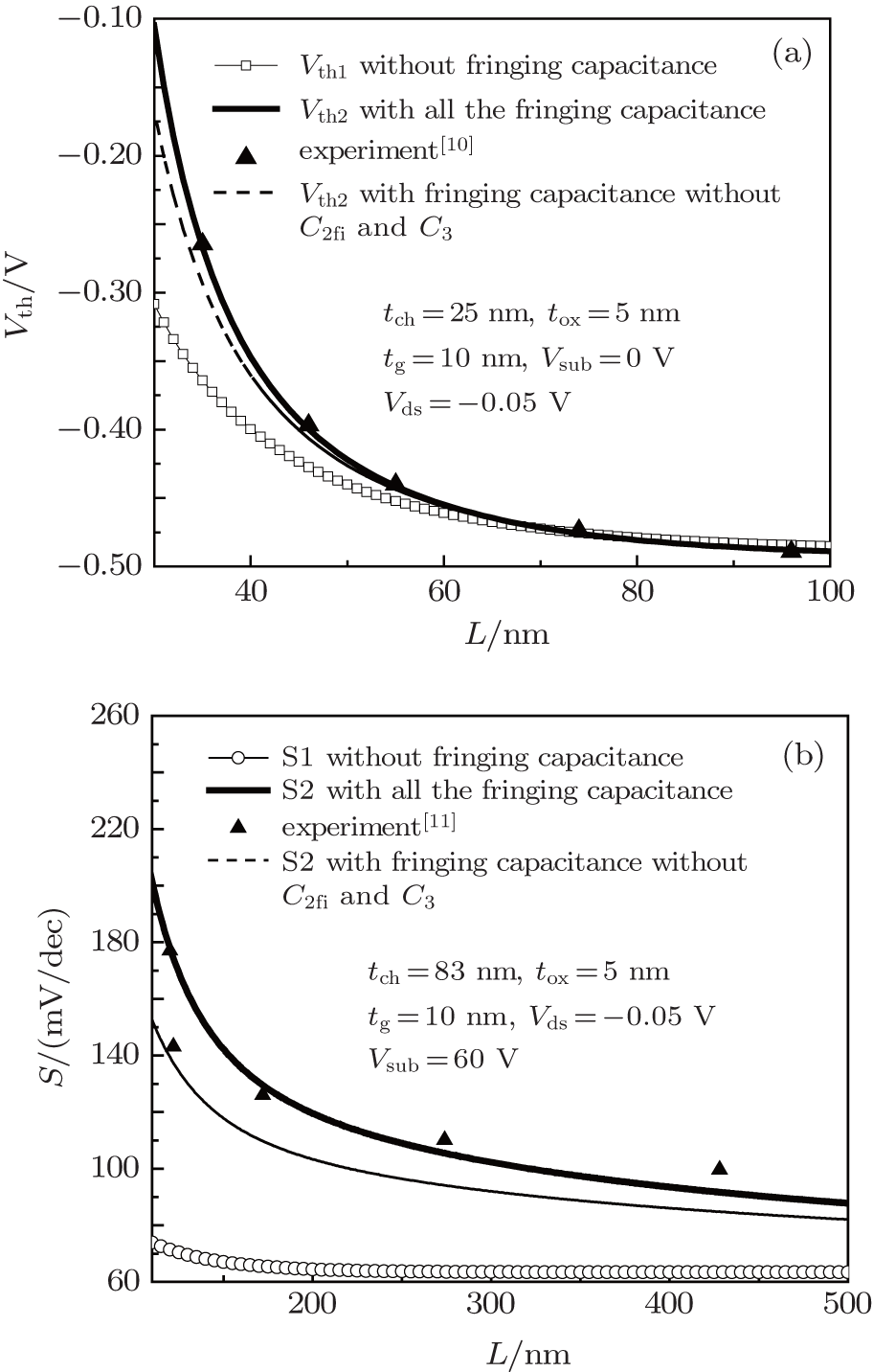 | Fig. 2. Simulated and experimental threshold voltages (a) and subthreshold swing with/without the fringing-capacitance effect (b). |
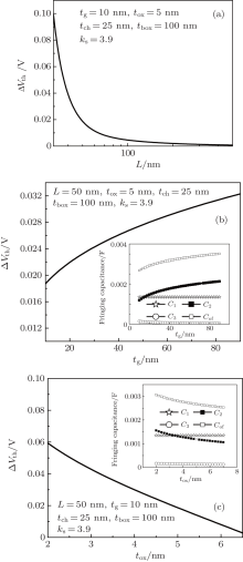
The Δ Vth is defined as the difference between the threshold voltages with/without the fringing capacitance to further evaluate the influences of the fringing capacitance on the threshold voltage. Figures 3(a)– 3(c) show the influences of channel length L, gate electrode thickness tg, and gate oxide thickness tox on Δ Vth, respectively. As can be seen from Fig. 3, the effect of the fringing capacitance on threshold voltage is enhanced as the channel length shrinks due to the shortened distance between the middle of the channel and the fringing field in the source/drain region; Δ Vth is increased with increasing tg due to the increased fringing capacitance C2, as shown in the inset in Fig. 3(b). Although C3 is also decreased with increasing tg, C3 is much smaller than C2 and the total fringing capacitance Cof is dominated by C2. Similarly, as gate oxide thickness decreases, Δ Vth is increased, as shown in Fig. 3(c). In other words, a thinner gate electrode and thicker gate oxide can alleviate the effects of the fringing capacitance on the threshold voltage of GeOI MOSFET.
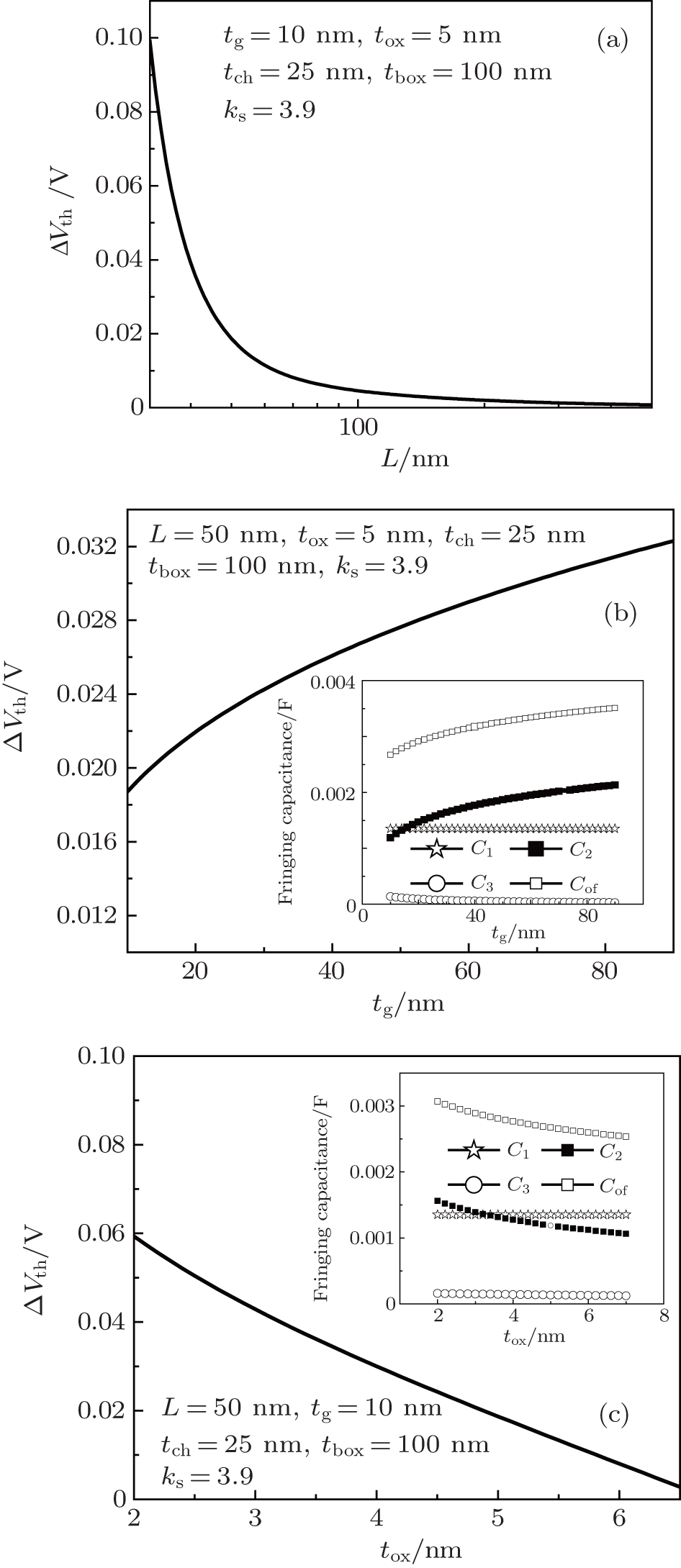 | Fig. 3. Influences of the fringing capacitance on threshold voltage for different (a) channel lengths, (b) gate electrode thickness, (c) gate oxide thickness. The insets show variation of fringing capacitance as a function of (b) gate electrode thickness, (c) gate oxide thickness. |
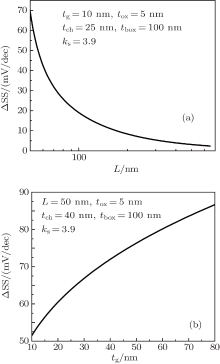
The Δ SS is defined as the difference between the subthreshold swings with/without the fringing capacitance. Figures 4(a) and 4(b) depict the changes of Δ SS with the Ge channel length and gate electrode thickness, respectively. It can be seen from Fig. 4(a) that the influence of the fringing capacitance on subthreshold swing is weakened as the channel length increases because the potential in the channel induced by the fringing field is decreased. Δ SS is increased with increasing tg, as shown in Fig. 4(b), due to the same reason as Δ Vth in Fig. 3(b).
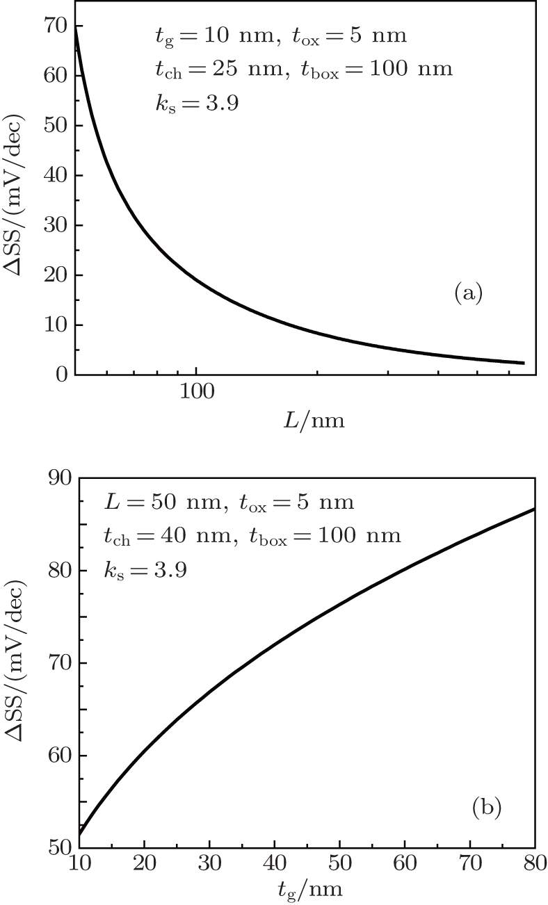 | Fig. 4. Influences of the fringing capacitance on subthreshold swing for different (a) channel lengths and (b) gate electrode thicknesses. |
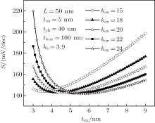
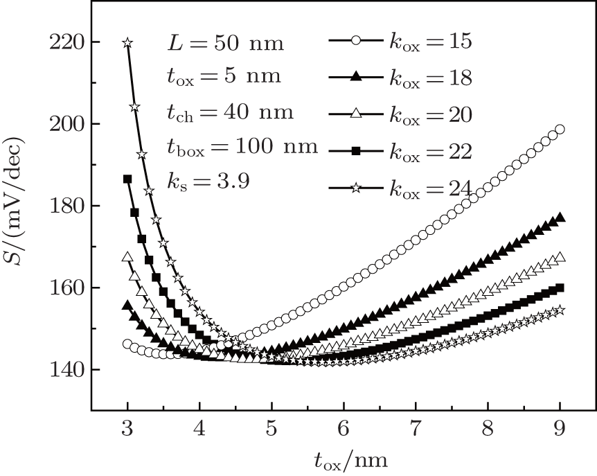 | Fig. 5. Variation of subthreshold swing with fringing capacitance as a function of gate oxide thickness under different dielectric constants of gate oxide. |
Figure 5 shows the change of the subthreshold swing with tox for different dielectric constants of gate oxide when fringing capacitance is considered. In simulation, the subthreshold current controlled by ϕ s remains the same for different tox and kox, and so the gate voltage Vg is assumed to be Vg= Vth2+ 0.05 to make the MOSFET in the subthreshold region with ϕ s = − 0.49. It is found from Fig. 5 that as tox increases, the subthreshold swing is decreased first and it then increased. This happens because when Vth2 is decreased, Es is increased due to the same ϕ s for different tox, so that tomd and d ϕ s /d Vg are decreased as tox increases, and thus the subthreshold swing as a function of tox exhibits a parabolic curve. In addition, It can be seen that the minimum subthreshold swing occurs at different tox for different kox. Therefore, there is an optimal tox for definite kox to obtain the best subthreshold behaviors, e.g., tox is in the range of 3.6– 5.7 nm for 15 ≤ kox≤ 24. Moreover, it can be observed that the larger the kox is, the smaller the change of subthreshold swing with tox beyond the optimal tox, which permits a wider-range for the choice of the gate oxide thickness.
Various kinds of fringing capacitance between the gate electrode and the surface of source/drain region are considered to build models of the threshold voltage and subthreshold swing of GeOI MOSFET. Good agreement between the simulated results and experimental data is obtained, confirming the validity of the proposed models. The simulated results show that the fringing-capacitance effect cannot be ignored for a short-channel GeOI MOSFET, and the thin gate electrode can alleviate the impacts of fringing capacitance on threshold voltage and subthreshold swing, and there is an optimal thickness of gate oxide for the definite dielectric constant of the gate oxide for achieving the best subthreshold behaviors.
| 1 |
|
| 2 |
|
| 3 |
|
| 4 |
|
| 5 |
|
| 6 |
|
| 7 |
|
| 8 |
|
| 9 |
|
| 10 |
|
| 11 |
|