Corresponding author. E-mail: tzhu@aphy.iphy.ac.cn
Project supported by the National Basic Research Program of China (Grant No. 2012CB933102) and the National Natural Science Foundation of China (Grant Nos. 11079052, 11174354, and 51172080).
An obvious weak localization correction to anomalous Hall conductance (AHC) in very thin CoFeB film is reported. We find that both the weak localization to AHC and the mechanism of the anomalous Hall effect are related to the CoFeB thickness. When the film is thicker than 3 nm, the side jump mechanism dominates and the weak localization to AHC vanishes. For very thin CoFeB films, both the side jump and skew scattering mechanisms contribute to the anomalous Hall effect, and the weak localization correction to AHC is observed.
Anomalous Hall effect (AHE) has continually received a certain amount of attention in both fundamental research and device application for decades.[1– 5] The Hall resistivity in a magnetic thin film consists of two terms: one represents the ordinary Hall effect and the other represents the AHE, which is much larger than the former. The current understanding of AHE's mechanism in a clean ferromagnetic material is focused on three proposed mechanisms:[4] the intrinsic mechanism, [5, 6] extrinsic skew-scattering (SS), [7] and side-jump (SJ).[8] The intrinsic AHE was first interpreted to stem from spin– orbit coupling in the crystal band structure, [6] but now has been reinterpreted in terms of the Berry curvature of the occupied Bloch states.[5]
In general, a scaling relation between the anomalous Hall resistivity (ρ AH) and longitudinal resistivity (ρ xx)

is approximately valid, and it is used to investigate the origin of AHE.[9] Here, the first term represents the contribution of SS and the second term represents the contribution of SJ. However, the reduced dimensionality can induce quantum correction on AHE, [10– 14] particularly in the presence of disorder. The resistivity shows an obvious minimum at low temperature due to the weak localization (WL) effect.[13, 14] Thus, the above simple scaling relation between ρ AH and ρ xx is not valid in the whole temperature region. So far, there has been no systematic study of the AHE mechanism in highly disordered thin film.
Here we have investigated the anomalous Hall effect in CoFeB thin film with thickness down to 1.7 nm. The reason we chose CoFeB is that it is the most promising candidate to serve as the magnetic sensing layer in spintronic devices.[15– 17] However, CoFeB thin film deposited using a standard sputtering process is always amorphous and shows a resistivity minimum at low temperature.[18] Thus the effect of quantum correction should be considered when the device works at low temperature. In this paper, we report an obvious weak localization correction to anomalous Hall conductance (AHC) when the film is thinner than 3 nm. We also find that both the weak localization to AHC and the mechanism of the anomalous Hall effect in CoFeB are related to its thickness.
Amorphous Co40Fe40B20 film samples (1.7 nm– 10.5 nm) were deposited on thermally oxidized silicon wafer by DC magnetron sputtering with a base pressure of 5× 10− 6 Pa. The sputtering details can be seen elsewhere.[17] All the CoFeB films were capped with a 3-nm-thick MgO to prevent oxidation. High purity MgO (99.99%) and Co40Fe40B20 (99.9%, Functional Materials International, Japan) were used as the target materials. The layer thickness was identified by an x-ray reflectometer (XRR, Brucker D8) and confirmed by XRR obtained at 1 W 1 A, Beijing Synchrotron Radiation Facility (BSRF). Hall-bar patterned films were used for the resistivity and Hall measurements from 5 K to 300 K with a Quantum Design® physical property measurement system (PPMS). To exclude the ordinary Hall effect, we define anomalous Hall resistivity as ρ AH, which is obtained as the zero field extrapolation of the high field.
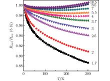
Figure 1 shows the temperature dependence of the normalized sheet resistance Rxx/Rxx (5 K) for the CoFeB films down to 1.7 nm. Similar to the traditional amorphous metallic alloys, [19] the temperature dependence of Rxx for the CoFeB thin film shows an obvious resistance minimum at low temperature, which is accompanied by a change from a negative temperature coefficient of resistivity (TCR) to a positive TCR. Figure 2 shows the representative temperature dependence of Rxx/Rxx (5 K), which can be further fitted by using a single logarithmic form, ln(T/T0), in the temperature ranging from 5 K to 50 K. This indicates the WL effect in the amorphous CoFeB thin films at low temperature. A similar characteristic has already been found in these highly disordered thin films.[11, 14]
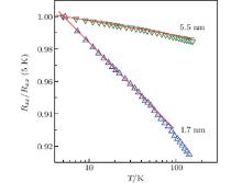 | Fig. 2. Temperature dependencies of Rxx/Rxx (5 K) for CoFeB of 1.7 nm (up triangles) and 5.5 nm (down triangles). The solid lines are fitted by using a single logarithmic form, ln(T/T0). |
In order to further study the WL effect in amorphous CoFeB thin films, we define the normalized relative change following the work in Refs. [10] and [11], Δ N(Qij) = (1/L00R0)(δ Qij/Qij), with respect to our reference temperature T0 = 5 K < T, where δ Qij = Qij(T)− Qij(T0) and Qij refers to either resistance Rxx, Rxy (RAH) or conductivity σ xx, σ xy (σ AH). Here, we defined σ xx≅ 1/ρ xx and 

Due to δ Rxx ≪ R and RAH ≪ Rxx, the anomalous Hall conductance σ AH obeys

Figure 3 shows the representative temperature dependencies of Δ N(σ AH), together with Δ N(Rxx) and Δ N(RAH) for comparison. Apparently, both Δ N(Rxx) and Δ N(RAH) obey the dependence of − ln(T/T0). However, Δ N(σ AH) shows different temperature dependences, i.e. Δ N(σ AH) ≈ 0 for R0 = 308 Ω (t = 5.5 nm), but increases with temperature for R0 = 2.0 kΩ (t = 1.7 nm). For the former film, the relation of 2AR ≈ AAH is valid. Here R0 represents the sheet resistence at 5 K. Similar relations of 2AR = AAH and Δ N(σ AH) = 0 have been reported for the Fe granular film with R0 = 140 Ω .[11] For the latter film, the temperature dependencies of Δ N(Rxx) and Δ N(RAH) nearly overlap each other, indicative of AR ≈ AAH ≈ 1, an overlap quite similar to that in the previous granular Fe film with high disorder (R0 = 2.7 kΩ ).[11]
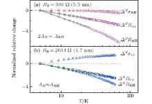 | Fig. 3. Normalized relative change Δ NRxx (blue open triangles), Δ NRAH (red open squares), and Δ ^Nσ AH (green open circles) for R0 = 308 Ω (a) and 2034 Ω (b) respectively. The dashed lines are guides for the eye. The solid lines are results of fitting by using Eq. (2). |
Figure 4 shows the three fitting parameters, AR, AAH, and 2AR − AAH, for CoFeB thin films with R0 varying from 184 Ω to 2.0 kΩ . AR is always equal to unity whereas the R dependencies of AAH and 2AR − AAH are separated as two parts. In the range of R0 ≤ 700 Ω (t ≥ 3 nm), the WL correction to AHC is negligible. For thin CoFeB films (t < 3 nm), the prefactor of Δ Nσ AH, 2AR − AAH is nonzero, which indicates the WL correction to AHC. The thickness-dependence of the WL correction behavior suggests that the AHE mechanism is thickness-dependent. Indeed, a theory based on a granular model of AHC predicts that the SS and SJ mechanisms have different roles in the localization corrections.[11, 20– 22] In this theory, [11] the WL correction to AHC is described by

where rAH is the ratio of two different mechanisms contributing to AHE, namely, the side jump 


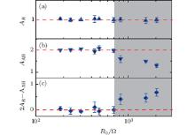 | Fig. 4. Dependence of the coefficients AR (a) and AAH (b) as defined in Eq. (2), and of 2AR − AAH (c) on the sheet resistance R0. The dashed lines are guides for the eye. The grey range indicates WL corrections to AHC. |
As we mentioned above, the AHE mechanisms can be generally determined by the simple relation between ρ AH and ρ xx. If the sample has a high Curie temperature, such as Fe, the AHE mechanisms can be directly investigated from the relationship between ρ AH and ρ xx.[9] Otherwise, a temperature-dependent factor f(T) should be considered.[4] Thus, the determination of the AHE mechanism is strongly related to the accuracy of magnetization measurement of the samples. As for the CoFeB thin films, f(T) is almost equal to 1 at low temperature.[23] We can neglect the effect of the temperature-dependent factor if we only focus on the temperature region of the WL effect, which is normally below 40 K in our case. In other words, equation (1) is valid when T < 40 K. Because ρ AH ≪ ρ xx equation (1) is also rewritten as

The first term comes from the SS mechanism and the second from the SJ mechanism.
Figure 5 shows the disorder factor R0 dependence of rAH. The representative σ xx dependencies of σ AH at low temperature are plotted in the inset. The solid lines are the results of fitting by using Eq. (5). It is readily apparent that the relationship between σ AH and σ xx is thickness-dependent. For the very thin film, for example t = 2 nm, both the SS and SJ mechanisms contribute to the AHC. On the other hand, it is almost scattering-independent for the thick film. Thus, the solid squares in Fig. 4 are the ratio of 
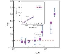 | Fig. 5. The disorder factor R dependence of rAH. The solid squares are the ratio of  |
In summary, an obvious weak localization correction to anomalous Hall conductance in very thin CoFeB film is reported. We find that in CoFeB films, both the weak localization to AHC and the mechanism of the anomalous Hall effect are related to the film thickness. When the film is thicker than 3 nm, the side jump mechanism dominates and the weak localization to AHC vanishes. Otherwise, both side jump and skew scattering mechanisms contribute to the anomalous Hall effect and the weak localization correction to AHC is observed for very thin CoFeB films.
A portion of this work is based on the data obtained at 1 W 1 A, BSRF. Zhu Tao gratefully acknowledges the assistance of scientists of the Diffuse x-ray Scattering Station during the experiments.
| 1 |
|
| 2 |
|
| 3 |
|
| 4 |
|
| 5 |
|
| 6 |
|
| 7 |
|
| 8 |
|
| 9 |
|
| 10 |
|
| 11 |
|
| 12 |
|
| 13 |
|
| 14 |
|
| 15 |
|
| 16 |
|
| 17 |
|
| 18 |
|
| 19 |
|
| 20 |
|
| 21 |
|
| 22 |
|
| 23 |
|


