1. IntroductionInGaN alloys have been studied intensively as potential materials for active layers in light emitting diodes (LEDs) and laser diodes (LDs) because of the advantage of their tuning ability in the alloy band-gap.[1– 4] However, due to the large discrepancy in atomic size between indium and gallium, and a large lattice mismatch of 11% between InN and GaN, either a phase separation or a slight composition fluctuation always occurs in the InGaN epilayer, especially in InGaN epilayers with higher In concentrations.[5, 6] It has been reported that a strong-phase-separated InGaN/GaN multiple quantum well (MQW) LED can produce a dual light wavelength spectrum with blue and green emissions.[7– 9] In such a structure, the blue light is assigned to the low-In-content InGaN matrix, whereas the green light originates from high-In-content region which acts as a quasi-quantum dot (QD). The temperature dependences of these two emissions show that the carriers inside individual components of the phase structure (i.e., the InGaN matrix region and QD region) initially relax from a shallower localized state to a stronger localized state, to then be thermalized to higher levels as temperature increases. Although the localized carriers in InGaN alloy are considered to prevent them from reaching non-radiative recombination sites while playing an important role in their spontaneous emission, [10– 13] the emission mechanism related to both the InGaN matrix and the QDs is still not clearly understood.
In this research an InGaN/GaN MQW LED with green and blue emissions is developed, whose optical behavior is studied through the excitation power dependences of these two emissions at different temperatures. For a low excitation power range, the experimental results interestingly show that both QD-related green emission and matrix-related blue emission are dominated by the combined action of Coulomb screening and localized state filling effect at 6 K. However, at 300 K, QD-related green emission is influenced by the carriers transferring from the shallower QDs to deeper QDs by tunnelling.
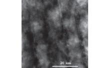
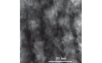
3 Results and discussionFigure 1 illustrates the cross-sectional HRTEM image of the sample. One can easily distinguish between the barriers and wells in an active region by fluctuations in the indium composition. The uniform distribution of areas with strong black/white contrast within the InGaN well layers implies high strain, which may originate from coherent interfaces between the surrounding InGaN matrix and the In-rich QDs.
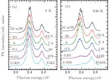
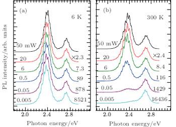
Figure 2 demonstrates the excitation power-dependent PL spectra of the sample measured from 50 mW to 0.001 mW at both 6 K and 300 K. At both temperatures, two InGaN-related emissions are observed at about 2.4 eV (516 nm) and 2.7 eV (459 nm) under an excitation of 50 mW. The two emissions are considered to originate from a strong phase separation, as evinced by the HRTEM image in Fig. 1. The lower energy side peak (green) was attributed to the In-rich QD-related transition (symbolized as PD) and the higher energy side peak (blue) to the InGaN matrix-related near-band-edge transition (symbolized as PM). It is found from Fig. 2 that as excitation power decreases from 50 mW to 0.001 mW, the green emission peak PD decreases rapidly in intensity compared with the blue peak PM at 300 K. However, the decrease was not clearly observed at 6 K.
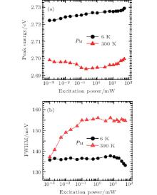
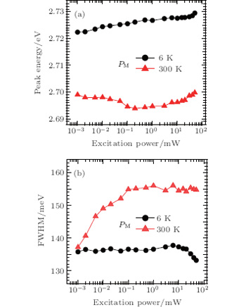
To elucidate the transfer and recombination process of the carriers inside these two phase-separated structures, the excitation power dependencies of the peak energy and full-width at half-maximum (FWHM) for emissions PM and PD in a wider temperature range are summarized in Figs. 3 and4, respectively, where Gaussian fitting is used to remove the Fabry– Perot fringes, and obtain accurate peak energies and FWHMs. For the PM emission at 6 K, shown in Fig. 3, as excitation power increases from 0.001 mW to 50 mW, the peak energy increases monotonically, accompanied by an almost unchanged FWHM below 10 mW and then a narrowing FWHM up to 50 mW. This behavior is different from that of the blue InGaN/GaN MQW obtained under the same measurement conditions, [14] where PL measurements at 6 K and at low excitation power indicate that with increasing the excitation power the PM peak energy shows a monotonic increase accompanied by narrowing FWHM. This indicates that the InGaN matrix-related recombination process in the blue InGaN/GaN MQWs is dominated by a Coulomb screening of the quantum confined Stark effect (QCSE) that is induced by a piezoelectric field resulting from the lattice mismatch between the InGaN layer and the GaN layer, [15, 16] since the increasing photo-generated carrier density weakens the QCSE, which results in the increased peak energy and the narrowed FWHM with an increase in the excitation power.[8, 14, 15, 17]
Based on the experimental evidence above, the behavior of the PM emission in the low excitation power range below 10 mW and at 6 K, shown in Fig. 3, may be explained. For green and blue InGaN/GaN MQWs with a higher indium component than the blue MQWs, a large number of localized centers due to a stronger indium composition fluctuation are present in the InGaN matrix, leading to an enhancement of the band-filling effect of the localized state with respect to the Coulomb screening effect.[14] As a result, the band-filling effect and Coulomb screening effect together dominate the recombination process of the InGaN matrix, leading to the increase in the PM peak energy, accompanied by the almost unchanged FWHM in the low excitation power range below 10 mW and at 6 K (Fig. 3). The strong indium composition fluctuations in the green and blue InGaN matrix are evinced by their wider FWHM (∼ 135 meV), as shown in Fig. 3, than in the blue MQW (below ∼ 63 meV), as shown in Ref. [14]. However, the narrowing of PM peak FWHM with further increasing the excitation power above 10 mW at 6 K, could be attributed to the dominant Coulomb screening effect due to the increasing number of photo-generated free carriers. On the other hand, at high temperatures, especially at 300 K, the PM peak energy shows a monotonic decrease accompanied by the broadening of the FWHM as excitation power increases from 0.001 mW to 0.2 mW (Fig. 3), reflecting that the defect-related non-radiative recombination dominates the recombination process.[17] With the further increase of excitation power above 0.2 mW, the non-radiative centers in the InGaN matrix become practically saturated and the radiative recombination begins to dominate the recombination process of the InGaN matrix. Therefore, the PM peak energy shows a monotonic increase, accompanied by an almost unchanged FWHM, similar to that discussed at 6 K and in the low excitation power range below 10 mW in Fig. 3.
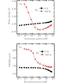
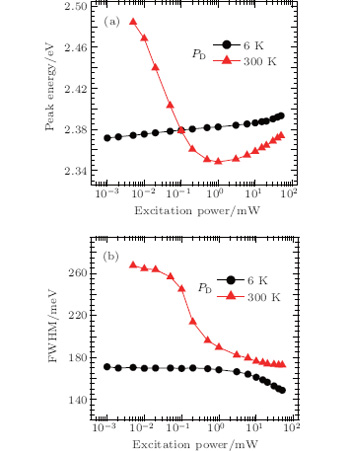
On the other hand, for the PD emission shown in Fig. 4, as excitation power increases from 0.001 mW to 50 mW at 6 K, the PD peak energy shows a monotonic increase, accompanied first by an unchanged FWHM below 1 mW, and then by a narrowing FWHM from 1 mW to 50 mW. The behavior is similar to the 6-K excitation power dependences of the PM peak energy and FWHM shown in Fig. 3, and can be explained by the fact that as excitation power increases from 0.001 mW to 50 mW at 6 K, the PD emission process is dominated first by the combined action of the Coulomb screening effect of QCSE induced by a piezoelectric field resulting from the high In content inside the QDs and the state-filling effect of the QDs below 1 mW, and then by the Coulomb screening effect of QCSE up to 50 mW. However, at high temperatures, especially at 300 K, it is found from Fig. 4 that unlike the case at 6 K, with the increase of excitation power both the PD peak energy and FWHM show a significant decrease in the low excitation power range from 0.001 mW to 1 mW. This behavior is explained neither by the screening of QCSE nor by the state-filling effect of the QDs, since the former would result in a blue-shift of peak energy while the latter would lead to the broadening of FWHM. We cannot attribute this behavior simply to a heating effect, which would result in a significant increase of FWHM.[18] Moreover, the many-body effect is also excluded because it would result in the broadening of the low-energy tail of the PD emissions due to the Coulomb interactions.[19]
However, the aforementioned excitation power behavior of the PD emission at 300 K can be explained as follows: unlike the case at 6 K, at high temperatures, especially at 300 K, the localized carriers inside the QDs are thermally activated and occupy the higher-energy levels of the localized states, thus resulting in the increase of PD peak energy accompanied by the broadening of FWHM at the lowest excitation power compared with the case at 6 K (Fig. 4). As excitation power increases from 0.001 mW to 1 mW at 300 K, increasing number of carriers and excitons are scattered away from the shallower localized QDs and they preferentially transfer into deeper localized QDs by tunneling. Therefore, the overall tendency of the carrier distribution, that is, the weight of carrier distribution among the QDs, moves towards lower QD energies, thereby reducing the resulting energy and shrinking the FWHM of the PD peak. The strong inhomogeneity of the indium content and size of the QDs inferred from the large FWHM of the PD peak shown in Fig. 4, also support the above mentioned viewpoint. Here, it should be pointed out that no carrier transfer among the QDs by tunnelling at 6 K is shown in Fig. 4, which might be due to the fact that the localized effect of the QDs at 6 K is stronger than at 300 K. In addition, with a further increase in the excitation power above approximately 1 mW at 300 K, the PD peak energy shows a significant increase, accompanied first with a slow decrease of FWHM and then with an almost constant FWHM. This behavior might result from the fact that with an increase in the excitation power, the carrier transfer among the QDs is gradually suppressed due to the more significant increase in the number of the carriers inside the deep localized QDs than inside the shallower localized QDs, while the combined action of the Coulomb screening effect of QCSE and the state-filling effect of the QDs starts to dominate the PD emission process.
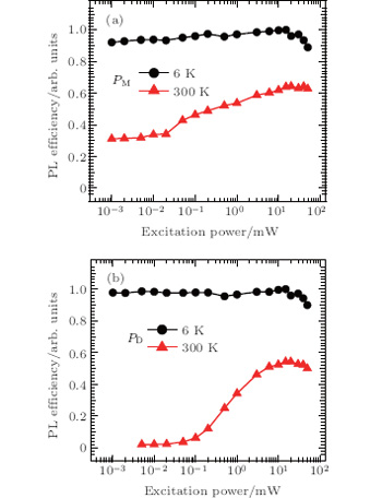
To further investigate the carrier transfer and recombination mechanism of the InGaN/GaN MQWs, figure 5 shows the PL efficiencies of PM and PD, each as a function of excitation power at 6 K and 300 K. The PL efficiency is defined as the integrated PL intensity divided by the excitation power. The maximum PL efficiency value for each emission (i.e., PM or PD) is determined to be nearly 100%. It is found from Fig. 5 that with an increase in the excitation power below approximately 10 mW, the PL efficiencies for both the emission peaks remain almost constant at 6 K and increase at 300 K. It is also noticed that the PD emission shows a more significant increase in PL efficiency than the PM emission at 300 K. The constant PL efficiencies at 6 K for both emission peaks are attributed to the radiative recombination dominating the emission process of MQWs.[17] However, the increasing of PL efficiency for the PM emission at 300 K is due to the recombination mechanism conversion from non-radiative recombination to radiative recombination, while the significantly increasing PL efficiency for the PD emission at 300 K is attributed mainly to the transfer of the carriers from the shallower QDs to the deeper QDs since the transfer significantly enhances the radiative recombination rate of these carriers. Moreover, with a further increase in the excitation power above approximately 10 mW, these PL efficiencies for both emissions show a slight decrease up to 50 mW at all temperatures (Fig. 5), reflecting the fact that the radiative recombination becomes gradually saturated. The experimental results provide an insight into the process of carrier recombination and they also provide a guidance in the fabrication of high-performance InGaN-based LEDs with different wavelengths due to strong phase separation.
4 ConclusionsIn this paper, the PL spectra of an MOCVD-grown InGaN/GaN MQW with clear phase separation are investigated over an excitation power range from 0.001 mW to 50 mW and a temperature range from 6 K to 300 K. Two InGaN-related PL peaks located at around 2.4 eV and 2.7 eV in the full PL spectrum are assigned to the high-In-content QDs and the InGaN matrix, respectively, due to the strong phase separation supported by HRTEM. With an increase in the excitation power in a low excitation power range at 6 K, there is an increased peak energy and an unchanged FWHM for both emission peaks PD and PM, which are attributed to the combined action of the Coulomb screening effect of QCSE and the state-filling effect of localized states. On the other hand, at 300 K and in the low excitation power range, the PM peak energy shows a decrease, which is accompanied with the broadening of FWHM, while the PD peak energy shows a decrease accompanied with the narrowing of FWHM. The former is attributed to the non-radiative recombination process of the carriers in the InGaN matrix, and the latter is due to the fact that increasing numbers of carriers are scattered away from the shallower localized QDs and preferentially transferred into deeper localized QDs by tunnelling, resulting in the weight of carrier distribution among the QDs tending towards lower QD energies. In addition, in the low excitation power range, the unchanged PL efficiencies for both emission peaks at 6 K, are attributed to the fact that the radiative recombination dominates the emission process of MQWs, including the QD regions and the InGaN matrix region. In contrast, the increased PL efficiencies for emission peaks PM and PD at 300 K are due to the recombination mechanism conversion from non-radiative recombination to radiative recombination and to the transfer of carriers among the QDs, respectively. This is in good consistence with the excitation power dependences of the PL peak energy and line-width.


 , Wang Fan