†Corresponding author. E-mail: duhf@hmfl.ac.cn
*Project supported by the National Natural Science Foundation of China (Grant No. 11474290) and the Youth Innovation Promotion Association of the Chinese Academy of Sciences (Grant No. 2015267).
Controllable formation and manipulation of domain walls in one-dimensional (1D) nanostripes underpins a promising type of emergent spintronic device. Magnetic skyrmion is topologically stable whirlpool-like spin texture and is expected to replace familiar domain wall phenomena to build such devices, owing to its prominent features including small size, topological stability and the small critical current required to move it. It is thus essential to understand skyrmions’ properties in such a nanostructured element. In this paper, we mainly give fundamental insight into this issue. Experimental achievements in the formation and stability of individual skyrmions in the nanostripe are outlined in detail.
Conventional magnetic storage in current hard disk drive technology is based on controlled manipulation of magnetic domain by magnetic field. Magnetic recording devices require high-coercivity materials to insure thermal stability at high storage densities. This always leads to the design challenge that small volume (for high density), low coercivity (for good writeability) and high thermal stability cannot all three be optimized at the same time. Hard disk storage is thus fast approaching its limits.[1] The emergent understanding of topological phenomena, along with discoveries of topological materials, offers great opportunities to extend the storage device roadmap further.[2– 5] In magnetic materials, a notable example is the magnetic skyrmion, a swirl-like spin texture with non-trivial topology. The skyrmion is characterized by all the magnetic moments pointing in all directions wrapping a unit sphere (Fig. 1(b)). The peculiar twists of the magnetization within the skyrmion enable efficient couplings with the spin current, leading to topological Hall effects and strong spin-transfer torque effects.[6, 7] Accordingly, the critical current density to move skyrmions is several orders of magnitude smaller than that needed to drive ferromagnetic domain walls.[8– 10] Meanwhile, the size of a single skyrmion is typically on the order of 5 nm– 100 nm, and can be continually tuned by doping.[11] This high mobility, small size and topological stability are all advantages to build skyrmion-based memory or logical devices, in which the designs are all based on the formation and controlled manipulations of individual skyrmions in magnetic nanostructured elements.[12] Among the candidate nanostructures, the nanostripe is the focus of interest, because its geometry is directly relevant to the race-track memory concept, wherein individual skyrmions could be conveniently integrated into this device (Fig. 1(a)). It is therefore an important issue to understand the formation and stability of skyrmions in such a highly confined geometry.
A key ingredient of stabilizing skyrmion phase is the Dzyaloshinskii– Moriya (DM) interaction.[13] DM couplings arise from symmetry-breaking in the crystal lattice of materials including MnSi, FeGe, and Fe1− xCoxSi, [13] which are called helical magnets. The competition between ferromagnetic exchange (FM) and DM couplings leads to the spin helix with a fixed wave-vector, Q, along the high-symmetry crystal axis. If a finite magnetic field B is applied at a temperature T lower than the Curie temperature Tc, it becomes energetically favorable to form a conical phase with Q| | B. At an even higher field, the conical phase transfers into ferromagnetic spin alignment. Both helical and conical states are single-twist magnetic structures since the rotation of their magnetization is only in one direction. In contrast, the magnetization within the skyrmion rotates in two directions, forming double-twist modulations. However, skyrmions occupy only a tiny pocket in the T– B phase diagram, as the temperature is slightly below Tc in bulk compounds. This region of stabilized skyrmion phase would be, to some extent, expanded in the T– B space when the sample is extremely thin. The evolution of spin configurations with varied B and T is shown in Fig. 2 and reflects the common behaviors in helical magnets.[13]
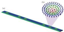 | Fig. 1. Schematic diagram of a skyrmion-based memory device: (a) single skyrmion chain in the nanostripe and (b) spin arrangement in a single skyrmion. |
 | Fig. 2. Common magnetic phase diagram of bulk helimagnets. Panels (a), (b), and (c) schematically represent the spin configurations of helical, conical, and skyrmion phases, respectively, that develop below the Curie temperature Tc. (d) The phase diagram of magnetic structure in bulk helical magnets. Images are taken from Ref. [26]. |
The emergent phenomena in helical magnets have been well explained within the above-mentioned physical model in terms of the DM, ferromagnetic exchange, and external magnetic interaction. The formation of the skyrmion state embedded in the conical states in bulk materials is explained by the thermal fluctuation effect.[14] For the low dimensional helical magnets, the skyrmion state has been observed to show high stability.[15, 16] The present paper will give a general introduction to the highly confined helical magnets, concerning the formation and stability of skyrmions in the FeGe nanostripe. In Section 2, the most used experimental method, i.e., Lorentz transmission electron microscopy (TEM) is discussed, while in Section 3 we step back for a more detailed discussion of the sample fabrication of a nanostripe with desired geometry by using a lift-off method. In Section 4, experimental results with these nanostripes are shown, wherein a new edge-mediated mechanism to create skyrmions has been introduced. But this experimental observation cannot be well explained by current theoretical calculations, as is discussed in Section 5. Finally, an outlook is presented for the future of this field.
The magnetic skyrmion was discovered by neutron diffraction.[2] Just after its discovery, real space observation gave direct images of skyrmions in helical magnet Fe0.5Co0.5Si by using Lorentz transmission electron microscopy.[3] This result is not surprising, because the same group, lead by prof. Tokura, observed helical ground state in the same material Fe0.5Co0.5Si in 2006.[17] Compared with other image techniques for domain wall, the prominent feature in Lorentz TEM lies in its high resolution. As the size of a skyrmion is usually on the order of 3 nm– 100 nm, [11] Lorentz TEM provides a natural tool to image such a small size vortex spin texture.
The principles of Lorentz TEM may be understood classically in terms of the basic interaction between the electron beam and the magnetic fields within and around the magnetic specimen.[18– 21] The most commonly used technique for revealing the domain structures is the Fresnel (or defocus) method. In this method, the objective lens is defocused so that an out-of-focus image of the specimen is formed. A schematic ray diagram of the Fresnel model of Lorentz TEM is shown Fig. 3. For the purpose of illustration, a simple specimen comprising two domains separated by 180° domain walls is assumed.
When the parallel electron beam passes through the area around the domain wall in the thin sample, Lorentz force, defined as

with the electron velocity v and the magnetic induction B, leads to deflections of the electrons. Following the right-hand rule, the electron beams, irradiated on the left and right domains with opposite in-plane magnetization orientations, are deflected in left and right directions, respectively. When imaging the domains in in-focus conditions, these deflecting electrons are focused in the final image plane so that no magnetic contrast appears (Fig. 3(a)). But when the Lorentz TEM is in the over-focused condition, the electron deflection induces a low intensity contrast when electrons are deflected away from the domain wall. This results in the appearance of a dark contrast line in the domain wall region (Fig. 3(b)). Similarly, a bright contrast line appears in under-focused conditions due to the increased electron density caused by overlap (Fig. 3(c)). In this sense, the inversion of the magnetic contrast in the domain wall is observed between the over- and under-focused images. This is the common feature in the Fresnel model images. Note that the out-of-plane magnetic components cannot affect the electron propagation so Lorentz TEM cannot detect the out-of-plane magnetic components. In the Lorentz TEM, the objective lens current can be adjusted continuously to control the magnetic fields applied to the specimen along the z axis.
 | Fig. 3. Schematic ray diagram in a Fresnel image of a ferromagnetic specimen containing two 180° domain walls. (a) In-focus condition: the defected electron beams are focused in the final image plane so that no magnetic contrast appears. (b) and (c) Over- and under-defocus conditions: the defected electron beams lead to dark and bright contrasts, respectively. Image are taken from Ref. [26]. |
As discussed above, visualizing the magnetic contrasts in the domain wall depends on the defocus conditions, and with this understanding, it is possible to reconstruct and map the distribution of the in-plane magnetic components of the domain walls [3]. For this purpose, a commercial software package QPt has been developed, by means of which a series of out-of-focus Lorentz TEM images at different values of the defocus Δ z (in particular + Δ z, − Δ z, and zero) are analyzed by using the transport-of-intensity (TIE) equation

where I(x, y) and ϕ (x, y) stand for the intensity and phase distributions of propagating wave distribution, respectively, and λ is the electron wavelength. On the other hand, according to the Maxwell– Ampé re equations, ϕ (x, y) and magnetization m have a relationship

where e, ℏ , and t are the electron charge, the reduced Planck constant, and the thickness of the sample, respectively, and n is the unit vector parallel to the beam direction. The in-plane magnetic components can be obtained, as the phase shift ϕ (x, y) is known. The intensity gradient ∂ I(x, y)/∂ z can be approximately expressed as Δ I/Δ z, considering that defocus step Δ z is far less than the focal length. A typical process to obtain the magnetic components of the skyrmion phase is shown in Fig. 4.
 | Fig. 4. Schematic diagram of magnetic TIE analysis in the skyrmion state. Three images in the same region under different defocus conditions [(a) in-focus, (b) under-focus, and (c) over-focus. Δ z = 90 μ m] are acquired by using Lorentz TEM. (d) The phase image was created from the three Lorentz micrographs by applying Eq. (1). (e) The in-plane magnetization distribution map was generated from phase image by applying Eq. (2). The color wheel represents the magnetization direction at every point. |
While nanostructured helical magnets appear to be very important, they are unfortunately hard to fabricate. Recent advances have enabled the fabrication of high quality MnSi nanowires synthesized by a chemical method, but the complex crystal structure in the nanowires, such as the parallelogram cross-section and twin boundaries, poses a big challenge in obtaining the skyrmion chain under the applied magnetic field perpendicular to the nanowire, though individual skyrmion cluster states have been identified from magnetoresistance (MR) measurements when the magnetic field is applied along the long axis of the nanowire.[22, 23] Compared with the conventional bottom-up method, current micro- and nano-techniques enable the fabrication of nanoscale samples with desired geometry. In this section, we describe a detailed process for fabricating FeGe helimagnets by using a commercial focused ion beam (FIB) and scanning electron microscopy (SEM) dual-beam system (Helios NanoLab 600i) equipped with a gas injection system (GIS) and micro-manipulator. Figure 5 schematically illustrates the whole process, which goes as follows:
Step 1 Following the standard TEM specimen preparation procedure, [24] a homogeneous FeGe thin narrow membrane with the desired thickness is carved on the surface of FeGe bulk by focused ion beam (FIB) milling. The amorphous surface layer induced by the high energy FIB gallium beam is then reduced to about ∼ 2 nm by polishing the surface with a low energy Ga beam.
Step 2 Using the Gas Injection System (GIS), an amorphous PtCx film is deposited on both sides of the membrane by means of e-beam deposition. These PtCx layers are nonmagnetic and only used to reduce the Fresnel fringes at the edges, as discussed later. Hence, they have no effect on the magnetic properties of the FeGe nanostripe.
Step 3 Using the FIB, the PtCx/FeGe/PtCx sandwich structure is carved to a U-shape to prepare the lift-out.
Step 4 Using the Omniprobe 200+ Micromanipulator, the membrane with two PtCx coating layers is released from the bulk and then transferred onto a clean silicon substrate.
Step 5 Using the standard TEM specimen preparation method again, a PtCx/FeGe/PtCx sandwich structure is fabricated by FIB milling.
Step 6 Using the FIB, the desired sample is carved to a U-shape to prepare for the lift-out.
Step 7 Using the Micromanipulator, the PtCx/FeGe/PtCx sandwich structure is attached to a TEM Cu chip for the final Lorentz observations.
By adjusting the parameters in the sample preparation process, a variety of TEM specimens are achieved. A typical nanostripe is shown in the final panel. The compositions are measured by energy dispersive spectroscopy (EDS, Oxford X-MaxN 80T) under a scanning TEM (STEM) with the operating voltage 200 kV. The compositional maps for Fe, Ge, and Pt with color superposition (Fe blue; Ge Green; Pt; red) show the clear FeGe/PtCx interface. The coating layer is the Pt nanocrystal with a typical size of 3 nm– 5 nm embedded into amorphous carbon matrix.[25] Since carbon is a light element and the operating voltage in STEM mapping is high, the carbon is hardly resolved under this condition.
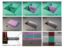 | Fig. 5. Schematic procedure for fabricating the nanostripes by using focused ion beam and scanning electron microscopy (FIB-SEM) dual beam system (Helios NanoLab 600i, FEI) equipped with a Gas Injection System (GIS), and Omniprobe 200 + micro-manipulator. Images are taken from Ref. [26]. |
Recently, many theoretical studies have demonstrated the plausibility of hosting and manipulating individual skyrmions in helimagnetic nanostripes.[9– 11] In such a scheme, the nanostripe is encoded with a chain of individual skyrmions that is under precise control by spin polarized current pulses. According to the theoretical results, a skyrmion can be transferred from the domain-wall pair in junction geometry, and a strategy for the design of skyrmion-based race-track memory has also been developed. By contrast, the experimental process is slow, mainly due to the difficulty of sample fabrication and the resolution limits of measurement tools. Until very recently, it remained unclear whether a skyrmion could really exist in such a confined geometry and how stable it would be. In the following chapters, the first experimental demonstration of individual skyrmions in a nanostripe is introduced.
As discussed in Section 2, Lorentz TEM possesses high resolution, so that it is very suitable to observe the spin textures in helical magnets. Lorentz TEM uses the Fresnel method or out-of-focus conditions to obtain the nanometer-scale magnetic structures. In principle, this technique should be adaptable to observe the magnetic state in ultra-narrow stripes. However, the sharp interface between sample and vacuum would lead to strong Fresnel fringes and give rise to artificial magnetic contrast around the edge.[16] As a result, the real spin configurations around the edge are severely smeared in such small-size samples (Fig. 6).
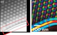 | Fig. 6. Lorentz TEM images and the constructed magnetic components around the edge. (a) The original image: The edge region is marked by the red rectangular. (b) The constructed in-plane magnetic components: a stripe domain with the width above 100 nm is marked by the red arrow, which is the artificial magnetic contrast due to the edge Fresnel fringes. Images are taken from Ref. [16]. |
Fresnel fringes show up along edges when we look at something out of focus using coherent illumination. These strong Fresnel fringes can be significantly reduced by coating the edge with a metallic layer. In transmission electron microscopy, Fresnel contrast occurs if the observed region in which the projected electromagnetic potentials — mean inner potential or magnetic potential or thickness — changes abruptly and is imaged under out-of-focus conditions.[20] The Fresnel fringe contrast is often seen at the edge of an object imaged out-of-focus. For magnetic characterization, the Fresnel imaging technique, as discussed in chapter 2, enables direct observation of magnetic structure, e.g. domain wall, provided that the thickness variation or projected electrostatic potentials are negligibly small as compared with the magnetic induction contributions.[21] However, at specimen edges, variation in Fresnel fringes due to the abrupt change in thickness overshadows the contrast change due to magnetic potential. This makes the analysis of magnetic information at the edge extremely difficult.
The use of amorphous PtCx adjacent to the edge of FeGe greatly reduces the effect of Fresnel fringes at the specimen edges due to the much-reduced variation in thickness, as opposed to the case of vacuum-edge. A direct comparison of Fresnel fringes at FeGe/PtCx and FeGe/vacuum interfaces is illustrated in Fig. 7. For this FeGe nanostripe, the PtCx layers were first coated on two sides of the stripe, and the right side PtCx layer fell off by chance. This enables us to directly compare the influence of the Fresnel fringes at the two FeGe/PtCx and FeGe/vacuum interfaces. Figures 7(a), 7(b), and 7(c) show the TEM images of the two interfaces under in-, over- and under-focus conditions, respectively. The yielded magnetic components are shown in Fig. 7(d), where the significantly reduced Fresnel effect at the FeGe/PtCx interface is clearly observed. It is therefore possible to investigate the magnetic helix and skyrmion states in a geometrically confined nanostructure by real-space Lorentz microscopy observation.
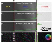 | Fig. 7. Comparison of Fresnel fringes at PtCx/FeGe and FeGe/vacuum interfaces: (a), in-focus case; (b), over-focus case with the defocus value 96 μ m; (c), under-focus case with the same defocus value 96 μ m. It is clearly shown that the range of Fresnel fringes extends above ∼ 100 nm at the FeGe/vacuum interface in the over-focus or under-focus conditions, while it is below ∼ 50 nm at the PtCx/FeGe interface [(b) and (c)]. Moreover, compared with the FeGe/vacuum interface, the strength of Fresnel fringes at the FeGe/PtCx interface is also significantly weakened. This advance enables the Lorentz TEM to directly image the edge state with less influence by the Fresnel fringes. (d) The artificial in-plane magnetic components constructed by the TIE analysis based on the image of panels (a)– (c). The significantly reduced Fresnel effect at the FeGe/PtCx interface is clearly observed. The red dotted lines indicate the position of the FeGe/PtCx and FeGe/vacuum interfaces. For clarity, the corresponding strength of Lorentz TEM images under different focus conditions is plotted as green lines. The white arrows in panel (d) represent the direction of lateral magnetization. Images are taken from Ref. [26]. |
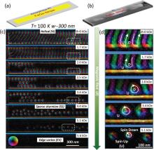
Now that we have reviewed the current solutions of the issues of sample fabrication and edge-induced Fresnel fringes, in this section, we address the experimental results on the formation and dynamics of skyrmions in FeGe nanostripes. FeGe exhibits a paramagnetic-to-helimagnetic transition at Curie temperature Tc∼ 280 K under zero magnetic field. Skyrmion states with crystal form survive only in a tiny temperature-field pocket near Tc in FeGe bulk since thermal fluctuation is required to stabilize it. The skyrmion crystal possesses a fixed lattice constant as∼ 81 nm, which is determined only by the ratio of Dzyaloshinskii– Moriya (DM) interaction over ferromagnetic exchange (FM) exchange interaction energy and is essentially independent of the sample size. Such a long period, as along with the high transition temperature, is favorable for experimental operations. Recent experiments show that reduced dimensionality stabilizes the skyrmion phase, significantly extending its range in both temperature and magnetic field. For example, for a 70-nm thick FeGe film, skyrmion states have been extended to 200 K. These properties include the T– B phase diagram, and the thickness dependence of the stabilization of skyrmions reflects the common features of helimagnets regardless of whether they are metals, semiconductors or insulators. A representative schematic and real TEM image of the sample are shown in Figs. 8(a) and 8(b), respectively. This stripe has a ∼ 90 nm thickness, and ∼ 300 nm width. The surrounding gray part is the amorphous Pt deposited by electron beam. The coating Pt layer significantly reduces the edge fringe ring, as mentioned in subsection 4.1. The external magnetic field B is applied perpendicular to the stripe plane.
Typical Lorentz TEM data for increasing applied fields after zero field cooling from room temperature to 100 K are summarized in Figs. 8(c) and 8(d). Each row is composed of the real-space image and an enlarged section of the same image. In zero field, the Lorentz TEM image reveals a helical ground state with a period of 70 nm, as previously reported.[17] The helical state orients predominantly with its wave vector parallel to the long edge of the stripe. Such sample-shape dependent orientation of the helical state is different from neutron diffraction findings on the bulk single crystal and Lorentz TEM observation on thin plates of FeGe samples, in which the wave vector is fixed along certain crystal axis determined by weak crystal anisotropy.[17] A similar phenomenon has been observed in the conventional stripe domain of micro-sized Ni wires with large perpendicular anisotropy, where theoretical analysis identified that the stripe domain prefers to be either perpendicular or exactly parallel to the edge of the sample, with all other orientations being energetically less favorable due to the effect of stray field.[27, 28] In fact, this theoretical result may also be suitable for the current case, in which we observed a helical sate with its wave vector perpendicular to the long edge of the stripe in other samples.
The helix state is distorted in the edge with the in-plane spin orientation parallel to the edge, forming a “ half-disk” domain (Fig. 8(d)B = 0 kOe). When a weak external magnetic field is applied normal to the stripe plane, the Zeeman effect enforces an increase of the up-spins. In an ideal two dimensional film without defects, this is accomplished by splitting the stripe into pieces of bimeron with up-spins in the linked region.[29] By contrast, in the nanostripe, the increased up-spins occur by extending the region of up-spins among the edge and two merons, as marked by “ U” in the black-colored region. This black contrast means the lateral magnetization is nearly zero, yielding spins normal to the nanostripe plane. But Lorentz TEM cannot specify the direction the magnetization points. Instead, this is inferred from comparison with the Lorentz TEM image at high field, where a larger upward component along the direction of external field appears. In this manner, the spins in region U should point upward, while the spins in region D should points downward, which is also in accord with the well-established model that the direction of spins in the core of a skyrmion is antiparallel to the orientation of the magnetic field. According to published numerical calculations, the edge spins cannot point strictly normal to the stripe plane even at highest field, due to the requirement of global minimal energy.[30, 31] Thus, this extension of region “ U” will gradually decouple the bulk stripe domain from the edge with increasing magnetic field, yielding a clear edge state with its in-plane spins parallel to the edge and a reversed meron with a clockwise rotation direction and down-spins in the core, similar to the skyrmion (B = 1.7 kOe).
Once the separation between edge state and meron is completed, the magnetization dynamics in the meron are similar with that in two-dimensional films, where increasing magnetic field leads to the formation of skyrmions via shrinking the bimeron. At the same time, the magnetization swirls around the edge form a complete big edge vortex. This leads to an effective repulsive force pushing the skyrmions away from the edge.[8] As the magnetic field is further increased, a sparse skyrmion chain is formed along the nanostripe due to a balance between skyrmion-skyrmion and skyrmion-edge repulsion. At higher field, this skyrmion chain transforms into a field-polarized ferromagnetic state, rendering no magnetic contrast in the lateral components, while the edge vortex still persists.
At elevated temperature, the distorted skyrmion chain persists. Above a threshold temperature T∼ 190 K, increasing temperature will increase the number of skyrmions (Fig. 9(a)). In this case, a skyrmion nucleation and formation mechanism similar to 2D films is observed, where the helical state is first split into pieces of bimeron, then turns into packed skyrmions with the increase of magnetic field. A slight difference lies in the breakup of the stripe domain that occurs preferentially in the edge.[32] On the basis of Lorentz TEM images, we constructed the common T-B phase diagram by contour mapping of normalized skyrmion density 

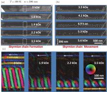 | Fig. 10. Variations of spin texture with magnetic field in 396-nm FeGe nanostripe at T = 100 K. (a) and (b) Magnetic-field dependence of the spin texture — the crystal boundaries in the right are marked by white dotted lines. (c) The region marked by the dotted white rectangle in corresponding panels (a) and (b) enlarged. The small white arrows stand for the in-plane magnetization direction at each point. The thick white arrows are plotted to guide the eyes. |
The unexpected emergence of skyrmions at low temperature at T = 100 K can be well understood by investigating the magnetization dynamics of a nanostripe with wide width. A typical variation of spin texture with magnetic field in 396-nm nanostripe is shown in Fig. 10. The corresponding part of some typical images is also shown enlarged. Compared with a 300-nm nanostripe, the nanostripe shows orthogonal Q helical ground states with the co-existence of helical states with Q | | edge or Q⊥ edge. Such experimental observations reinforce the above-mentioned conclusion that both sample-shape dependent helical states are energetically favorable. Unlike the distorted edge spin configurations of a helical state with Q | | edge, a complete edge state is spontaneously isolated from the helical state with Q⊥ edge.
When the magnetic field is switched on, the magnetization process is more complex than that in 300-nm nanostripe, involving the preferential formation of skyrmions in the corner and crystal boundary. In spite of the detail, the most striking feature of formation of skyrmion chain still persists. At B ∼ 1.6 kOe, the orthogonal Q helical states show a remarkable difference. The helical state with Q⊥ edge becomes less visible, while the helical state with Q ∥ edge is decoupled from the edge spins, yielding compressed bimerons with the edge state. With further increasing magnetic field, the helical state with Q⊥ edge disappears, while the compressed bimerons shrink (B ∼ 2.2 kOe) and eventually organize as dense skyrmion chains pinned by the edges together with a small number of skyrmion clusters (B ∼ 3.5 kOe) around the corner. This field-driven evolution of helical state with Q | | edge is essentially consistent with that of the 300-nm nanostripe with a prominent property that the skyrmion chain is preferentially organized along the edge. By contrast, the evolution of helical state with Q⊥ edge is similar with that in 2D plates at low temperature, [17] where the helical state shrinks without forming skyrmions. Taken together, they lead to the conclusion that the skyrmion chain along the edge forms only if the helical ground state has its wave vector Q | | edge. Meanwhile, the current case is distinct from the previously reported preferential formation of skyrmions near the sample edge in 2D plates of FeGe, found by using Lorentz TEM images.[17] The samples, fabricated by traditional argon-ion thinning methods, have an inhomogeneous thickness with a thin region at the edge, which creates skyrmion phase around the thin edge mainly due to the stabilizing effect of reduced thickness. Once the separation of skyrmions and edge state is completed, the collective move of skyrmions into the center of the nanostripe is also observed in the wider nanostripe with the increase of magnetic field, wherein the number of skyrmions is unchanged in a wide interval of magnetic field.
 | Fig. 11. Sample width dependence of the skyrmion phase diagram in the plane of temperature and magnetic field. Panels (a)– (c) are all composed of three parts: sparse skyrmion chains in the FeGe stripe with varied width at low temperature T = 100 K obtained as magnetic field is changed; packed skyrmions in corresponding samples at high temperature T = 220 K; sample width dependence of the skyrmion phase diagram in the plane of temperature and magnetic field. |
This edge-mediated skyrmion chain is independent of sample width (Fig. 11). More importantly, as the width of the stripe decreases to slightly bigger than the single skyrmion size, simple geometric analysis identifies that at most one skyrmion can be filled into the stripe in the transverse direction. Thus, the packed skyrmions at high temperature are the same as the skyrmion arrangements at low temperature. So a perfect single skyrmion chain is formed throughout the whole temperature region (Fig. 11(c)). This single skyrmion chain is the foundation of the concept of skyrmion-based racetrack memory, so the experimental observation gives strong support to the device concept.
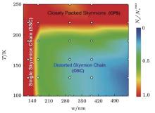 | Fig. 12. Sample width dependence of the skyrmion arrangement in the temperature (T)– width (w) diagram. The open dots are data points from the Lorentz TEM measurements. From these data, a colored map is constructed to show the normalized skyrmion density, defined as   |
Based on all the Lorentz TEM data on nanostripes with various widths measured at different temperatures, we constructed a full T– w phase diagram of the skyrmions in nanostripes (Fig. 12). While the maximum number 
In this work, the edge can be used to control skyrmions formation in confined geometries. At high temperatures, skyrmions tend to form a closely packed structure. This skyrmion arrangement is consistent with previous experimental results on the skyrmion crystal in the corresponding 3D or 2D FeGe compounds.[3, 17] In this case, a single skyrmion chain can be obtained by reducing the width of the nanostripe to the featured skyrmion size. More importantly, the single skyrmion chain persists even in much wider nanostripes at low temperatures. The skyrmions originate from the sample-shape dependent orientation of the helical state. The helix with distorted edge state evolves into skyrmions, while those without distorted edge state transfer into the ferromagnetic state directly. Taking the topological stability of skyrmions into account, it is commonly concluded that skyrmions cannot easily be destroyed and created from the single-twist magnetic structure, including helical and conical phase. By contrast, the confined effect gives rise to the distorted edges states, which show half-disk arrangements, indicating their multi-twist modulations. The results thus indicate that the creation of the skyrmion from the multi-twist magnetic state is much easier than that from single-twist magnetic state. These findings offer fundamental insight into the dynamical mechanism of the formation and evolution of skyrmions in a confined geometry, and might improve the viability of proposals for using skyrmions in magnetic nanostripes as the carriers of high-density information through edge- or defect-engineering.
In addition, the collective motion of the skyrmion chain is accompanied by a series of adjustments in the chain space and position. This motion is the direct result of skyrmion– skyrmion and skyrmion– edge repulsions. The presence of spin distortion around the edge is a fundamental property in geometry-confined nanostructures. This edge-mediated mechanism together with control of temperature and thickness could provide a powerful approach for tailoring the desired skyrmion properties in confined geometries.
| 1 |
|
| 2 |
|
| 3 |
|
| 4 |
|
| 5 |
|
| 6 |
|
| 7 |
|
| 8 |
|
| 9 |
|
| 10 |
|
| 11 |
|
| 12 |
|
| 13 |
|
| 14 |
|
| 15 |
|
| 16 |
|
| 17 |
|
| 18 |
|
| 19 |
|
| 20 |
|
| 21 |
|
| 22 |
|
| 23 |
|
| 24 |
|
| 25 |
|
| 26 |
|
| 27 |
|
| 28 |
|
| 29 |
|
| 30 |
|
| 31 |
|
| 32 |
|


