Key Laboratory of Wide Band-Gap Semiconductor Materials and Devices, School of Advanced Materials and Nanotechnology, Xidian University, Xi’an 710071, China
Key Laboratory of Wide Band-Gap Semiconductor Materials and Devices, School of Microelectronics, Xidian University, Xi’an 710071, China
*Project supported by the Program for National Natural Science Foundation of China (Grant Nos. 61404100 and 61306017).
Abstract
In this paper the trapping effects in Al2O3/In0.17Al0.83N/GaN MOS-HEMT (here, HEMT stands for high electron mobility transistor) are investigated by frequency-dependent capacitance and conductance analysis. The trap states are found at both the Al2O3/InAlN and InAlN/GaN interface. Trap states in InAlN/GaN heterostructure are determined to have mixed de-trapping mechanisms, emission, and tunneling. Part of the electrons captured in the trap states are likely to tunnel into the two-dimensional electron gas (2DEG) channel under serious band bending and stronger electric field peak caused by high Al content in the InAlN barrier, which explains the opposite voltage dependence of time constant and relation between the time constant and energy of the trap states.
III-nitride metal– oxide– semiconductor HEMTs (MOS-HEMTs) (here, HEMT stands for high electron mobility transistor) are highly preferable to the Schottky-gate HEMTs due to their ability to effectively suppress gate leakage current and enhance the breakdown voltage.[1– 3] However, trap states at the interface introduced by gate dielectrics cause reliability problems, such as drain saturation current decreasing and threshold voltage drifting. So it is required to study the trap states in Schottky AlGaN/GaN and AlGaN/GaN MOS-HEMTs.[4– 7] Recently, attention has shifted to trap states in high Al barrier AlGaN/GaN heterostructure.[8– 10] High Al content is an effective method to enhance the breakdown performance due to the wider band-gap and higher critical breakdown field, yet the immature material growth would introduce trap states into the surface, interface, or bulk material.[11] A comparison of the trap state between the two kinds of HEMTs reveals the inherent mechanism of the trapping/detrapping process. Meanwhile, lattice-matched InAlN/GaN, as another high Al barrier heterostructure, has always been a reasonable substitute for AlGaN/GaN HEMTs because its strong spontaneous polarization and strain-free in heterostructure are necessary qualities for high frequency and power electronics applications.[12– 14] However, the trap analysis of InAlN/GaN HEMT with high Al content is still a comparatively less explored area.
In this work, the trapping effect of a thin barrier In0.17Al0.83N/GaN lattice matched HEMT is investigated using frequency-dependent conductance measurements. To suppress the large off-state leakage current, a Al2O3 gate insulator grown by atomic layer deposition (ALD) is fabricated on the semiconductor interface. Three trap states are observed at two interfaces, which shows the complicity of the high-Al and gate-oxide of the interfaces of the GaN HEMT.
2. Experimental method
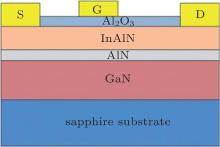
The InAlN/GaN heterostructure was grown on a sapphire substrate by the PMOCVD method at Xidian University.[15] The epitaxial layer shown in Fig. 1 contains a 12-nm lattice-matched In0.17Al0.83N barrier layer, a 1.2-nm AlN interlayer, and a 1.6-μ m GaN buffer layer. Hall effect measurements at room temperature show that the sheet carrier density is 1.7× 1013 cm− 2, the two-dimensional electron gas (2DEG) mobility is 1180 cm2/V· s, and the sheet resistance is 306 Ω /sq. The epitaxial layer was first fabricated by Cl2 plasma mesa isolation using reactive ion etching (RIE). Ohmic contacts consisting of Ti/Al/Ni/Au were annealed in N2 ambient at 830 ° C for 30 s at second step. The Ohmic contact resistance was confirmed to be 0.8 Ω · mm. Then, a 12-nm Al2O3 film was deposited at 300 ° C by the ALD method, which acts as a gate dielectric. Finally, Si2N3 was deposited on the whole active area as a passivation layer by the plasma enhanced chemical vapor deposition (PECVD) method.
Fig. 1. Cross-section of the Al2O3/InAlN/AlN/GaN MOS-HEMT.
3. Results and discussion
Figure 2 shows the variations of the representative capacitance– voltage (Cm− V) with swept voltage, which were obtained with a Keithley 4200SCS semiconductor analyzer at room temperature. Two kinds of capacitance dispersions appear as the frequency varies from 10 kHz to 1 MHz, one transition happens around − 5 V, which corresponds to the strong accumulation of 2DEG in the GaN channel, and the other happens around − 1 V, which corresponds to the capacitance transition of the MOS structure, indicating that the trap states exist at both the InAlN/GaN interface and the Al2O3/InAlN interface.
Fig. 2.Cm– V characteristics at given frequencies.
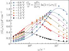
In order to analyze the dynamic capacitance dispersion, the variations of parallel trap conductance with frequency at different voltages are measured. The trap conductance Gsurf/ω is calculated based on measured conductance Gm and capacitance Cm (the measurement circuit is shown in the inset of Fig. 2) through the following relation:
where ω = 2π f is the radial frequency and C0 = 50 pF represents the static-state capacitance of the MOS-HEMT. The voltage range is set to be − 1.4 V– 0.8 V according to the capacitance dispersion region in Fig. 2.
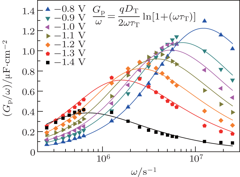
Figure 3 shows the trap conductance dispersions with the devices biased in the accumulation region. Given that the 2DEG channel is saturated under high voltage and no electrons are captured at the InAlN/GaN interface, only the traps at the Al2O3/InAlN interface can be released and detected by the ac signal. The density of trap states (DT) and the time constant (τ T) can be evaluated by fitting the experimental Gp/ω to a function of ω according to equation in the inset of Fig. 3. The measured data (symbols) and fitted curves (lines) are obtained to be in good agreement with each other under the assumption of a continuum of trap levels.
Fig. 3. Experimental (symbols) and fitting (lines) Gp/ω versus radial frequency near the accumulation region. The inset shows the equation that is used to evaluate the trap density and time constant.
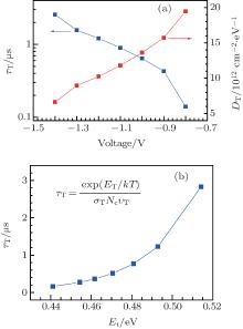
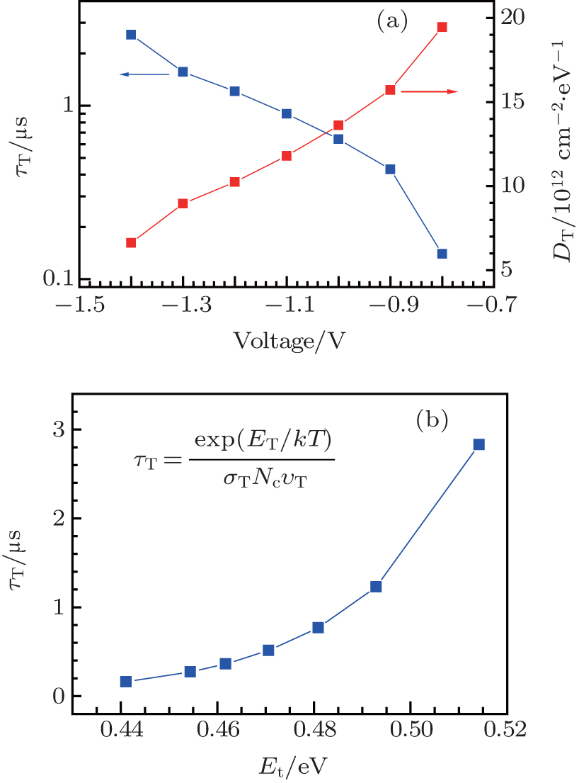
Figure 4(a) shows that the time constant of trap at Al2O3/InAlN interface decreases exponentially from 2.83 μ s to 0.16 μ s with the increase of voltage. As the voltage increases, the Fermi level rises, so that more fast (shallow) traps can be detected by the measurement. The trap density at Al2O3/InAlN interface changes with τ T according to a linear law from 0.60 × 10¹³ eV− 1· cm− 2 to 1.89 × 10¹³ eV− 1· cm− 2. Et (equals Ec− Esurf) representing the trap level below conduction band (CB) is estimated to be within a range from 0.44 eV to 0.51 eV according to the equation in the inset of Fig. 4(b). Room temperature T = 300 K, capture cross section σ T = 4 × 10− 13 cm− 2, effective density of states in the conduction band Nc = 2.2 × 10¹⁸ T3/2· cm− 3, and average thermal velocity of the carriers υ T = 2.6 × 107 cm/s for GaN are used for the calculation.[4] There are no deep traps compared with the results from other AlGaN/GaN articles in which Et is up to 0.5 eV. This is partially due to the Al2O3/InAlN interface (no GaN cap layer) without Ga, because the easy formation of Ga– O bonds gives rise to massive interface traps.[16]
Fig. 4. (a) Time constant of trap states as a function of gate voltages. (b) Trap state density as a function of energy Et.
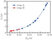
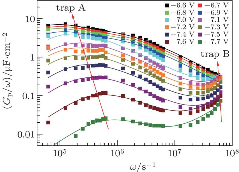
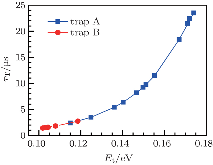
Figure 5 gives the trap conductance dispersions near the threshold voltage. The trap states at InAlN/GaN interface are mainly responsible for the conductance dispersion as the heterostructure is charged by the capacitance transition. We assume that part of the density of trap states is introduced by the subsequent high temperature annealing process due to the lack of a GaN cap layer.[10] Meanwhile, in Fig. 6, the time constants of the two kinds of traps show opposite features. In other reports involving with the trap states of low Al content structures, time constant decreases with increasing voltage. However, in this work, where the Al content is up to 83% in the InAlN barrier layer, the time constant of trap B decreases from 2.8 μ s to 1.4 μ s as the voltage increases, while the time constant of trap A increases from 2.37 μ s to 22.4 μ s. We believe that there are mixed de-trapping mechanisms in trap A and that the electron tunneling is the main reason for the dependence of the time constant on the abnormal voltage.
Fig. 6. Time constants of trap states as a function of gate voltage in both trap states.
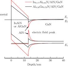
The electron tunneling effect can be explained by using the one-dimensional simulation of the band diagram and polarization electric field shown in Fig. 7, which is derived from the self-consistent solutions of Schrö dinger and Poisson’ s equations. Another structure with 12-nm Al0.30Ga0.70N barrier is also simulated for comparison. Commonly, the electron emission from trap states to the conduction band level is considered to be the cause of the dynamic capacitance dispersion. As voltage increases, EF at interface approaches to CB and the shallower trap states exhibit decreased emission time τ E (equal to trap time constant).[9]
Fig. 7. Simulated band diagram and polarization electric field of In0.17Al0.83N/AlN/GaN and Al0.30Ga0.70N/AlN/GaN structures.
However, in a high Al content barrier, more serious band bending and stronger electric field peak exist at the interface and barrier, so electrons captured in trap states could possibly tunnel into the 2DEG channel, making the de-trapping process different. The time constant is mainly determined by the tunneling of electrons other than the emission to CB.[9] Thus, the rising of voltage reduces the electric field in the barrier layer, resulting in a longer tunneling time, which leads to an increased time constant of trap A. Moreover, the τ T− Et relations of the two traps show a strong correlation in Fig. 8. The Et of trap B, varying from 0.441 eV to 0.458 eV, is just below the Et of trap A. Since trap B is closer to the conduction band than trap A, the de-trapping process of trap B is possibly caused by voltage changing, and the electrons in the deeper trap A may be de-trapped by the tunneling effect, which proves to be a different de-trapping mechanism of two kinds of traps.
Fig. 8. Time constants as a function of energy in both trap states.
4. Conclusions
In this paper, we report on a detailed analysis of trap states in ALD Al2O3/In0.17Al0.83N/GaN MOS-HEMT. Trap densities, trap energies, and time constants are determined by frequency-dependent capacitance and conductance measurements. The trap states are found at both Al2O3/InAlN and InAlN/GaN interfaces, and the trap states in InAlN/GaN heterostructure are determined to have two different de-trapping mechanisms. The electrons captured in the trap states are likely to tunnel into the 2DEG channel under serious band bending and stronger electric field peak caused by high Al content in the In0.17Al0.83N barrier, which explains the opposite voltage dependence of the time constant. Furthermore, strong correlations in τ T− Et of both traps can also be explained as the transition from normal electron emission to electron tunneling of the de-trapping process. More experimental data that can reveal the inherent mechanism of the traps states process are necessary for further research.
FreedsmanJ J, KuboT and EgawaT2011Appl. Phys. Lett. 99033504DOI:10.1063/1.3614556[Cited within:1]
6
KordosP, StoklasR, GregusovaD, GaziS and NovakJ2010Appl. Phys. Lett. 96013505DOI:10.1063/1.3275754[Cited within:1]
7
MaX H, ZhuJ J, LiaoX Y, YueT, ChenW W and HaoY2013Appl. Phys. Lett. 103033510DOI:10.1063/1.4813912[Cited within:1]
8
ZhangK, XueJ S, CaoM, YangL, ChenY, ZhangJ and HaoY2013Appl. Phys. Lett. 113174503[Cited within:1]
9
ZhuJ J, MaX H, HouB, ChenW W and HaoY2013AIP Adv. 4037108DOI:10.1063/1.4869020[Cited within:2]
10
ZhangP, ZhaoS L, XueJ S, ZhangK, MaX H, ZhangJ C and HaoY2014Chin. Phys. Lett. 31037302DOI:10.1088/0256-307X/31/3/037302[Cited within:2]
11
ZhaoS L, ZhangK, HaW, ChenY H, ZhangP, ZhangJ C, MaX H and HaoY2013Appl. Phys. Lett. 103212106DOI:10.1063/1.4832482[Cited within:1]
12
MedjdoubF, CarlinJ F, GonschorekM, FeltinE, PyM A, DucatteauD, GaquiereC, Grand jeanN and KohnE2006IEDM Electron Devices MeetingDecember 10–13, 2006San Francisco, CA, USA129134DOI:10.1109/IEDM.2012.6479034[Cited within:1]
13
XueJ S, ZhangJ C, HouY W, ZhouH, ZhangJ F and HaoY2012Appl. Phys. Lett. 100013507DOI:10.1063/1.3675453[Cited within:1]
... 3] However, trap states at the interface introduced by gate dielectrics cause reliability problems, such as drain saturation current decreasing and threshold voltage drifting ...
2
2010
0.0
0.0
... [4#cod#x2013 ...
... [4] There are no deep traps compared with the results from other AlGaN/GaN articles in which Et is up to 0 ...
1
2011
0.0
0.0
1
2010
0.0
0.0
1
2013
0.0
0.0
... 7] Recently, attention has shifted to trap states in high Al barrier AlGaN/GaN heterostructure ...
1
2013
0.0
0.0
... [8#cod#x2013 ...
2
2013
0.0
0.0
... [9] ...
... [9] Thus, the rising of voltage reduces the electric field in the barrier layer, resulting in a longer tunneling time, which leads to an increased time constant of trap A ...
2
2014
0.0
0.0
... 10] High Al content is an effective method to enhance the breakdown performance due to the wider band-gap and higher critical breakdown field, yet the immature material growth would introduce trap states into the surface, interface, or bulk material ...
... [10] Meanwhile, in Fig ...
1
2013
0.0
0.0
... [11] A comparison of the trap state between the two kinds of HEMTs reveals the inherent mechanism of the trapping/detrapping process ...
1
2006
0.0
0.0
... [12#cod#x2013 ...
1
2012
0.0
0.0
1
2011
0.0
0.0
... 14] However, the trap analysis of InAlN/GaN HEMT with high Al content is still a comparatively less explored area ...
1
2011
0.0
0.0
... [15] The epitaxial layer shown in Fig ...
1
2007
0.0
0.0
... [16] ...
Investigation of trap states in Al2O3 InAlN/GaN metal–oxide–semiconductor high-electron-mobility transistors


 , Zhao Sheng-Lei