


Nature of the band gap of halide perovskites ABX3 ( A = CH3NH3, Cs; B = Sn, Pb; X = Cl, Br, I): First-principles calculations*
[Yuan Yea) , Xu Runa)  , Xu Hai-Tao
a) , Hong Fengb) , Xu Feib) , Wang Lin-Juna) ]
, Xu Hai-Tao|
|


†Corresponding author. E-mail: runxu@staff.shu.edu.cn
*Project supported by the National Natural Science Foundation of China (Grant No. 11375112).
The electronic structures of cubic structure of ABX3( A=CH3NH3, Cs; B=Sn, Pb; X=Cl, Br, I) are analyzed by density functional theory using the Perdew–Burke–Ernzerhof exchange–correlation functional and using the Heyd–Scuseria–Ernzerhof hybrid functional. The valence band maximum (VBM) is found to be made up by an antibonding hybridization of B s and X p states, whereas bands made up by the π antibonding of B p and X p states dominates the conduction band minimum (CBM). The changes of VBM, CBM, and band gap with ion B and X are then systematically summarized. The natural band offsets of ABX3 are partly given. We also found for all the ABX3 perovskite materials in this study, the bandgap increases with an increasing lattice parameter. This phenomenon has good consistency with the experimental results.
Perovskites are of great interest in materials science because of their electric, magnetic, piezoelectric, optical, catalytic, and magnetoresistive properties.[1, 2] The hybrid organic-inorganic halide perovskite materials have recently revolutionized the photovoltaic field.[3– 6] The search for this class of solar cell materials amazed researchers and industry community.
Theoretically, a number of first-principles calculations for ABX3 (A= CH3NH3, Cs; B= Sn, Pb; X= Cl, Br, I) have been reported in recent years. However, some questions remain to be addressed regarding the electric properties of these materials. For example, the electronic structures of valence-band maximum (VBM) and conduction-band minimum (CBM) are still controversial. For the VBM firstly, most research points out that the X p and B s electrons contribute majorly. For instance, Umebayashi et al. in 2003, [7] found that the top of the valence band is found to consist mainly of the σ antibonding states of Pb s and I p orbitals for CH3NH3PbI3 and (C4H9NH3)2PbI4. Federico et al.[8] also proved that the VBM is formed in an antibonding Pb s– I p* combination for (NH4)PbI3 and (CH3NH3)PbI3. Li et al.[9] demonstrated that the VBM is an antibonding state of B s– X p* coupling for ABX3 (A= Cs, CH3NH3, NH2CHNH2; B= Sn, Pb; X= Cl, Br, I) type compounds in the cubic phase. Although most researchers emphasized the VBM featured by the antibonding states of B s and X p orbitals, some researchers like Ghebouli et al.[10] also considered the contribution of B p state to VBM. They found that the upper valence band reflects the p electronic character mainly, due to the Cl p, Pb p, and small contribution to Pb s for CsPbCl3.
The nature of CBM seems to be more controversial as compared with that of VBM. The conduction-band minimum is characterized by a non-bonding hybrid state of the B p and the X p orbitals in the study of Park et al.[11] Umebayashi et al.[7] pointed out that the bottom of the conduction band is composed primarily of the σ antibonding states of Pb p and I s orbitals for CH3NH3PbI3 and (C4H9NH3)2PbI4. The CBM of the cubic perovskites CsPbM3 (M= Cl, Br, I) is mainly due to the Pb p state and Cs d state.[12] Li et al.[9] thought that the CBM is a non-bonding state with B p characters.
Up to now, there has been hardly any systematic study on the nature of VBM and CBM of these ABX3 perovskite materials. In this work, we calculated the band structures and density of states of ABX3 (A= CH3NH3, Cs; B= Sn, Pb; X= Cl, Br, I) by both the Perdew– Burke– Ernzerhof (PBE) exchange– correlation functional[13] and using the Heyd– Scuseria– Ernzerhof (HSE) hybrid functional.[14] In the results of both PBE and HSE, the top of valence band is found to be made up by an antibonding linear combination of B s states and X p states, whereas the bands made up by the π antibonding states of B p and X p dominate the bottom of conduction band. The strong antibonding B s– X p state may be more delocalized than the X p alone, likely leading to a small hole effective mass and thus large mobility of the hole of the perovskite solar cell.[15] Using the above conclusion, we systematically investigate the variation of VBM and CBM for ABX3 (A= CH3NH3, Cs; B= Sn, Pb; X = Cl, Br, I) series. Based on the above discussion, the changes of VBM, CBM, and the band gap with B and X ions are systematically summarized. The increase of the band gap of ABX3 with the lattice parameter, in contrast to most general semiconductors, is also reported, which is in good accord with experimental results.[16]
We investigate the electronic and structural properties of ABX3 (A= CH3NH3, Cs; B= Sn, Pb; X= Cl, Br, I) using both the Perdew– Burke– Ernzerhof parameterization of the generalized gradient approximation and the screened hybrid functional of HSE non-local approximation, in which a portion of Hartree– Fock (HF) exchange is mixed with GGA exchange and correlation.[17] The advantage of the HSE method is a balance between the efficiency and accuracy. In addition, the HSE can be more accurate in describing the localized state due to the partial elimination of self-interaction error of semi-local functional, and it is very accurate to calculate the optical band gap using the HSE method.
We performed calculations based on the density functional theory as implemented in the code (Vienna ab initio simulation package) VASP.[18] The electron– ion interaction is described by PBE potential. The valance wave functions are expanded in a plane-wave basis with a cutoff energy of 350 eV. All the calculations were performed using 5-atom cubic cells and a 10 × 10 × 10 grid was used for the k-point sampling of Brillouin zone. All the atoms were relaxed to minimize the Feynman– Hellmann forces to below 0.02 eV/Å . The calculations were performed by potentials with both the PBE– GGA form and the HSE hybrid functional form. For the HSE method, two parameters are introduced in the hybrid functionals. A fraction β of non-local exact exchange is mixed to the GGA exchange. Hence, the exchange energy is given by
 |
The correlation potential is taken from the GGA absolutely. It turns out that the exact exchange contribution β = 0.25 is considered to be optimal for both lattice constants and the band gap in ABX3. For the other parameter, screening length, the value of around 0.2 Å − 1 is adopted.
As representative of ABX3(A= Cs, CH3NH3; B= Sn, Pb; X= Cl, Br, I), CsPbI3 and CH3NH3PbI3 crystallizes in the perovskite structure, which are respectively shown in Figs. 1(a) and 1(b). The structure belongs to the cubic space groups 221 pm3m. B is a metal bonded to six X anions, and BX6 octahedra are corner-connected to form a three-dimensional framework. The band structures of CsPbI3 and CH3NH3PbI3 calculated by the HSE method are depicted in Fig. 1(c). The results show that the minima of conduction bands (CBs) and the maxima of valence bands (VBs) are at R(0.5, 0.5, 0.5) symmetry point in the Brillouin zone. Hence, these ABX3 perovskites in cubic phase have fundamental direct band-gap nature at R symmetry point.
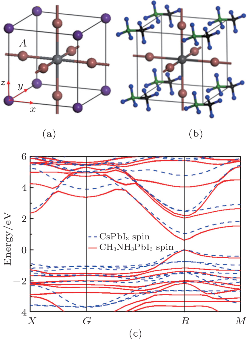 | Fig. 1. The crystal structure of (a) CsPbI3 and (b) CH3NH3PbI3. (c) The corresponding energy band structure obtained using HSE method including the spin orbit coupling, where the energy of VBM is set at zero. |
The lattice constants and band gaps of CsBX3 and CH3NH3BX3 obtained by using both PBE and HSE methods are listed in Table 1. The calculated lattice constants by both PBE and HSE functional are in good agreement with others’ values.[9] For both ASnX3 and APbX3 (A= Cs and CH3NH3), the lattice constant increases from Cl to I. A similar trend can be found from Sn serials to the corresponding Pb serials with a larger lattice constant. The reason for this is simply due to the larger atom of Pb or I atom than that of Sn atom or Cl atom. From Table 1, we can also notice that the band gaps of ASnX3 and APbX3 decrease from Cl to I, and the band gaps of lead compounds is larger than that of the corresponding tin compounds. The reason for this is given below according to the explanation of the origin of VBM and CBM. The band gap calculated by the HSE methods without considering the spin orbit coupling (SOC) gives a better agreement with the experimental results. However, the SOC effect is important to the Pb and Sn materials as indicated by Table 1, and it leads to the lowering of CBM due to the splitting of p1/2 and p3/2 state. The SOC splitting energy is about 0.34 eV and 1.11 eV for Sn and Pb, respectively. Hence, the HSE method with the SOC effect still underestimates the band gap of materials of this kind. The van der Waals interactions are not considered in both PBE and HSE methods, leading to a little larger lattice constants and slightly wider bandgaps. All these results are well consistent with Umari et al.’ s results.[19]
| Table 1. Lattice constants and energy gap of ABX3 using both PBE and HSE method. |
The total density of states and the atom projected density of states for CsPbCl3 calculated using HSE method is shown in Fig. 2. All twelve ABX3 compounds have a similar energy distribution of the eigenstates. The semi core state of Cs p states forms a narrow band located at a deep energy of − 8 eV, and have almost no contribution to the VBM and CBM. The Pb s and Cl p states are clearly visible at the same position from − 9 to − 6.5 eV and − 2 to 0 eV, respectively, indicating a hybrid state of Pb s and Cl p state. The VBM (− 2 to 0 eV) is clearly made up of the σ antibonding of the Pb s and Cl p hybrid state. The contribution of Pb p to VBM is also discernible but fairly small. The strong antibonding Pb s– Cl p state may be more delocalized than the Cl p alone, likely resulting in the small hole effective mass and thus large mobility of the hole of the perovskite solar cell.[14]
 | Fig. 2. Partial and total DOS of CsPbCl3 calculated using HSE method without SOC: (a) total DOS of CsPbCl3; (b) partial DOS for Cs atom; (c) partial DOS for Pb atom; (d) partial DOS for Cl atom. |
As for the CBM, a hybrid state between Pb p and Cl p can be observed in the energy range between 3 and 7 eV (see Fig. 2). The contribution to the energy of around 3 eV is from the Pb p state mixed slightly with the Cl pz and Cl py state at the A position as shown in Fig. 1(a), i.e., the π antibonding state of Pb p and Cl p state. The corresponding π bonding state of Cl p state with weak hybridization of Pb p state is located at about − 3.2 eV. In contrast, the σ interaction of px state of Cl at the A position with the Pb p state indicates a much stronger hybridization. The peak at about − 4.0 eV corresponds to this σ bonding of Cl p with hybridization of the Pb p state. Except for the σ and π bonding and antibonding state, the p state of Cl also has a clear non-bonding state corresponding to the highest peak of I p orbits at − 2.3 eV.
The DOS in Fig. 3 represents the aligned total density of states of CsSnX3 and CsPbCl3 calculated by using the HSE method. The zero position is aligned with the vacuum energy using the slab model. To position the VBM relative to the vacuum energy level, a common reference energy should be used for both the bulk and slab calculation. Here, the Cs core potential in the middle of atom layers of the slab model is aligned with that of the same atom in the bulk calculation. It is worthwhile noticing that a non-polar (100) surface ending with CsI is chosen to minimize the surface orientation and reconstruction effect on the position of VBM.
It is observed in Fig. 3 that different halogens change the absolute positions of both the CBM and VBM. We can find that both the VBMs of CsSnCl3 and CsSnI3 are lower than CsSnBr3. The CBMs of CsSnX3 are monotonically increased from CsSnI3 to CsSnBr3 to CsSnCl3. The change in magnitude of CBM is larger than VBM, leading to the overall decrease of the energy band gap. CsPbX3 and CH3NH3BX3 have similar trends.
 | Fig. 3. The total DOS of (a) CsPbCl3, (b) CsSnCl3, (c) CsSnBr3, and (d) CsSnI3 calculated by using the HSE method without SOC. The zero position of the horizontal ordinate means the position of vacuum energy. |
To further explain this trend of the band gap for ABX3, a schematic molecular orbital diagram of cubic CsSnCl3 and CsSnI3 is shown in Fig. 4. The atomic orbital energies of component elements of Sn, Cl, and I for CsSnX3 are shown in Fig. 4. The atomic orbital energy of Cl p is clearly lower than the energy of I p. The Cl p and I p orbitals interact with Sn s orbits, leading to the bonding orbitals of Sn s– Cl p and Sn s– I p, and the antibonding orbitals of Sn s– Cl p* and Sn s– I p* . This antibonding hybrid state constructs the VBM. The Sn p orbital also has a covalent interaction with Cl p and I p, leading to the bonding orbitals of Sn p– X p, and antibonding orbitals of Sn p– X p* . It should be noted that this interaction of Sn p and X p state contains both the π and σ bonding state of Sn p– X p. Only the π antibonding of Sn p– X p* contributes to the CBM.
 | Fig. 4. Energy level of CBM and VBM of CsSnCl3 and CsSnI3. |
As mentioned previously, the CBMs of CsSnX3 are monotonically decreased from Cl to Br, and then to I. The reason can be explained as follows. Since the Sn– X covalent interaction becomes stronger from I to Br to Cl due to the decrease of the length of Sn– X bond from Cl to Br to I, and the hybridization pulls the antibonding states up, and thus the state of Sn p– X p* goes up from I to Br to Cl. This leads to the increase of the CBMs of CsSnX3 from I to Br to Cl. As for the VBM, the antibonding of Sn s– X p* that contributes to the VBM should also be pulled up, and the magnitude of pulling up is increased from I to Br to Cl. However, the original energy level is decreased from I p, to Br p, and then Cl p, so it results in a complicated case that the VBM of CsSnBr3 is higher than CsSnCl3 and lower than CsSnI3. Similar trends are also found from CH3NH3SnCl3 to CH3NH3SnI3, and the reason for this is also identical.
The DOS in Fig. 3 also shows the aligned total density of states of CsPbCl3, and CsSnCl3. It is observed that the VBM of CsPbCl3 is lower than CsSnCl3, and the CBM of CsPbCl3 is higher than CsSnCl3, leading to a larger band gap of CsPbCl3. The higher VBM of CsSnCl3 is due to the stronger Sn s– Cl p* antibonding interaction than that of Pb s– Cl p* because of a small bond length of Sn– Cl. As for the CBM, the Pb p– Cl p* orbital is higher than Sn p– Cl p* orbital because the atomic orbital energy of Pb p is higher than the energy of Sn p. Therefore, the energy gap of CsPbCl3 is wider than CsSnCl3. A similar trend and reason holds true for CH3NH3PbCl3 and CH3NH3SnCl3.
Figure 5 shows that the band gaps of ABX3 change with different lattice parameters. The band gaps of ABX3 increase with increasing lattice parameter, contrary to most general semiconductors like Si and GaAs. The reason for this can be explained from the electronic structure of ABX3 discussed above. When increasing the lattice parameter, both VBM and CBM are lowered since the interaction is weakened and thus the antibonding state is lowered. Moreover, because the atomic orbital energy of X p is much closer to the B s than to B p, the influence on VBM is stronger than CBM, resulting in an increase of band gaps with increasing lattice parameters. In experiments, Yamada also found that the band gap of MAPbI3 increases with lattice parameter, as evidenced by PL results.[15] Our PL results at temperatures of 125– 325 K for MAPbI3 prepared by solution-based one-step method are also consistent with our theoretical results.[32]
 | Fig. 5. Bandgaps of ABX3 with different lattice parameters calculated using the HSE method. |
In conclusion, the electronic structures of ABX3 are systematically studied by first-principles calculations using PBE and HSE approximations. The HSE results compare very favorably to experimental data for the band gap relative to the PBE. The VBM is found to be made up of an antibonding linear combination of B s and X p states, whereas the bands made up of the π antibonding B p and X p states dominate CBM. The electronic states of A ion contribute little to the formation of CBM or VBM, but only to lattice constants, thus affecting the size of bandgaps. The strong antibonding B s– X p state may be more delocalized than the X p alone, likely leading to the small hole effective mass and thus large mobility of the hole of the perovskite solar cell. Based on these conclusions, the VBM, CBM, and then band gaps of ABX3 are systematically studied. The CBM of ABX3 decreases from Cl to Br, and then to I, while the VBM of ABX3 are more complicated, depending on both the bond length of B– X and the atomic orbital energy of X p. The band gaps of Pb series are larger than those of the corresponding Sn series due to the larger Pb– X bond length. Finally, the bandgaps of ABX3 increase with increasing lattice parameter, in good accord with experimental results.
| 1 |
|
| 2 |
|
| 3 |
|
| 4 |
|
| 5 |
|
| 6 |
|
| 7 |
|
| 8 |
|
| 9 |
|
| 10 |
|
| 11 |
|
| 12 |
|
| 13 |
|
| 14 |
|
| 15 |
|
| 16 |
|
| 17 |
|
| 18 |
|
| 19 |
|
| 20 |
|
| 21 |
|
| 22 |
|
| 23 |
|
| 24 |
|
| 25 |
|
| 26 |
|
| 27 |
|
| 28 |
|
| 29 |
|
| 30 |
|
| 31 |
|
| 32 |
|
| 33 |
|