中国物理B ›› 2020, Vol. 29 ›› Issue (11): 117301-.doi: 10.1088/1674-1056/aba2e0

• • 上一篇    下一篇

Jia-Feng Liu(刘家丰)1,2, Ning-Tao Zhang(张宁涛)4, Yan Teng(滕)1,2, Xiu-Jun Hao(郝修军)2,3, Yu Zhao(赵宇)2, Ying Chen(陈影)1,2, He Zhu(朱赫)1,2, Hong Zhu(朱虹)1,2, Qi-Hua Wu(吴启花)2, Xin Li(李欣)2, Bai-Le Chen(陈佰乐)4,§, Yong Huang(黄勇)1,2,()   

  • 收稿日期:2020-05-13 修回日期:2020-06-19 接受日期:2020-07-06 出版日期:2020-11-05 发布日期:2020-11-03

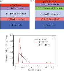
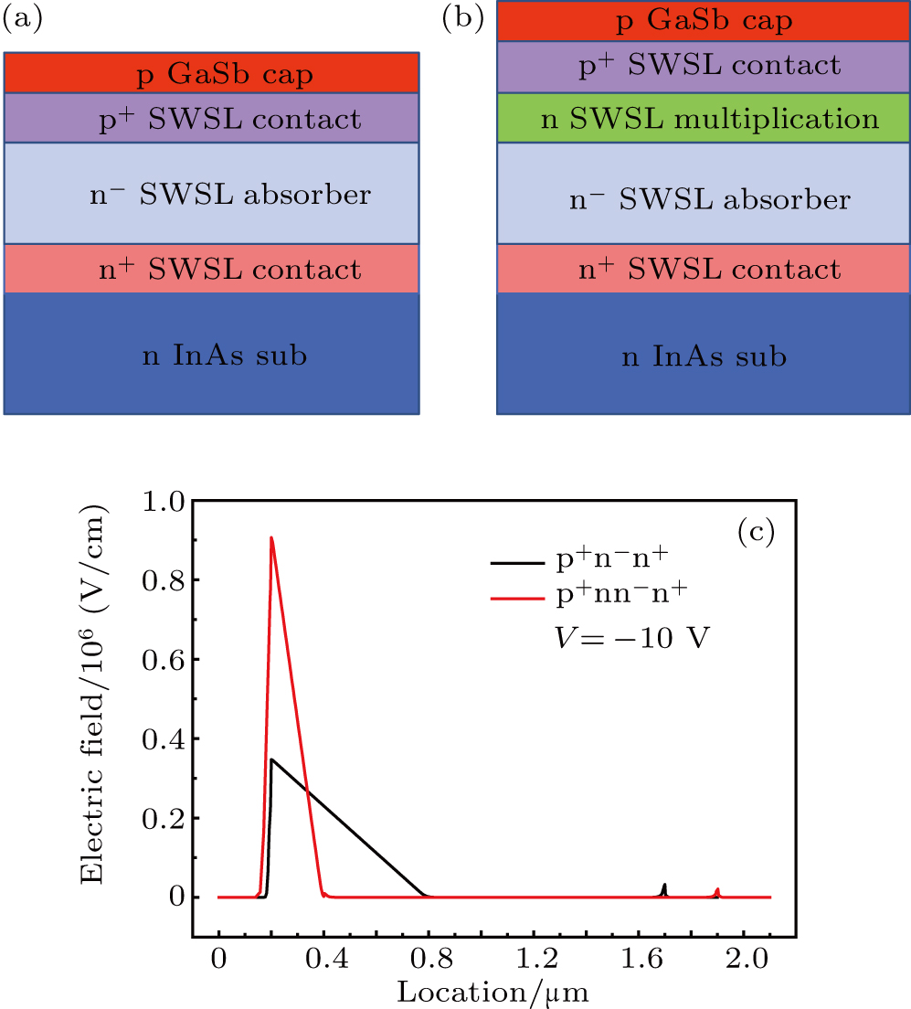
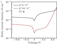
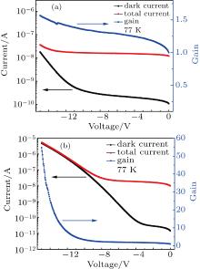
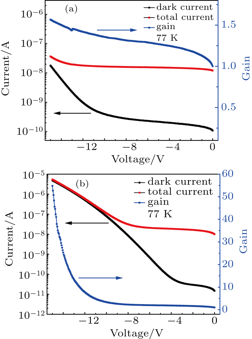
Short-wavelength infrared InAs/GaSb superlattice hole avalanche photodiode

Jia-Feng Liu(刘家丰)1,2, †, Ning-Tao Zhang(张宁涛)4, †, Yan Teng(滕)1,2, Xiu-Jun Hao(郝修军)2,3, Yu Zhao(赵宇)2, Ying Chen(陈影)1,2, He Zhu(朱赫)1,2, Hong Zhu(朱虹)1,2, Qi-Hua Wu(吴启花)2, Xin Li(李欣)2, Bai-Le Chen(陈佰乐)4,§, and Yong Huang(黄勇)1,2,, ‡   

  1. 1 School of Nano-Tech and Nano-Bionics, University of Science and Technology of China, Hefei 230026, China
    2 Key Laboratory of Nanodevices and Applications, Suzhou Institute of Nano-Tech and Nano-Bionics, Chinese Academy of Sciences, Suzhou 215123, China
    3 School of Physical Science and Technology, ShanghaiTech University, Shanghai 201210, China
    4 School of Information Science and Technology, ShanghaiTech University, Shanghai 201210, China
  • Received:2020-05-13 Revised:2020-06-19 Accepted:2020-07-06 Online:2020-11-05 Published:2020-11-03
  • Contact: These authors contributed equally to this work. Corresponding author. E-mail: yhuang2014@sinano.ac.cn §Corresponding author. E-mail: chenbl@shanghaitech.edu.cn
  • Supported by:
    the National Natural Science Foundation of China (Grant Nos. 61874179, 61804161, and 61975121) and the National Key Research and Development Program of China (Grant No. 2019YFB2203400).

Abstract:

We demonstrate two short-wavelength infrared avalanche photodiodes based on InAs/GaSb superlattice grown by metal-organic chemical vapor deposition. The difference between the two devices, namely, p+nn+ and p+nnn+, is that the p+nnn+ device possesses an additional middle-doped layer to separate the multiplication region from the absorption region. By properly controlling the electric field distribution in the p+nnn+ device, an electric field of 906 kV/cm has been achieved, which is 2.6 times higher than that in the p+nn+ device. At a reverse bias of –0.1 V at 77 K, both devices show a 100% cut-off wavelength of 2.25 μm. The p+nn+ and p+nnn+ show a dark current density of 1.5 × 10⁻⁷ A/cm2 and 1.8 × 10⁻⁸ A/cm2, and a peak responsivity about 0.35 A/W and 0.40 A/W at 1.5 μm, respectively. A maximum multiplication gain of 55 is achieved in the p+nnn+ device while the value is only less than 2 in the p+nn+ device. Exponential nature of the gain characteristic as a function of reverse bias confirms a single carrier hole dominated impact ionization.

Key words: short-wavelength infrared, InAs/GaSb superlattice, avalanche photodiodes, metal-organic chemical vapor deposition