Epitaxial growth and air-stability of monolayer Cu2Te
Qian K1, Gao L1, Li H1, Zhang S1, Yan J H1, Liu C2, Wang J O2, Qian T1, 3, Ding H1, 3, Zhang Y Y1, 3, Lin X1, 3, ‡, Du S X1, 3, †, Gao H-J1, 3
Institute of Physics & University of Chinese Academy of Sciences, Chinese Academy of Sciences, Beijing 100190, China
Institute of High Energy Physics, Chinese Academy of Sciences, Beijing 100049, China
CAS Center for Excellence in Topological Quantum Computation, University of Chinese Academy of Sciences, Beijing 100190, China


† Corresponding author. E-mail: sxdu@iphy.ac.cn xlin@ucas.ac.cn

Abstract

A new two-dimensional atomic crystal, monolayer cuprous telluride (Cu2Te) has been fabricated on a graphene-SiC(0001) substrate by molecular beam epitaxy (MBE). The low-energy electron diffraction (LEED) characterization shows that the monolayer Cu2Te forms a superstructure with respect to the graphene substrate. The atomic structure of the monolayer Cu2Te is investigated through a combination of scanning tunneling microscopy (STM) experiments and density functional theory (DFT) calculations. The stoichiometry of the Cu2Te sample is verified by x-ray photoelectron spectroscopy (XPS) measurement. The angle-resolved photoemission spectroscopy (ARPES) data present the electronic band structure of the sample, which is in good agreement with the calculated results. Furthermore, air-exposure experiments reveal the chemical stability of the monolayer Cu2Te. The fabrication of this new 2D material with a particular structure may bring new physical properties for future applications.

1. Introduction

Since the discovery of graphene,[1] the research of two-dimensional (2D) atomic crystal materials has developed rapidly.[24] Transition metal chalcogenides (TMCs) have received much attention because of their diversity and unique properties.[5,6] For example, the non-magnetic silver chalcogenide has been reported for its large magnetoresistance[7] and Ag2Te has been theoretically identified as a new topological insulator.[8] Additionally, TMDCs are well known for their novel optical and electronic properties as well as strong spin–orbit coupling effects.[5,9] TMDCs, such as MoS2, have indirect to direct bandgap arising from their strict dimensional confinement, allowing for applications such as photodetectors and transistors.[1012]

Cu2Te, an important member of the TMCs, has attracted significant attention due to its recent developments in thermoelectric and optoelectronics.[1317] Cu2Te is also commonly used to form back contacts to improve the performance of thin-film solar cell.[1820] However, the structural determination of Cu2Te remains controversial. Although several structures have been proposed experimentally and theoretically,[16,2123] the atomic position in the structure remains unsolved. The hexagonal phase, proposed 70 years ago,[22] has been theoretically proved energetically unfavorable.[23]

In this paper, we report the fabrication of high-quality monolayer Cu2Te on bilayer graphene (BLG)/SiC(0001) by molecular beam epitaxy (MBE) method and the characterization of its structure at atomic level. The stoichiometry and the atomic structure of the monolayer Cu2Te are determined by x-ray photoelectron spectroscopy (XPS), scanning tunneling microscopy (STM), low energy electron diffraction (LEED) experiments and density functional theory (DFT) calculation. We reveal that the monolayer Cu2Te crystallizes in a hexagonal structure with the space group P-3m1. Angle-resolved photoemission spectroscopy (ARPES) is used to study the electronic band structure of the monolayer Cu2Te, and the result is in good agreement with the DFT calculated band structure. Moreover, our experiment shows that the Cu2Te monolayer is quite inert in air. The monolayer Cu2Te with good chemical stability serves as a promising candidate for 2D electronics.

2. Methods

Sample preparation and characterizations The sample was fabricated in a commercial UHV system (Omicron) with standard molecular beam epitaxy (MBE) chamber. The large-scale uniform bilayer graphene on 6H-SiC(0001) wafer was formed by flashing the wafer to 1550 K in ultrahigh vacuum.[24] The quality of the bilayer graphene was verified by LEED and STM. The monolayer Cu2Te sample was fabricated on the bilayer graphene by co-deposition of copper and tellurium atoms from an e-beam evaporator and a standard Knudsen diffusion cell, respectively, while the SiC substrate was held at 400 K during the growth process. The STM, ARPES, LEED, and XPS characterizations were performed at room temperature. ARPES measurements were performed by using the He II ( = 40.6 eV) resonance lines and a VG SCIENTA R4000 analyzer. The angular and energy resolutions were set to 0.2° and 30 meV, respectively. The experiments were carried out with a commercial high-resolution LEED instrument (OCI). Typical emission currents were in the range of 1–5 nA and beam energies were between 0 eV and 120 eV. The XPS experiments were carried out at the Beijing Synchrotron Radiation Facility. The photon energy ranges from 10 eV to 1100 eV. There were four high resolution gratings for realizing the monochromatic synchrotron radiation light.

First-principles calculations Quantum mechanical calculations based on density functional theory (DFT) were performed using the Vienna ab initio simulation package (VASP).[25,26] The projector augmented wave (PAW) method and the local-density approximation (LDA)[27,28] for the exchange–correlation functional were adopted. The rotationally invariant LDA +U formalism proposed by Dudarev et al.[29] was used with Ueff = 6.52 eV for Cu.[30] 450 eV energy cutoff and 15 Å vacuum layers were used for structure relaxations. The total energies were converged to 10-4 eV, and forces were converged to 0.001 eV/Å. The k-points sampling was 39 × 39 × 1.

3. Results and discussion
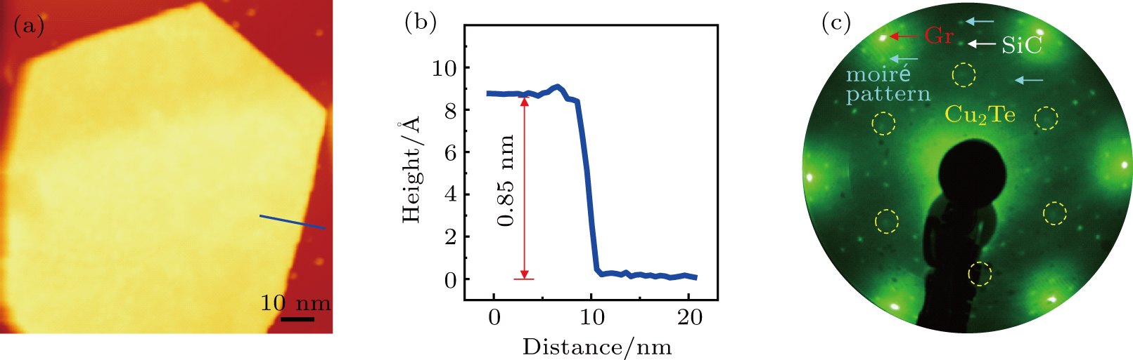
Figure 1(a) shows a typical large scale STM image of the as-grown sample. Cu2Te forms a flat island on bilayer graphene substrate, and the apparent height of the island is ∼ 0.85 nm (Fig. 1(b)), which is measured by the STM line profile crossing the edge of the island (corresponding to the blue line in Fig. 1(a)). The symmetry of Cu2Te on BLG is characterized by LEED. As previously reported,[31] some of the LEED spots originate from the BLG/SiC(0001) substrate. The red, white, and sky-blue arrows point to the spots from BLG, SiC, and moiré pattern, respectively (Fig. 1(c) ). After the growth of Cu2Te, six new diffraction spots appear at the ( ) positions with respect to the graphene spots as indicated by the yellow dashed circles. The LEED pattern of Cu2Te on BLG/SiC(0001) suggests that that the formed Cu2Te island on bilayer graphene is well-ordered.

Fig. 1. Cu2Te island grown on bilayer graphene. (a) An STM topographic image (-1 V, -10 pA) of the Cu2Te island on bilayer graphene. (b) The line profile along the blue line in (a) shows that the apparent height of the Cu2Te island is ∼ 0.85 nm. (c) LEED pattern of Cu2Te grown on bilayer graphene on SiC(0001). The diffraction spots of graphene, SiC, and moiré pattern are indicated by red, white, and sky-blue arrows, respectively. LEED spots indicated by yellow circles originate from Cu2Te, and present a ( ) structure with respect to the graphene substrate.

In order to further investigate the sample in detail, high resolution STM and XPS characterizations were performed. The atomic resolution STM image (Fig. 2(a)) of Cu2Te shows hexagonally arranged protrusions with a lattice constant of ∼ 0.41 nm (Fig. 2(b)). Figures 2(c) and 2(d) are the characteristic XPS spectra from the core levels of Te and Cu, respectively. As shown in Fig. 2(c), the peaks at 583.1 eV and 572.8 eV are assigned to Te 3d3/2 and Te 3d5/2, respectively. In Fig. 2(d), the Cu 2p core level spectrum has two peaks at 952.6 eV (Cu 2p1/2) and 932.8 eV (Cu 2p3/2). All of these XPS results are in good agreement with previous report for nanoflake Cu2Te.[14] It should be emphasized that there is no satellite peaks and all the peaks are sharp, supporting the formation of pure Cu2Te.

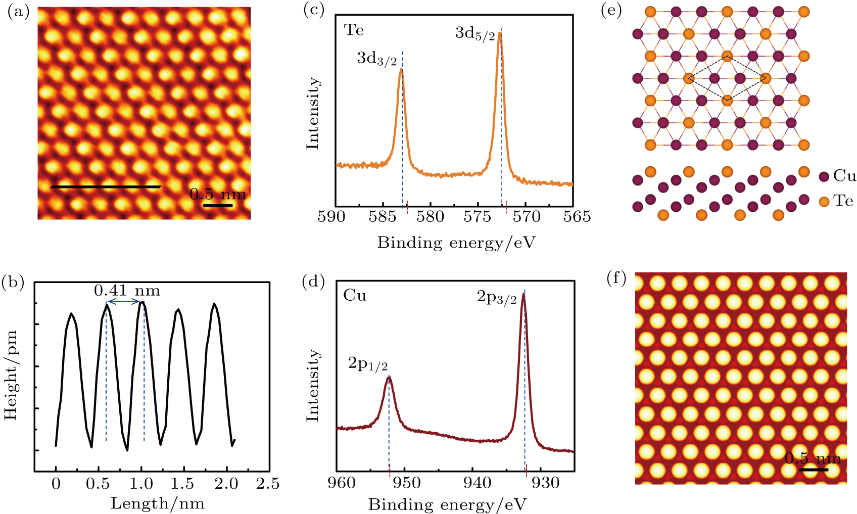
Fig. 2. Atomic configuration and the XPS results of the monolayer Cu2Te. (a) An atomic resolution STM image of monolayer Cu2Te. (b) Line profile of the Cu2Te sample corresponding to the black line in (a). The periodicity of the monolayer Cu2Te lattice is ∼ 0.41 nm. (c) The XPS core-level spectrum of Te. The peak positions are 583.1 eV (3d3/2) and 572.8 eV (3d5/2). (d) The Cu 2p XPS spectrum. The peak positions are 952.6 eV (2p1/2) and 932.8 eV (2p3/2). (e) The atomic model of the monolayer Cu2Te. The dotted rhombus indicates the unit cell of the Cu2Te monolayer. (f) Simulated STM image of the monolayer Cu2Te.

Based on these experimental results and previous prediction of bulk layered Cu2Te,[21] we propose an atomic model of the monolayer Cu2Te, as shown in Fig. 2(e). It contains six atomic layers and the terminated layers are only made of selenium atoms while four copper layers are in the middle. The DFT-calculated relaxed lattice constants are 0.40 nm, which is in agreement with the experimental value of 0.41 nm. Based on this monolayer Cu2Te structure model, we simulate an STM image (Fig. 2(f)), which presents all the features in experimental STM image very well. We unveil the configuration of monolayer Cu2Te at atomic scale for the first time.

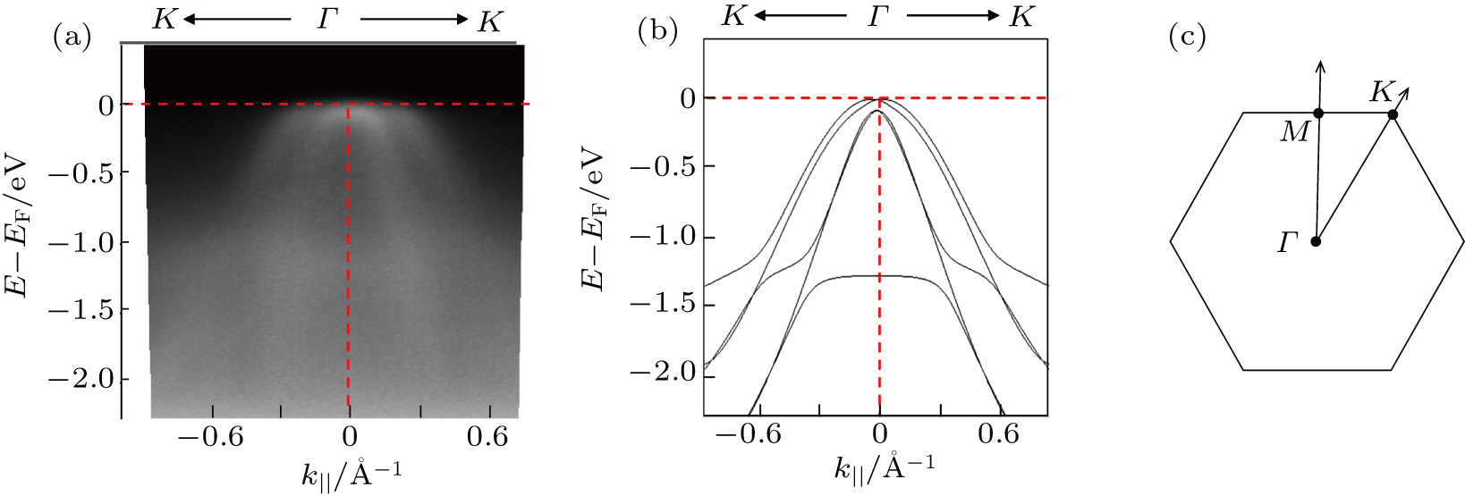
The electronic band structure of the monolayer Cu2Te is investigated by in situ ARPES measurement combing with first-principle calculations. Figure 3(a) is the ARPES result of the monolayer Cu2Te. Along the ΓK direction, the band structure shows a significant feature that there are two degenerate bands around the Fermi surface. To obtain more details of the band structure of the monolayer Cu2Te, the energy bands are calculated based on the monolayer Cu2Te structure model, and presented in Fig. 3(b). It can be seen that the agreement between the ARPES experimental data and the calculated energy bands is quite good. There are four bands around the Fermi level, but they are too close to be distinguished by the ARPES experiment. For the first time, the band structure of the monolayer Cu2Te has been determined experimentally.

Fig. 3. ARPES experimental results and DFT calculated results of the electronic structure of the monolayer Cu2Te. (a) The electronic band structure measured by ARPES along the ΓK direction. (b) The DFT calculated band structure along the ΓK direction. (c) Brillouin zone of the monolayer Cu2Te.

Furthermore, the chemical stability, especially the air stability, is critical for low dimensional materials in practical applications, such as photodetectors and nano-electronic devices. The air-exposure experiment of the monolayer Cu2Te on BLG/SiC(0001) sample was performed. The sample was taken out of the ultra-high vacuum chamber and exposed to air for half an hour. Then, the sample was transferred back into the ultra-high vacuum chamber and mildly annealed at 400 K to remove the possible physisorbed species. Finally, the monolayer Cu2Te was characterized by STM. As shown in Fig. 4(a), the topographic STM image reveals that the Cu2Te island is intact and the island surface is clean and smooth. Figure 4(b) is an atomic resolution STM image of the sample which has been exposed to the air. It is clear that there are no defects and the hexagonal structure remains the same. The air-exposure experiment reveals the chemical robustness of the monolayer Cu2Te, and this chemical inertness makes the monolayer Cu2Te have potential for future applications.

Fig. 4. Air stability of the monolayer Cu2Te. (a) An STM image of a Cu2Te island on bilayer graphene after exposing to air for 30 min (Vs = -1 V, It = 0.1 nA). (b) The high resolution STM image of the Cu2Te surface after exposing to air (Vs = -0.5 V, It = 0.5 nA).
4. Conclusion

We have successfully fabricated monolayer Cu2Te on bilayer graphene/SiC(0001) substrate by the MBE method. The in situ STM, LEED, and XPS measurements verify the quality of the monolayer Cu2Te. An atomic structure model of the monolayer Cu2Te is proposed and DFT calculations confirm the model. Moreover, the ARPES results are in good agreement with the calculated energy bands, which further confirms the structure of the monolayer Cu2Te. Finally, air exposure experiments demonstrate the air stability of the monolayer Cu2Te. Our work provides a new 2D material, Cu2Te, and it has the potential for applications in the future nano-devices.

Reference
[1] Novoselov K S Geim A K Morozov S V Jiang D Zhang Y Dubonos S V Grigorieva I V Firsov A A 2004 Science 306 666
[2] Mounet N Gibertini M Schwaller P Campi D Merkys A Marrazzo A Sohier T Castelli I E Cepellotti A Pizzi G Marzari N 2018 Nat. Nanotech. 13 246
[3] Geim A K Grigorieva I V 2013 Nature 499 419
[4] Hao Y Wang L Liu Y Chen H Wang X Tan C Nie S Suk J W Jiang T Liang T Xiao J Ye W Dean C R Yakobson B I McCarty K F Kim P Hone J Colombo L Ruoff R S 2016 Nat. Nanotech. 11 426
[5] Wang Q H Kalantar-Zadeh K Kis A Coleman J N Strano M S 2012 Nat. Nanotech. 7 699
[6] Yang H Kim S W Chhowalla M Lee Y H 2017 Nat. Phys. 13 931
[7] Xu R A H Rosenbaum T F Saboungi M L Littlewood P B 1997 Nature 390 57
[8] Zhang W Yu R Feng W X Yao Y G Weng H M Dai X Fang Z 2011 Phys. Rev. Lett. 106 156808
[9] Schaibley J R Yu H Clark G Rivera P Ross J S Seyler K L Yao W Xu X 2016 Nat. Rev. Mater. 1 16055
[10] Splendiani A Sun L Zhang Y B Li T S Kim J Chim C Y Galli G Wang F 2010 Nano Lett. 10 1271
[11] Mak K F He K L Shan J Heinz T F 2012 Nat. Nanotech. 7 494
[12] Rivera P Seyler K L Yu H Y Schaibley J R Yan J Q Mandrus D G Yao W Xu X D 2016 Science 351 688
[13] Park D Ju H Oh T Kim J 2018 Sci. Rep. 8 18082
[14] Cheng L Wang M Pei C Liu B Zhao H Zhao H Zhang C Yang H Liu S 2016 RSC. Adv. 6 79612
[15] Ballikaya S Chi H Salvador J R Uher C 2013 J. Mate. Chem. 1 12478
[16] Zhang Y Wang Y Xi L Qiu R Shi X Zhang P Zhang W 2014 J. Chem. Phys. 140 074702
[17] Han C Bai Y Sun Q Zhang S Li Z Wang L Dou S 2016 Adv. Sci. (Weinh) 3 1500350
[18] Yun J H Kim K H Lee D Y Ahn B T 2003 Sol. Energy. Mat. Sol. 75 203
[19] Woodbury H H Aven M 1968 J. Appl. Phys. 39 5485
[20] Lv B Di X Li W Feng L H Lei Z Zhang J Q Wu L L Cai Y P Li B Sun Z 2009 Jpn. J. Appl. Phys. 48 085501
[21] Nguyen M C Choi J H Zhao X Wang C Z Zhang Z Ho K M 2013 Phys. Rev. Lett. 111 165502
[22] Nowotny Z M 1946 Phys. Rep. 37 40
[23] Da Silva J L F Wei S H Zhou J Wu X Z 2007 Appl. Phys. Lett. 91 091902
[24] Wang Q Zhang W Wang L He K Ma X Xue Q 2013 J. Phys: Condens. Matter 25 095002
[25] Kresse G Furthmuller J 1996 Phys. Rev. 54 11169
[26] Kresse G Furthmuller J 1996 Comput. Mater. Sci. 6 15
[27] Ceperley D M Alder B J 1980 Phys. Rev. Lett. 45 566
[28] Perdew J P Zunger A 1981 Phys. Rev. 23 5048
[29] Dudarev S L Botton G A Savrasov S Y Humphreys C J Sutton A P 1998 Phys. Rev. 57 1505
[30] Wu D Zhang Q Tao M 2006 Phys. Rev. 73 235206
[31] Riedl C Coletti C Iwasaki T Zakharov A A Starke U 2009 Phys. Rev. Lett. 103 246804