A facile and efficient dry transfer technique for two-dimensional Van derWaals heterostructure
Xie Li1, 2, Du Luojun1, Lu Xiaobo1, 2, Yang Rong1, 2, †, Shi Dongxia1, 2, Zhang Guangyu1, 2, 3, 4, ‡
Beijing National Laboratory for Condensed Matter Physics and Institute of Physics, Chinese Academy of Sciences (CAS), Beijing 100190, China
School of Physical Science, University of Chinese Academy of Sciences, Beijing 100190, China
Collaborative Innovation Center of Quantum Matter, Beijing 100190, China
Beijing Key Laboratory for Nanomaterials and Nanodevices, Beijing 100190, China


† Corresponding author. E-mail: ryang@iphy.ac.cn gyzhang@iphy.ac.cn

Project supported by the National Basic Research Program of China (Grant Nos. 2013CB934500 and 2013CBA01602), the National Natural Science Foundation of China (Grant Nos. 61325021, 11574361, and 51572289), the Key Research Program of Frontier Sciences, CAS, (Grant No. QYZDB-SSW-SLH004), and the Strategic Priority Research Program (B), CAS (Grant No. XDB07010100).

Abstract

Two-dimensional (2D) Van der Waals heterostructures have aroused extensive concerns in recent years. Their fabrication calls for facile and efficient transfer techniques for achieving well-defined structures. In this work, we report a simple and effective dry transfer method to fabricate 2D heterostructures with a clean interface. Using Propylene Carbonate (PC) films as stamps, we are able to pick up various 2D materials flakes from the substrates and unload them to the receiving substrates at an elevated temperature. Various multilayer heterostructures with ultra-clean interfaces were fabricated by this technique. Furthermore, the 2D materials can be pre-patterned before transfer so as to fabricate desired device structures, demonstrating a facile way to promote the development of 2D heterostructures.

1. Introduction

Heterostructures made of two-dimensional (2D) materials, such as graphene, black phosphorus (BP), and transition metal dichalcogenides (TMDCs), have aroused wide attentions recently due to their unique electrical and optical properties.[15] An essential step for building such 2D heterostructures is via transfer, a challenging process for 2D materials which are atomic-thin and thus vulnerable while being moved.[6] Many research efforts have been devoted to developing proper techniques for stacking different 2D materials to heterostructures in the past few years. However, in the reported approaches, chemical etchants[711] or water[6, 1216] are usually included, which would not only cause the degradation of sample qualities,[12] but also yields contaminated interfaces.[17] As a result, an etching- and water-free transfer method is highly desirable. Although dry transfer methods have been demonstrated by exfoliating 2D materials onto transparent methyl/n-butyl methacrylate copolymer[18] or PDMS,[19] multilayer heterostructures with clean interfaces can hardly be realized. Wang et al. developed a “pick-up” technique by using PDMS/PC/BN to make an assembly of multi-layer heterostructures.[20] The PC films are usually deformed seriously once they have experienced the “pick-up” process, which makes it hard for the following transfer alignment (under the guidance of optical microscope) while fabricating multilayer heterostructures for which multiple “pick-up” processes are required. More importantly, for the above dry transfer methods,[1820] the 2D flakes or early-fabricated 2D heterostructures cannot be pre-patterned before being transferred to construct multilayer heterostructures, which is a critical step for building desired device structures.

Herein, we demonstrate a simple, rapid and efficient dry transfer technique for the fabrication of 2D heterostructures with ultra-clean interfaces. During this transfer process, no chemical etchants and water are applied and the polymer residuals can be easily removed by physically peeling them off and subsequent thermally annealing. Multilayer 2D Van der Waals heterostructures with ideal interfaces can be achieved by multiple transfer steps. Moreover, we are able to pre-pattern the 2D materials before transfer, which is capable of yielding device configurations according to need. Additionally, this method provides a simple and effective way to clean used substrates and improve their reusability.

2. Experimental procedure

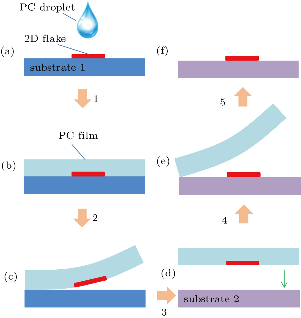
The schematic diagrams of our transfer procedure are illustrated in Fig. 1. The transfer process starts with drop-casting the PC solution on the substrate (S1) with 2D materials on its surface (Fig. 1(a)). The PC solution was prepared by dissolving PC particles into anisole for the mass fraction of ~ 10%. PC curing was performed on the hot plate at 100 °C for 5 minutes (orange arrow 1 in Fig. 1), and the liquid PC can be solidified into a PC film (Fig. 1(b)) acting as a stamp during the following transfer procedure. With very strong adhesion and proper hardness at room temperature (RT), as shown in Fig. 1(c), the PC film is able to carry the 2D flakes out of the substrate surface while being peeled off without obvious deformation (orange arrow 2 in Fig. 1). Subsequently, the PC film carrying 2D flakes can be attached onto any other targeting substrates (S2) (Fig. 1(d)). Owing to the adhesion-weakened behavior of the PC film at elevated temperatures, e.g. 80 °C, the PC film can be easily peeled off with 2D flakes left on the targeting substrate (Fig. 1(e)). PC residuals on the surface of as-transferred 2D materials can be removed by thermally annealing at a temperature of ~ 350 °C in a mixed gas (Ar/H , 150/10 sccm) environment for 3 hours (orange arrow 5 in Fig. 1).

Fig. 1. (color online) (a)–(f) Schematic diagrams of the transfer technique. The transfer process starts with drop-casting the PC solution onto the substrate with 2D flakes on its surface. The following steps are: 1 Baking at 100 °C for 5 min; 2 Peeling off the PC film carrying 2D flakes; 3 Transfer; 4 Heating up to 80 °C and peeling off the PC film; 5 Thermally annealing to remove residuals.
3. Experimental results and discussion

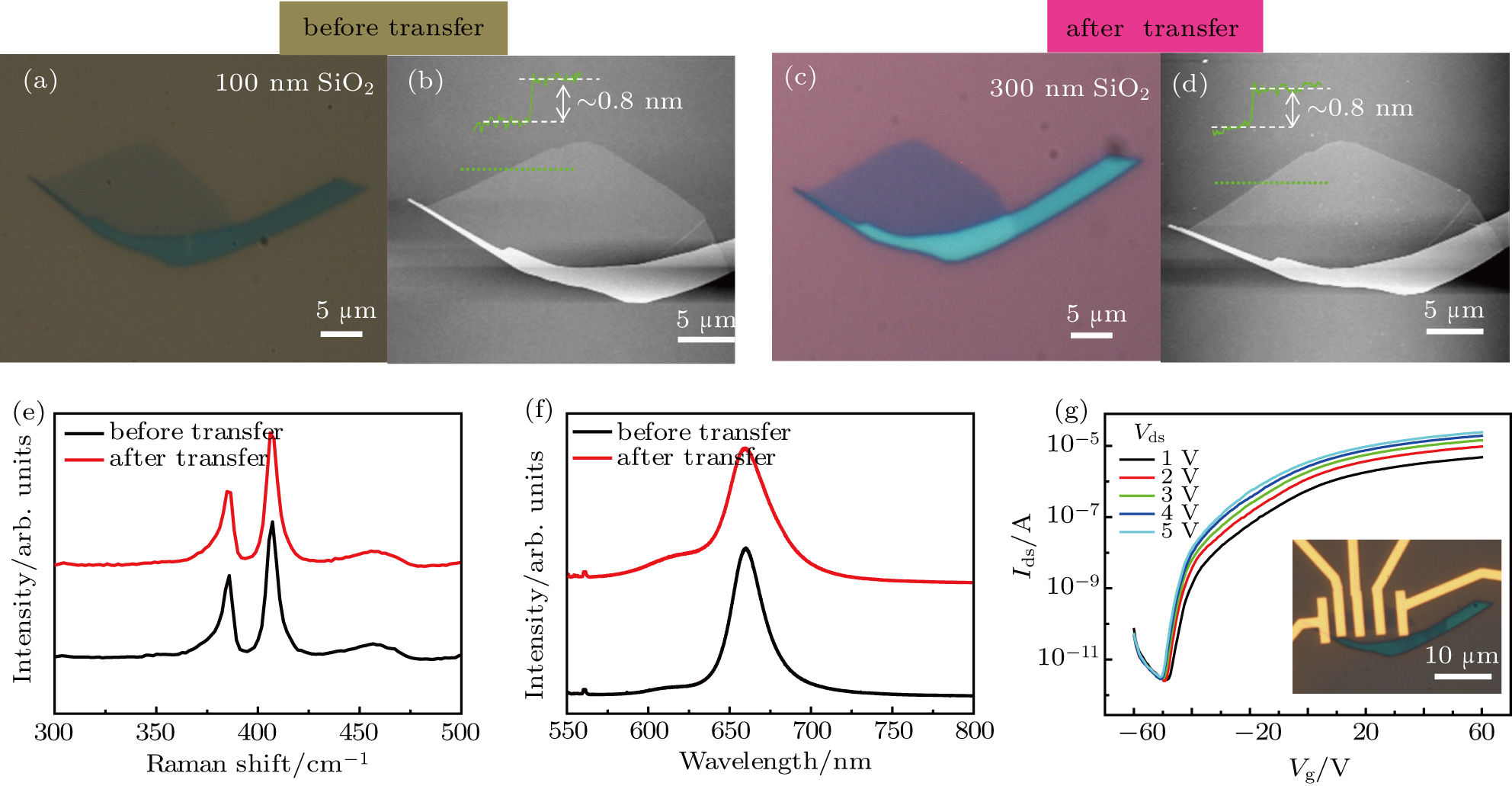
We transferred a mechanically exfoliated monolayer MoS flake from the surface of a 100-nm-SiO /Si substrate to a 300-nm-SiO /Si substrate by the transfer technique described in Fig. 1. Figures 2(a)2(d) are the morphological characterizations of a monolayer MoS flake before and after transfer. Figures 2(a) and 2(c) are the optical microscope (OM) images of the MoS flake before and after the transfer process, respectively. We can see that the MoS flake keeps the same morphology after transfer. We also performed the atomic force microscope (AFM) scanning on the flake surface before (Fig. 2(b)) and after (Fig. 2(d)) transfer. The height profiles from the two AFM images show the thickness (~ 0.8 nm) of the MoS flake and verify its monolayer nature. Comparing the two AFM images, we found that this transfer technique does not introduce winkles or cracks on the sample and the PC residuals after the annealing process are almost negligible which suggests a clean surface of the as-transferred samples. The spectroscopic property comparison is another way to characterize the effects of the transfer. Figure 2(e) shows the Raman spectra, measured under 532-nm excitation light, of the monolayer MoS before and after transfer. No obvious difference was observed while comparing the peak positions or peak spaces between E and A modes. A similar result was found in the photoluminescence (PL) spectra. Both PL spectra show the same band gap ~ 1.88 eV. These characterizations confirm that this transfer technique does not introduce damages into samples. To further evaluate the quality of the transferred samples, we fabricated field-effect transistors (FETs) based on the transferred monolayer MoS sample shown in Fig. 2(c) by EBL and following metal deposition (1-nm Ti and 30-nm Au). A second EBL step and an oxygen plasma etching process were carried out to define the device geometry. The OM image of the as-fabricated FETs is shown in the inset of Fig. 2(g). Typical curves (measured in a close-cycle cryogenic probe station with a base pressure of 10 Torr (1 Torr = 1.333222 Pa) at room temperature) at various bias voltages (Fig. 2(g)) show pronounced n-type characteristics. The ON/OFF ratio and the field-effect mobility are 10 and 27.6 cm s , respectively. These results exhibit no transfer-induced degradation for electrical properties while being compared to the electrical measurements of the FETs based on monolayer MoS without transfer.[2124] Combined morphological, spectroscopic, and electrical characterizations verify that this PC-mediated transfer technique, being free of destructiveness, preserves the initial quality of the 2D materials.

Fig. 2. (color online) Characterizations of a monolayer MoS flake before and after transfer. (a)/(b) OM/AFM image of the monolayer MoS flake before transfer; (c)/(d) OM/AFM image of the monolayer MoS flake after transfer. (e) Raman spectra of the monolayer MoS flake illustrated in panels (a) (black curve) and (c) (red curve); (f) PL spectra of the monolayer MoS flake illustrated in panels (a) (black curve) and (c) (red curve). (f) Transfer characteristics of a monolayer MoS FET based on the flake illustrated in panel (c). Inset: OM image of the device.

This technique is not only able to transfer MoS flakes, but is also suitable for other 2D materials such as graphene, WS , WSe , etc. Figure 3 shows the transfer examples for various 2D materials supported by different substrates. The red arrows stand for the transfer steps. The four transfer examples show that this transfer technique is not material-selective or substrate-selective, i.e., a universal transfer method. In addition, this technique is also suitable to clean used substrates and improve their reusability by drop-casting the PC solution onto the used substrates, heating them for solidification and finally peeling off the solidified PC film. The whole process is simple, fast, and clean.

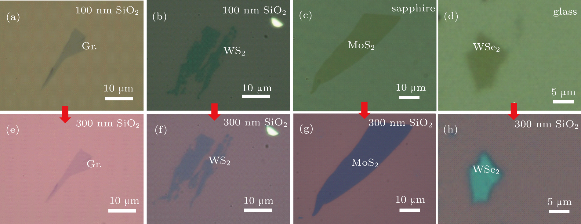
Fig. 3. (color online) Transfer various materials or transfer materials from various substrates. (a)–(d) Graphene, WS , MoS , and WSe flakes on 100-nm SiO , 100-nm SiO , sapphire, and glass substrates, respectively. (e)–(f) Graphene, WS , MoS , and WSe flakes transferred from (a), (b), (c), and (d) onto 300-nm SiO substrates.

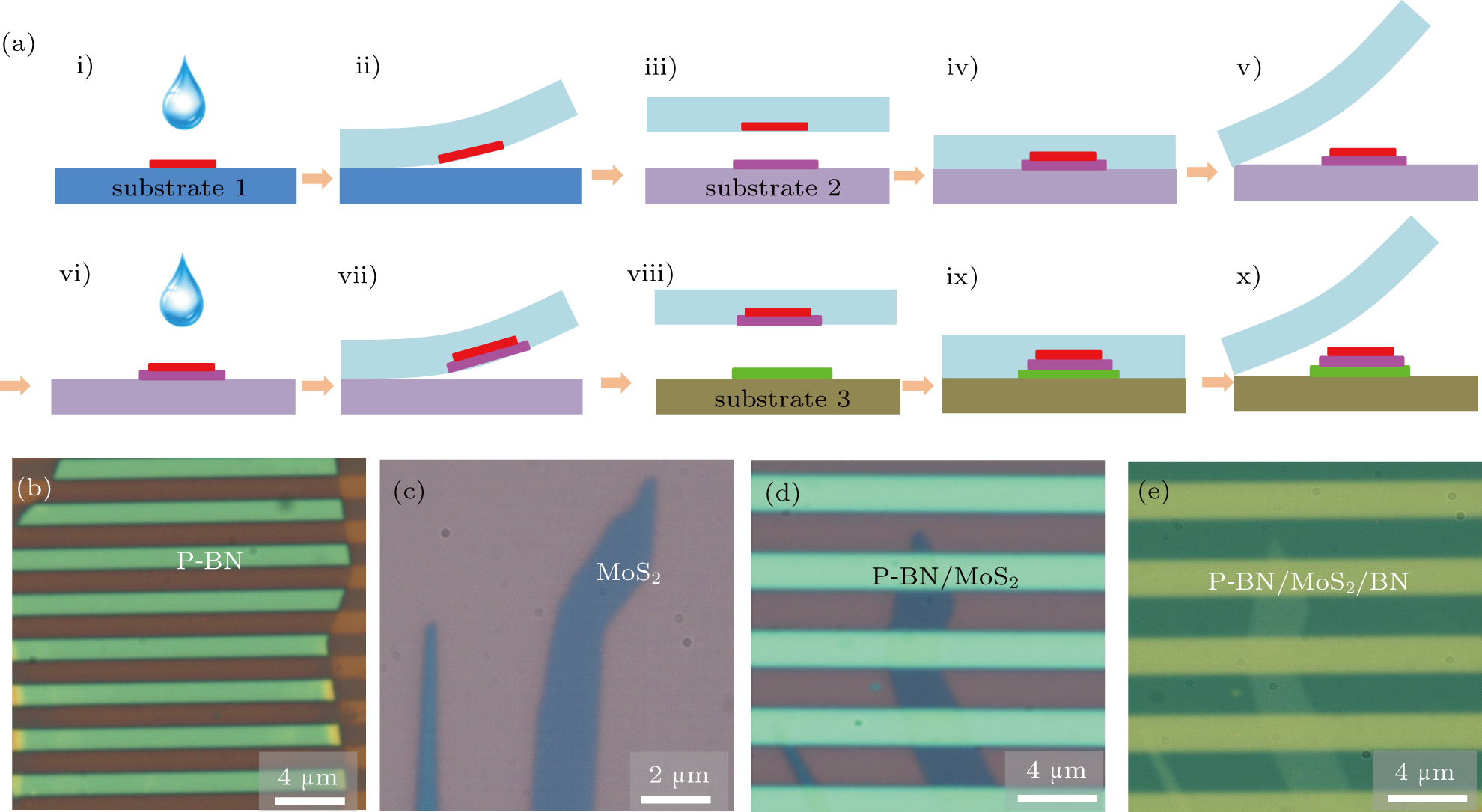
A 2D flake (A) carried by the PC film can also be transferred onto another 2D material (B) to form A/B heterostructure by performing step 3 in Fig. 1 through our home-made point-to-point transfer system. Moreover, the A/B heterostructure could also act as the 2D material in Fig. 1(a) and be further transferred onto any other 2D material (C) to form A/B/C heterostructure by repeating the transfer steps 1 ~ 3 illustrated in Fig. 1. In a similar way, stacked multi-layer 2D heterostructures of A/B/C/D… with clean interface could be realized easily. We later on define this promoted method as the “multilayer-stacking transfer”.

As mentioned above, a 2D flake could be pre-patterned according to need and then transferred (“pre-patterning transfer”). Combining the “multilayer-stacking transfer” and the “pre-patterning transfer” methods, the multilayer heterostructure shown in Fig. 4(e) consists of a MoS flake encapsulated with a pre-patterned boron nitride (BN) flake on top and a normal BN flake underneath. Its fabrication process is schematically displayed in Fig. 4(a): i) PC solution was firstly drop-casted to cover a BN flake which was patterned into an array of stripes with both stripe width and the space distance between the neighboring stripes of 2 μm (Fig. 4(b)). The BN patterning was performed by the EBL process followed by the etching process in the mixed CHCl /O plasma. ii) After the PC solution was solidified into PC film, the pre-patterned BN (p-BN) was picked up by peeling off the PC film. iii) ~ iv) The p-BN was then transferred to cover an exfoliated MoS flake (Fig. 4(c)) supported on a 300-nm SiO /Si substrate. v) Owing to the adhesion-weakening of the PC film at elevated temperature, the PC film was peeled off with p-BN/MoS heterstructure (Fig. 4(d)) left on substrate 2 when heating up to 80 °C. vi) ~ x) The p-BN/MoS can act as the starting material depicted in Fig. 4(a) i) and be transferred onto another BN flake by repeating the process displayed in Fig. 4(a) i) ~ v) to form a p-BN/MoS /BN heterstructure (Fig. 4(e)) in which MoS was partly sandwiched by BN, i.e. the upper surface of the MoS flake was periodically covered by BN stripes while the lower surface fully contacted with the bottom BN. It is noteworthy that the interfaces of the p-BN/MoS /BN heterstructure are clean because the lower surfaces of p-BN and MoS , before being transferred, have only contacted with SiO /Si substrates which are always pre-treated by ultrasonic cleaning in acetone and thermal annealing in oxygen under 500 °C for 2 hours.

Fig. 4. (color online) Construction of a p-BN/MoS /BN heterostructure. (a) Schematic diagrams of the fabrication process of the p-BN/MoS /BN heterostructure. (b) ~ (e) Typical optical images during the transfer process: (b) A BN flake was patterned into a periodic stripe array. (c) An exfoliated MoS flake on a 300-nm SiO substrate. (d) The BN periodic stripe array of panel (b) is transferred to cover the MoS flake of panel (c) to stack p-BN/MoS heterostructure, corresponding to the schematic illustration (a) v). (e) The p-BN/MoS heterostructure of panel (d) is transferred onto a BN flake to stack p-BN/MoS /BN heterostructure by performing the steps illustrated in panel (a) vi) ~ x).

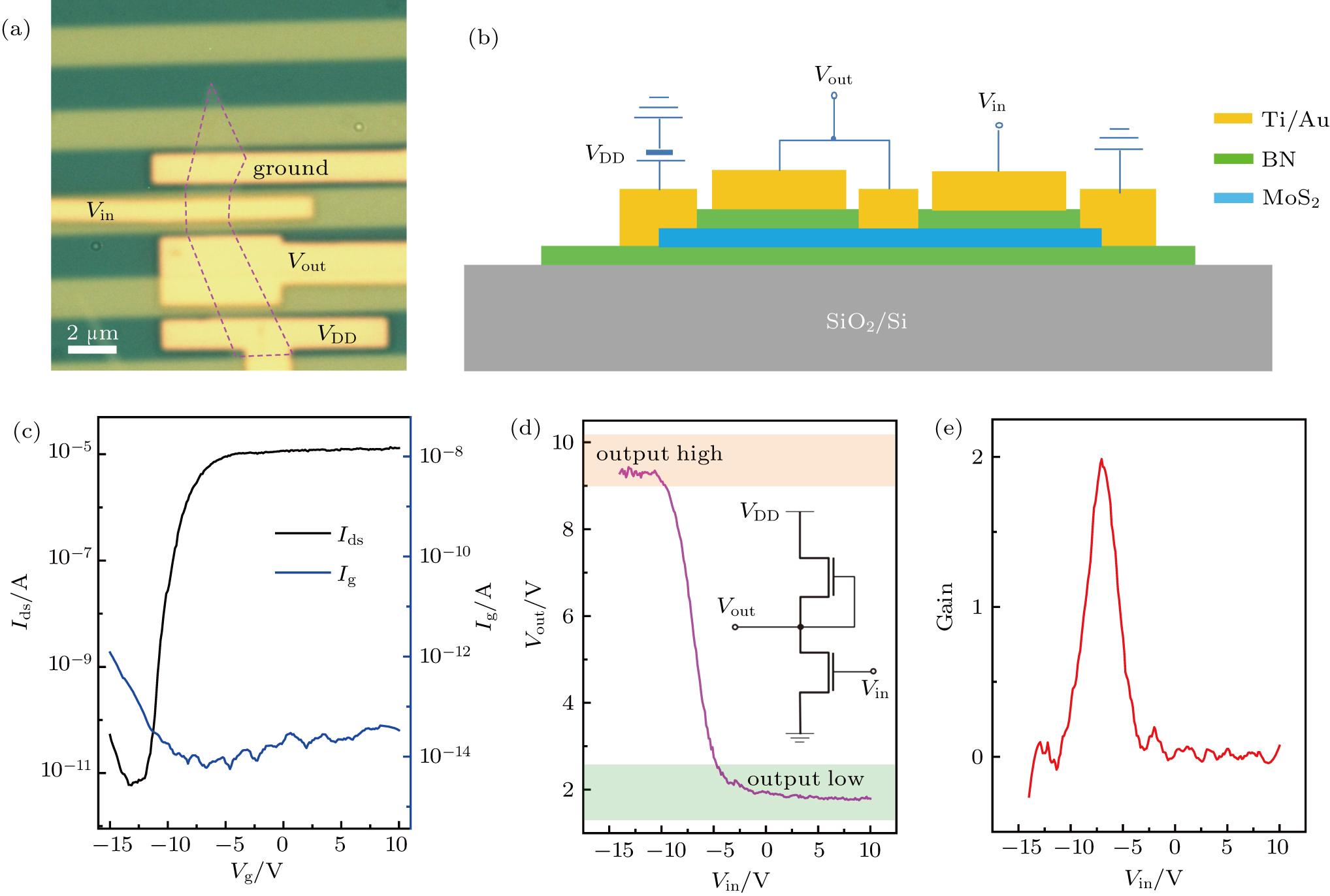
Structures like the p-BN/MoS /BN are very desirable for fabricating logical devices. Because of the p-BN, the upper surface of the MoS flake was periodically divided into bare regions and BN-stripe-covered regions. The bare regions are designed for forming the source–drain contacts by metal-deposition. The BN-stripe-covered regions can act as the conductive channels free of quality degradation or surface scattering due to the encapsulating of BN. What is more, the p-BN stripes act as not only protection layers but also top-gate dielectric layers. With EBL patterning and metal-deposition, the source–drain and top-gate electrodes are formed synchronously. Also note that, in general top-gated device fabricating process,[2527] the source–drain electrodes and top-gate electrodes must be deposited by performing the metal-deposition process twice and the channel region will inevitably contact with polymer resist, which could be entirely avoided by this transfer method.

As shown in Fig. 5(a), we fabricated a logic invertor from the as-fabricated p-BN/MoS /BN structure shown in Fig. 4(e) by EBL and metal (Ti/Au ~ 1 nm/50-nm) deposition. The corresponding schematic diagram of the invertor is shown in Fig. 5(b). There are two top-gated MoS transistors (the “right” and the “left”). The middle electrode and the gate electrode of the “left” transistor are connected together and will operate as an output terminal. In this device configuration, the “right” transistor acts as a switch while the “left” one acts as an effective load. The supply voltage V is applied to the left electrode while the input voltage ( ) is applied to the gate electrode of the “right”. The right electrode is grounded. Thus, the voltage of the output terminal ( ) is the function of . The “right” transistor can operate as an FET whose transfer characteristic under 1-V bias is displayed in Fig. 5(c). Clear n-type behavior with an ON/OFF ratio higher than 10 and a leakage current of pA, very close to the noise level, can be seen, exhibiting good switching properties. Figure 5(d) illustrates the -dependent of the invert from Fig. 5(a). By applying a relative high V (corresponding to logic “1”), the “right” transistor is tuned into ON state and its channel is very conductive that results in a low (logic “0”) close to the grounded value. On the contrary, for low V (corresponding to logic “0”), the “right” transistor is tuned into OFF state and its channel resistance is very high that yields a higher (logic “1”) close to . It is important to examine the changing rate of versus , , which is defined as the invert gain, a significant parameter to evaluate the invert’s capability of amplifying signals. As plotted in Fig. 5(e), at the input range of -9 V V, the invert gain reaches to 2 being similar to some reported MoS invertors.[27, 28] This result also indicates that, in the above mentioned input region, the output voltage changes faster than the input voltage and the invert can realize the function of signal-amplifying.

Fig. 5. (color online) Invertor made from the p-BN/MoS /BN heterostructure. (a) OM image of the invertor based on p-BN/MoS /BN heterostructure in Fig. 4(e) (the fuchsia dotted area indicates the MoS flake). (b) Schematic diagram of the invertor in panel (a). (c) Left axis: typical transfer characteristic curve (@ bias voltage of 1 V) of the MoS channel in the invertor in panel (b). Right axis: corresponding leakage currents in the transfer characteristic measurement. (d) Output voltages as a function of input voltages. Inset is the schematic drawing of the electronic circuit. (e) -dependence of the invert gain.
4. Conclusion

We have developed a simple, facile, and universal approach to transfer 2D flakes in a fast, efficient, and nondestructive manner. PC films act as the stamps during the transfer process. This dry transfer step and nearly residual-free process can reliably yield multi-layer 2D heterostructures with clean interfaces. This technique also allows a pre-patterning of the 2D materials before the transfer for construction of complex stacking structures according to need.

Reference
[1] Yu W J Li Z Zhou H L Chen Y Wang Y Huang Y Duan X F 2013 Nat. Mater. 12 246
[2] Gong Y J Lin J H Wang X L Shi G Lei S D Lin Z Zou X L Ye G L Vajtai R Yakobson B I Terrones H Tay B K Lou J Pantelides S T Liu Z Zhou W Ajayan P M 2014 Nat. Mater. 13 1135
[3] Liu Y Weiss N O Duan X D Cheng H C Huang Y Duan X F 2016 Nat. Rev. Mater. 1 16042
[4] Chiu M H Zhang C D Shiu H W Chuu C P Chen C Y Chang C Y S Chen C H Chou M Y Shih C K Li L J 2015 Nat. Commun. 6 7666
[5] Kośmider K Fernández-Rossier J 2013 Phys. Rev. 87
[6] Li X S Zhu Y W Cai W W Borysiak M Han B Y Chen D Piner R D Colomb L Ruff R S 2009 Nano Lett. 9 4359
[7] Gao L B Ni G X Liu Y P Liu B Neto A H C Loh K P 2014 Nature 505 190
[8] Elias A L Perea-Lpez N Castro-Beltrán A Berkdemir A Lv R Feng S M Long A D Hayashi T Kim Y A Endo M Gutiérrez H R Pradhan N R Balicas L Mallourk T L Lpez-Urías F Terrones H Terrones M 2014 ACS Nano 7 5235
[9] Chen X D Li Z B Zheng C Y Xing F Yan X Q Chen Y S Tian J G 2013 Carbon 56 271
[10] Reina A Son H Jiao L Y Fan B Dresselhaus M S Liu Z F Kong J 2008 J. Phys. Chem. Lett. 112 17741
[11] Her M Beams R Novotny L 2013 Phys. Lett. 377 1455
[12] Lee C H McCulloch W Lee E W II Ma L Krishnamoorthy S Hwang J Wu Y Y Rajan S 2015 Appl. Phys. Lett. 107 193503
[13] Schneider G F Calado V E Zandbergen H Vandersypen L M Dekker C 2010 Nano Lett. 10 1912
[14] Gurarslan A Yu Y F Su L Q Yu Y L Suarez F Yao S S Zhu Y Ozturk M Zhang Y Cao L Y 2014 ACS Nano 8 11522
[15] Li H Wu J Huang X Yin Z Liu J Zhang H 2014 ACS Nano 8 6563
[16] Ma D L Shi J P Ji Q Q Chen K Yin J B Lin Y W Zhang Y Liu M X Feng Q L Song X J Guo X F Zhang J Zhang Y F Liu Z F 2015 Nano Res. 8 3662
[17] Zhang J Wang J H Chen P Sun Y Wu S Jia Z Y Lu X B Yu H H Chen W Zhu J Q Xie G B Yang R Shi D X Xu X L Xiang J Y Liu K H Zhang G Y 2016 Adv. Mater. 28 1950
[18] Zoomer P J Dash S P Tombros N Wees B J 2011 Appl. Phys. Lett. 99 232104
[19] Castellanos-Gomez A Buscema M Molenaar R Singh V Janssen L Herre S J van der Zant Steele G A 2014 2D Materials 1 011002
[20] Wang L Meric I Huang P Gao Q Gao Y Tran H Taniguchi T Watanabe K Campos L Muller D 2013 Science 342 614
[21] Kwak J Y Hwang J Calderon B Alsalman H Munoz N Schutter B Spencer M G 2014 Nano Lett. 14 4511
[22] Yu H Yang Z Z Du L J Zhang J Shi J N Chen W Chen P Liao M Z Zhao J Meng J L Wang G L Zhu J Q Yang R Shi D X Zhang G Y 2017 Small 13
[23] Zhao J Yu H Chen W Yang R Zhu J Q Liao M Z Shi D X Zhang G Y 2016 ACS Appl. Mater. Interfaces 8 16546
[24] Zhang J Yu H Chen W Tian X Z Liu D H Cheng M Xie G B Yang W Yang R Bai X D Shi D X Zhang G Y 2014 ACS Nano 8 6024
[25] Radisavljevic B Radenovic A Brivio J Giacometti V Kis A 2011 Nat. Nanotechnol. 6 147
[26] Lee H S Min S W Park M K Lee Y T Jeon J Kim J H Ryu S Lm S 2012 Small 8 3111
[27] Radisavljevic B Whitwick M B Kis A 2011 ACS Nano 5 9934
[28] Xu K Chen D X Yang F Y Wang Z X Yin L Wang F Cheng R Q Liu K H Xiong J Liu Q He J 2017 Nano Lett. 17 1065