A facile and efficient dry transfer technique for two-dimensional Van derWaals heterostructure
Xie Li1, 2, Du Luojun1, Lu Xiaobo1, 2, Yang Rong1, 2, †, Shi Dongxia1, 2, Zhang Guangyu1, 2, 3, 4, ‡
       

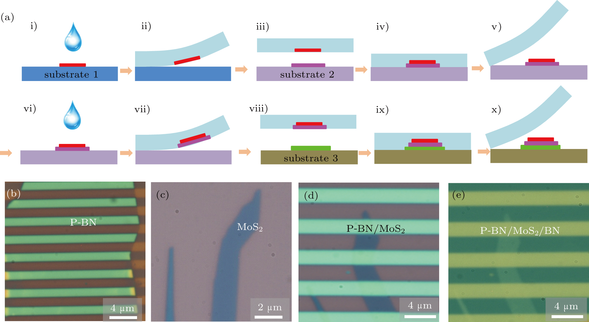
(color online) Construction of a p-BN/MoS /BN heterostructure. (a) Schematic diagrams of the fabrication process of the p-BN/MoS /BN heterostructure. (b) ~ (e) Typical optical images during the transfer process: (b) A BN flake was patterned into a periodic stripe array. (c) An exfoliated MoS flake on a 300-nm SiO substrate. (d) The BN periodic stripe array of panel (b) is transferred to cover the MoS flake of panel (c) to stack p-BN/MoS heterostructure, corresponding to the schematic illustration (a) v). (e) The p-BN/MoS heterostructure of panel (d) is transferred onto a BN flake to stack p-BN/MoS /BN heterostructure by performing the steps illustrated in panel (a) vi) ~ x).