Liang Feng, Chen Ping, Zhao De-Gang, Jiang De-Sheng, Zhao Zhi-Juan, Liu Zong-Shun, Zhu Jian-Jun, Yang Jing, Liu Wei, He Xiao-Guang, Li Xiao-Jing, Li Xiang, Liu Shuang-Tao, Yang Hui, Zhang Li-Qun, Liu Jian-Ping, Zhang Yuan-Tao, Du Guo-Tong. Observation of positive and small electron affinity of Si-doped AlN films grown by metalorganic chemical vapor deposition on n-type 6H–SiC. Chinese Physics B, 2016, 25(5): 057703
Permissions
Observation of positive and small electron affinity of Si-doped AlN films grown by metalorganic chemical vapor deposition on n-type 6H–SiC
Liang Feng1, Chen Ping1, †, , Zhao De-Gang1, Jiang De-Sheng1, Zhao Zhi-Juan2, Liu Zong-Shun1, Zhu Jian-Jun1, Yang Jing1, Liu Wei1, He Xiao-Guang1, Li Xiao-Jing1, Li Xiang1, Liu Shuang-Tao1, Yang Hui3, Zhang Li-Qun3, Liu Jian-Ping3, Zhang Yuan-Tao4, Du Guo-Tong4
State Key Laboratory on Integrated Optoelectronics, Institute of Semiconductors, Chinese Academy of Sciences, Beijing 100083, China
Center for Physicochemical Analysis and Measurement, Institute of Chemistry, Chinese Academy of Sciences, Beijing 100190, China
Suzhou Institute of Nano-tech and Nano-bionics, Chinese Academy of Sciences, Suzhou 215123, China
State Key Laboratory on Integrated Optoelectronics, College of Electronic Science and Engineering, Jilin University, Changchun 130023, China
† Corresponding author. E-mail: pchen@semi.ac.cn
Project supported by the National Natural Science Foundation of China (Grant Nos. 61574135, 61574134, 61474142, 61474110, 61377020, 61376089, 61223005, and 61321063), the One Hundred Person Project of the Chinese Academy of Sciences, and the Basic Research Project of Jiangsu Province, China (Grant No. BK20130362).
Abstract
Abstract
We have investigated the electron affinity of Si-doped AlN films (NSi = 1.0 × 10¹⁸–1.0 × 1019 cm−3) with thicknesses of 50, 200, and 400 nm, synthesized by metalorganic chemical vapor deposition (MOCVD) under low pressure on the n-type (001)6H–SiC substrates. The positive and small electron affinity of AlN films was observed through the ultraviolet photoelectron spectroscopy (UPS) analysis, where an increase in electron affinity appears with the thickness of AlN films increasing, i.e., 0.36 eV for the 50-nm-thick one, 0.58 eV for the 200-nm-thick one, and 0.97 eV for the 400-nm-thick one. Accompanying the x-ray photoelectron spectroscopy (XPS) analysis on the surface contaminations, it suggests that the difference of electron affinity between our three samples may result from the discrepancy of surface impurity contaminations.
Aluminum nitride, as a representative of wideband gap semiconductors with a large bandgap of about 6.2 eV, has attracted extensive attention due to its excellent physical and stable chemical properties.[1] AlN plays an important role in achieving wonderful performance on ultraviolet (UV) devices, such as light-emitting diodes,[2] detectors,[3] and lasers.[4] Especially, since Benjamin[5] predicted a negative electron affinity (NEA) of AlN on 6H–SiC substrate, even there were some disputations on the value of its electron affinity,[6] the interest in field-emission (FE) applications of AlN materials has grown because the material with NEA can be applied in vacuum microelectronic devices as a cold cathode, where the vacuum level is pulled below the conduction band minimum and electrons can be freely extracted from the surface of material to the vacuum environment. Thus, the vacuum microelectronic devices can obtain a low value of threshold voltage and a large value of electron field emission (FE) current. Significant progress has been made to apply AlN on vacuum microelectronic devices, such as field emission displays and micro-vacuum-tubes.[7–9] However, electron affinity of a semiconductor sample may be affected by the surface dipole and the defect energy levels on the surface of the material,[10] thus it is also related to the sample preparation condition and to the chemical composition of the surface area.[6] In the present study, we investigated the electron affinity of AlN film grown by metalorganic chemical vapor deposition (MOCVD) on n-typed SiC substrate in detail through photoelectron spectroscopy, and found a positive and low electron affinity of the MOCVD grown AlN films, which is related to the discrepancy of surface impurity contaminations.
2. Experimental setup
The samples used in this work were Si-doped AlN films with thicknesses of 50, 200, and 400 nm, which were grown directly on the n-type (001) 6H–SiC substrates at 1100 °C by metalorganic chemical vapor deposition (MOCVD) under a low pressure. A heterogeneous SiC substrate is preferred to be employed due to their close lattice constants of about 3.1 Å and relatively high thermal expansion coefficient of about 4.2× 10⁻⁶ K−1 along the a axis, which would benefit the crystal quality of epitaxial AlN layers.[11] The precursors of Al and N were trimethylaluminum (TMA) and ammonia (NH3), with flow rates of 60 sccm (standard-state cubic centimeter per minute) and 500 sccm, respectively. The precursor of Si-dopant was silane (SiH4) and its flow rate was 1 sccm. Thus, by controlling the synthesizing time, three Si-doped AlN layers were grown with different thicknesses, i.e., 50 nm, 200 nm, and 400 nm. The concentration of Si-dopant in the AlN layer was estimated to be in the order of 1.0× 10¹⁸–1.0× 1019 cm−3 according to the secondary ion mass spectroscopy measurement.
Before carrying out UPS measurements, the samples were cut into about 1 cm×1 cm tablets and then surface treated carefully with acetone, alcohol, deionized water, and dilute hydrochloric acid. Then, the photoelectron spectroscopy measurements were performed using ESCALab 250Xi photoelectron spectroscopy. During the UPS analysis, the tablet of AlN film was mounted on a stainless steel sample holder with a copper clip, and the helium pressure in the analysis chamber was about 2× 10⁻⁸ mbar. The He I (21.2 eV) emission line was employed as the UPS excitation source and the intensity of photo-excited electrons is recorded as a function of electron kinetic energy in the UPS spectrum. Furthermore, the ionization energy (I) of the AlN sample can be directly determined through the UPS spectrum as the following expression:[5,10,12,13]
where hν and W are the photon energy (He I, 21.2 eV) and the width of UPS spectrum, respectively, and thus the electron affinity (χ) could be[5,10,12,13]
where Eg is the band gap of the semiconductor. Here, the width W is derived from the onset of the low kinetic energy limit to the end of the high kinetic energy limit in the UPS spectrum, corresponding to the inelastic secondary electron cutoff (SECO) and the valence band maximum (VBM), respectively.
After the UPS measurement, the elements on the AlN surface were analyzed by x-ray photoelectron spectroscopy where the x-ray source is from a monochromatic Al Kα radiation of 1486.6 eV operated at 250 W, whose energy resolution was around 0.6 eV. The base pressure in the analysis chamber was about 2×10⁻⁹ mbar (1 bar = 105 Pa). While taking the XPS measurement, the electron beam was focused on a round-hole region about 500-μm diameter.
3. Results and discussion
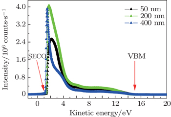
The results of UPS measurements conducted on the AlN film samples with thicknesses of 50 nm, 200 nm, and 400 nm, are shown in Fig. 1, which were obtained with a −10 V bias to shift the spectrum away from the spectrometer’s work function effect and make the spectrum structure clearer. As mentioned before, the inelastic secondary electron cutoff (SECO) and the valence band maximum (VBM) are assigned to the emission onset edge at the low and high kinetic energy limits, respectively, which are schematically marked by arrows in Fig. 1. It is noted that the position of the inelastic secondary electron cutoff shows a tiny shift to low kinetic energy with increasing thickness of AlN films, which may be related to the difference in charging effect for these three samples although the AlN layers were deposited on Si-doped SiC substrates to reduce the influence of the poor conductive character of the wide-band-gap AlN on UPS measurement. However, the charging effect does not affect the width of energy distribution of UPS analysis, because we have applied enough high bias to discern the entire width of the spectra during UPS measurements. Furthermore, all three UPS spectra present an intense and narrow emission peak at the low kinetic energy end of photoemission spectra. van der Weide and his co-workers[14,15] also found this intense and narrow emission peak when they studied the electron affinity of the (100)C surface, and they assigned it to the negative electron affinity (NEA). However, Wu and Kahn[6] reasonably demonstrated that this peak was due to huge secondary electrons thermalized to conduction-band minimum at the surface instead of NEA, and these thermalized electrons were free to escape from the solid, contributing the photoemission peak at the low kinetic energy end of the measured UPS spectra.
Fig. 1. The UV photoemission spectra of AlN films grown on n-type 6H–SiC. The inelastic secondary electron cutoff and the valence band maximum are marked as SECO and VBM, respectively.
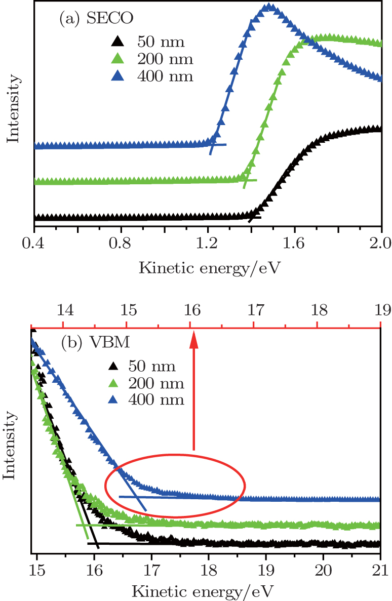
In order to obtain the value of electron affinity, the width of the UPS spectra shown in Fig. 1 is verified first. Here, a linear extrapolation is used to exactly determine the inelastic secondary electron cutoff and the valence band maximum by the intersection of the intensity curve tangent and the base line. In Fig. 2(a), the inelastic secondary electron cutoff (SECO) of these three samples is obtained from a linear extrapolation of the emission onset edge to zero intensity at the low kinetic energy limit. The SECO is obtained as 1.41 eV for 50-nm-thick AlN film, 1.38 eV for the 200-nm-thick one and 1.23 eV for the 400-nm-thick one. In addition, in Fig. 2(b), the VBM of these three samples is determined by the intersection point of the tangent of the UPS intensity curve with the base line at the high kinetic energy limit, i.e., 16.05 eV for 50-nm-thick AlN film, 15.8 eV for the 200-nm-thick one, and 15.26 eV for the 400-nm-thick one. Thus, the widths W of UPS spectra of these three AlN samples are determined to be 14.91 eV, 14.42 eV, and 14.03 eV, respectively. Combined with the data of the band gap (Eg) of AlN as 6.2 eV and the photon energy (hν) of 21.2 eV, the electron affinity (χ) is obtained through Eq. (2), i.e., 0.36 eV for 50-nm-thick AlN film, 0.58 eV for the 200-nm-thick one, and 0.97 eV for the 400-nm-thick one. The entire results are presented in Table 1.
As displayed in Figs. 1 and 2, and Table 1, the overall UPS analysis demonstrates that the electron affinity for our three AlN simples is positive and small rather than negative, i.e., 0.36 eV for 50-nm-thick AlN film, 0.58 eV for the 200-nm-thick one, and 0.97 eV for the 400-nm-thick one. It indicates that thinner AlN film may possess a better performance of field emission due to its smaller electron affinity value.
Fig. 2. The SECO (a) and VBM (b) of AlN film samples with thicknesses of 50 nm, 200 nm, and 400 nm. The lines and triangular symbols present the fitting curves and UPS data, respectively.
Table 1.
Table 1.
Table 1.
The electron affinity for AlN film samples through UPS measurement.
.
Film thickness/nm
SECO/eV
VBM/eV
χ/ eV
50
1.41
16.05
0.36
200
1.38
15.8
0.58
400
1.23
15.26
0.97
Table 1.
The electron affinity for AlN film samples through UPS measurement.
.
It is noted that Benjamin[5] reported a negative electron affinity for the AlN film grown by molecular beam epitaxy (MBE). However, Wu et al. later on demonstrated a positive electron affinity of 2.1 eV[6] or 1.9 eV[16] for a 0.2-mm-thick AlN layer grown by MBE, where the values of electron affinity are much larger than our values. We think the difference in the measured electron affinity values between our three samples of different thicknesses, and between our results and those reported in Refs. [6] and [16] might be caused by the difference of surface contaminations, especially oxygen contamination, because the measured electron affinity depends on many factors, including the presence of adsorbates and surface dipoles.
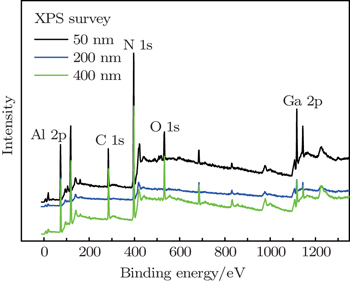
As shown in Fig. 3, the results of the x-ray photoelectron spectroscopy survey scans indicate that the surfaces of these three AlN film samples are composed of the Ga, C, and O contaminants, besides the Al and N elements, which are marked as the peaks of Ga 2p, C 1s, O 1s, Al 2p, and N 1s, respectively. For the O and C elements, during the MOCVD growth, due to the precursors of Al and N, i.e., trimethylaluminum and ammonia, respectively, hydrocarbon and oxygen can be induced into AlN films. On the other hand, for the Ga element, it is suspected that it comes from a residual impurity after GaN or GaAs film growth due to the incompletely clean vacuum chamber of our MOCVD system. However, the XPS survey could not reveal the Si dopant due to a strong interference between the Si 2p peak and the energy loss peak of the Al element. In addition, the elements with a small atomic number, such as the H element, cannot be detected by XPS because of its small photo-ionization cross-section. As shown in Table 2, the contents of these five elements of the 50-nm, 200-nm, and 400-nm-thick AlN films are expressed by the values of atom percentage (at.%).
Fig. 3. XPS spectra of AlN film samples with thicknesses of 50 nm, 200 nm, and 400 nm.
Table 2.
Table 2.
Table 2.
XPS quantification of elemental composition on AlN film surface.
.
Thickness/nm
Atomic percentage /at.%
Ga
Al
O
C
N
50
2.04
41.76
4.93
17.68
33.59
200
1.17
41.14
5.43
13.91
38.35
400
0.93
39.56
8.39
22.54
28.58
Table 2.
XPS quantification of elemental composition on AlN film surface.
.
It was reported that the surface O would result in a change in the surface dipole and influence on the electron affinity.[10] It was also found that oxygen absorption or residual oxygen impurities distributed in the bulk AlN and AlGaN could increase the ionization energy of AlN and AlGaN, and thus their electron affinity.[6,17,18] For our three AlN samples, the content of the oxygen element presents an increase with thickness increasing, i.e., 4.93%, 5.43%, and 8.39% for the 50-nm, 200-nm, and 400-nm-thick AlN samples, respectively, which suggests that the different electron affinity of our three AlN film samples with different thicknesses may be resulted from the different contents of surface O element. It is suspected that more O atoms would be introduced while there is a longer growth time for growing a thicker layer and change the surface of AlN films, thus affect the electron affinity.
It is also noted that Kasu and Kobayashi[18] also reported a thickness dependence, but different from ours. They claimed that the 400-nm-thick Si-doped AlN film has a better character of field emission compared with 100-nm, 200-nm, and 800-nm-thick AlN films, where the concentration of Si dopant is in an order of 1 × 1021 cm−3.[19,20] In our previous research, Shi et al.,[21] reported that the Si-doped AlN has a rougher surface than the un-doped one. Therefore, the different results between ours and Refs. [19] and [20] may be that, the heavy Si-doping may induce a more significant ridge structure on the surface of the AlN epitaxial layer, where the surface morphology has a larger influence on the distribution of local electric field on the surface and results in a larger field enhancement factor, thus a better performance of field emission. However, the difference of the electron affinity is not enough to be reflected. Actually, the electron affinity of their samples may also present a small increase with increasing thickness.
4. Conclusion
We have synthesized Si-doped AlN films (NSi = 1.0× 10¹⁸–1.0× 1019 cm−3) with thicknesses of 50 nm, 200 nm, and 400 nm, by low pressure metalorganic chemical vapor deposition on the n-type (001) 6H–SiC substrates. Positive and small values of electron affinity of these three AlN samples are observed through the ultraviolet photoelectron spectroscopy in an ultrahigh vacuum system, i.e., 0.36 eV for 50-nm-thick AlN film, 0.58 eV for the 200-nm-thick one, and 0.97 eV for the 400-nm-thick one. In addition, the x-ray photoelectron spectroscopy result indicates that an increase of the electron affinity with increasing thickness may be related to the different surface contamination.
Observation of positive and small electron affinity of Si-doped AlN films grown by metalorganic chemical vapor deposition on n-type 6H–SiC
[Liang Feng1, Chen Ping1, †, , Zhao De-Gang1, Jiang De-Sheng1, Zhao Zhi-Juan2, Liu Zong-Shun1, Zhu Jian-Jun1, Yang Jing1, Liu Wei1, He Xiao-Guang1, Li Xiao-Jing1, Li Xiang1, Liu Shuang-Tao1, Yang Hui3, Zhang Li-Qun3, Liu Jian-Ping3, Zhang Yuan-Tao4, Du Guo-Tong4]


 , Zhao De-Gang1, Jiang De-Sheng1, Zhao Zhi-Juan2, Liu Zong-Shun1, Zhu Jian-Jun1, Yang Jing1, Liu Wei1, He Xiao-Guang1, Li Xiao-Jing1, Li Xiang1, Liu Shuang-Tao1, Yang Hui3, Zhang Li-Qun3, Liu Jian-Ping3, Zhang Yuan-Tao4, Du Guo-Tong4]