Project supported by the National Basic Research Program of China (Grant No. 2011CBA00602) and the National Science and Technology Major Project of the Ministry of Science and Technology of China (Grant No. 2011ZX02708-002).
Abstract
Abstract
Various biaxial compressive strained GaSb p-channel metal–oxide–semiconductor field-effect transistors (MOSFETs) are experimentally and theoretically investigated. The biaxial compressive strained GaSb MOSFETs show a high peak mobility of 638 cm2/V·s, which is 3.86 times of the extracted mobility of the fabricated GaSb MOSFETs without strain. Meanwhile, first principles calculations show that the hole effective mass of GaSb depends on the biaxial compressive strain. The biaxial compressive strain brings a remarkable enhancement of the hole mobility caused by a significant reduction in the hole effective mass due to the modulation of the valence bands.
High mobility III–V semiconductors have attracted a great deal of attention, they are considered as candidates to replace strained-Si in future high-performance metal–oxide–semiconductor field-effect transistors (MOSFETs).[1–3] Recent studies on III–V MOSFETs focus on gate-stack and interface engineering.[4,5] Many high performance III–V channel MOSFETs have been reported.[6–9] However, research on p-channel III–V MOSFETs has traditionally lagged in comparison to n-channel III–V MOSFETs.[10] GaSb has very high hole mobility (∼1000 cm2/V·s), making it attractive as an alternative channel material to silicon, especially for the p-channel MOSFET application.[10–12] The hole mobility of GaSb is twice as high as that of silicon and GaAs.[13] To date, many efforts have been made for the GaSb MOSFET application, such as the source/drain technology and the gate stacks technology.[14,15] Although GaSb MOSFETs have been demonstrated by some research groups, further improvements in the performance of GaSb p-channel MOSFETs are badly needed. If the hole mobility of GaSb can be further enhanced, GaSb p-channel MOSFETs will obtain a wide range of applications in the future.
Strain engineering is considered as one of the most promising technologies to improve the mobility of III–V MOSFETs.[16] Physical understanding of the strain effect in the MOSFETs is also of great importance. The carrier mobility enhancement of strained III–V semiconductors, such as GaAs and InGaAs, has been intensively studied.[16–18] By regrowing lattice-mismatched source and drain regions, the strain has been employed to obtain the electron mobility enhancement in InGaAs.[19] The uniaxial strain effects on the mobility have been studied by wafer bending experiments, from which promising results on hole mobility in uniaxial strained GaSb p-channel MOSFETs were presented.[20,21]
In this paper, GaSb p-channel MOSFETs with Al2O3 gate dielectric, source, and drain formed by ion implantation that are self-aligned with respect to the gate are experimentally demonstrated, and various biaxial compressive strains are introduced by depositing an Si3N4 cap layer. The mobility of the strained GaSb MOSFETs is 3.86 times as high as that of the control samples without strain. Meanwhile, the employment of first principles calculations facilitates our understanding of the biaxial compressive strain acting on the carrier effective masses of GaSb. We find that the mechanism of mobility enhancement is the modulation of the valence band.
2. Experiment
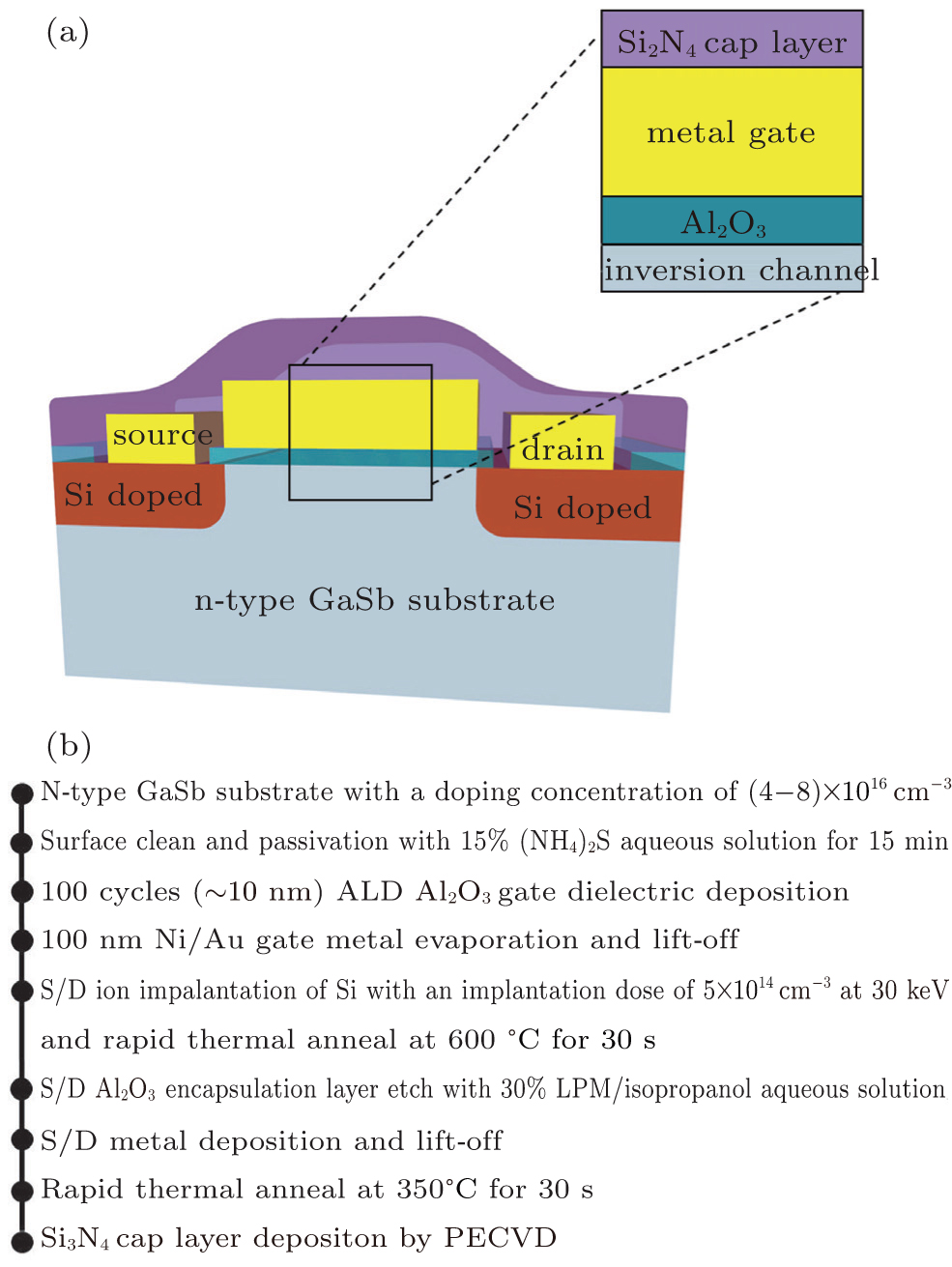
The MOSFETs, as shown in Fig. 1, were fabricated using a self-aligned gate-first process flow. Te-doped n-type GaSb (100)-oriented wafers with a doping concentration of (4–8)×1016 cm−3 were used as the starting substrates. The substrates were cleaned by sequential immersion in acetone, ethanol, and isopropanol for 5 min each, and in 9% HCl aqueous solution for 1 min, then passivated by 15% (NH4)2S aqueous solution for 15 min. After that, 100 cycles (∼10 nm) of ALD Al2O3 dielectric layer were deposited at 200 °C using a Beneq TFS 200 ALD system. Trimethylaluminum (TMA) and water were used as precursors. 100 nm Ni/Au gate metal was then evaporated and patterned using a lift-off process, which was followed by ion implantation of Si with an implantation dose of 5×1014 cm−2 at 30 keV for source/drain doping, which acts as the acceptor in GaSb.[13,22] Rapid thermal annealing (RTA) at 600 °C for 30 s was performed for dopant activation. After removing the Al2O3 encapsulation layer in the source/drain region by 30% KOH/isopropanol aqueous solution, the source and drain contacts were formed by Ni/Au deposition and lift-off. RTA at 350 °C for 30 s was performed to improve the source/drain metal contacts. An Si3N4 cap layer was finally deposited by PECVD to introduce a biaxial compressive strain. The amounts of the biaxial compressive strain determined by different growing conditions of the Si3N4 cap were 1.1%, 1.4%, and 2.0% respectively. The gate length of the fabricated GaSb MOSFETs was 2 μm. Characteristics were recorded using an Agilent B1500A semiconductor device analyzer and a Cascade Summit 11000 AP probe system.
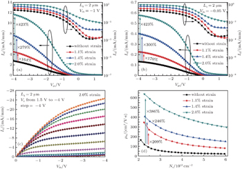
The experimental Id–Vg characteristics of various biaxial compressive strained GaSb p-channel MOSFETs with Vd at −1 V and −0.05 V are shown in Figs. 2(a) and 2(b), respectively. All our experimental results are obtained at room temperature. The biaxial compressive strained samples show a significant increase in the drain current compared with the unstrained ones. An on-state (Ion) to off-state (Ioff) current ratio Ion/Ioff as large as ∼ 2526 is obtained from the Id–Vg characteristics for the samples with 1.1% strain when Vds = −1 V, which is increased by 27.6% in comparison to the control samples without strain. The subthreshold swing (SS) of the device with 1.1% biaxial compressive strain is determined to be ∼568 mV/dec, which is similar to ∼573 mV/dec for the samples without strain. The SS measured at Vds = −50 mV is relatively large because of a large area of the source/drain regions in the device geometry, leading to a large off-state leakage current from the reverse-bias pn junction of the drain/substrate, which is not controlled by the gate voltage.[23] As the biaxial compressive strain increases, Ion/Ioff is decreased due to the increase of Ioff, which results from the change of the band-gap induced by the biaxial compressive strain (discussed in the next section in detail). The Ion is also increased in the samples with higher biaxial compressive strains. The peak drain current is 12 mA/mm when the gate bias is −4 V and the drain bias is −1 V with a 2.0% biaxial compressive strain, which shows a 4.23-fold increase when compared with that of the samples without strain.
Fig. 1. (a) Schematic diagram of biaxial compressive strained GaSb MOSFETs. (b) Process flow of self-aligned GaSb channel MOSFETs.
The experimental Id–Vd characteristics of 2.0% biaxial compressive strained GaSb p-channel MOSFETs with gate voltages ranging from 1.5 V to −4 V are illustrated in Fig. 2(c). The drain current increases in single steps with respect to the gate voltage and the drain bias, respectively. The drain current Id reaches its maximum of 24.6 mA/mm when the gate bias and the drain bias are both −4.0 V.
The hole mobility is extracted using a split-CV analysis based on the Id–Vg characteristics of the devices with various biaxial compressive strains, as shown in Fig. 2(d). It should be noted that no corrections for the source/drain resistance or any other corrections are applied while extracting the mobility. With a 2.0% biaxial compressive strain, the maximum hole mobility of 638 cm2/V·s is obtained, which is higher than that of the reference samples in this work and other published results.[13,22,24,25]
Fig. 2. The Id–Vg characteristics of various biaxial compressive strained GaSb p-channel MOSFETs with Vd at (a) −1 V and (b) −0.05 V. (c) The Id–Vd characteristics of 2.0% biaxial compressive strained GaSb p-channel MOSFETs with different gate voltages range from 1.5 V to −4 V. (d) Hole mobility enhancement characteristics.
3. First principles calculations
It is widely known that the effective mass is a key factor that determines the carrier mobility. To understand the physical origin of the enhancement of mobility, we next turn to study the the effective mass of GaSb under different biaxial compressive strains using first principles calculations.
Our calculations are performed using density functional theory (DFT) as implemented in the Vienna ab initio simulation package (VASP).[26] We use the projector augmented wave (PAW) method, with the exchange–correlation potential described by local density approximation (LDA). The energy cut-off is set at 400 eV. We use Monkhorst–Pack k-point meshes of 9×9×9. All the structures are relaxed until the residual forces on each atom are no more than 0.01 eV/Å. The spin–orbital interactions are considered in the structural relaxation as well as in the electronic structure calculations.
Crystalline GaSb has a zinc-blende structure, belonging to the space group in the Hermann–Mauguin notation, or in the Schoenflies notation.[27] Every Ga atom in the zinc-blende structure has four tetrahedral Sb neighbors. The experimental lattice constant of GaSb (6.10 Å) is used as the equilibrium lattice constant. To simulate the 1.1%, 1.4%, and 2.0% biaxial compressive strains applied on the GaSb sample, the lattice constants in the corresponding directions are reduced by 1.1%, 1.4%, and 2.0%, respectively. The carrier effective mass is obtained from the conduction and valance bands of GaSb with
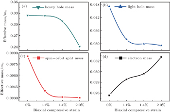
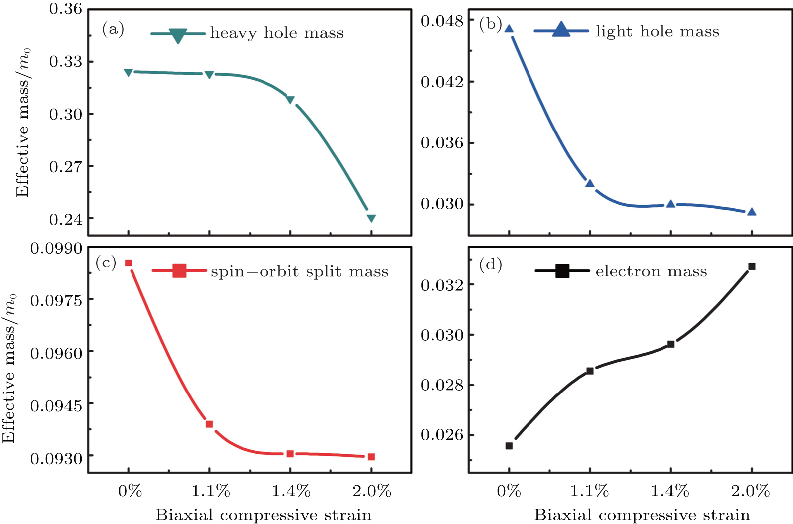
The calculated effective masses of holes and electrons are shown in Fig. 3. It is clear that as the biaxial compressive strain increases, the effective mass of holes decreases, while that of electrons increases. For example, as the biaxial compressive strain increases from 0 to 2%, the effective mass of the heavy hole decreases from 0.32 to 0.24, while that of the electron increases from 0.026 to 0.033.
For semiconductors, the smaller the effective mass, the higher the carrier mobility.[28] Obviously, the dramatic decrease of the hole effective mass of GaSb under biaxial compressive strain will result in the significant enhancement of the hole mobility, which agrees well with the experimental finding. Although the interface roughness also plays a vital role in carrier scattering and thus mobility,[29–31] the surface roughness of our GaSb substrates is carefully controlled and all of the samples have similar surface roughness, so we believe that the mobility enhancement is mostly due to the decrease of the hole effective mass.
Fig. 3. Carrier effective mass as a function of the biaxial compressive strain for the (a) heavy hole band, (b) light hole band, (c) spin–orbit split band, and (d) electron band. The calculated effective mass is in units of the free electron mass.
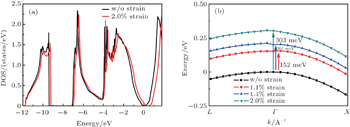
Fig. 4. (a) Density of states with and without 2% biaxial compressive strain. (b) Modulation of the valence band maximum.
The reduction of the hole effective mass is attributed to the strain-induced modulation of the valence band, which is verified by the calculated electronic structure of GaSb. The calculated densities of states (DOS) before and after inducing 2.0% biaxial compressive strain are illustrated in Fig. 4(a). For comparison, we have shifted the density of states of the strained GaSb by a small amount, so that the lower edges of the valence band DOS of the samples with and without strain match.[32] The density of states of the strained GaSb is significantly different in the vicinity of the energy gap position, compared with that of the unstrained GaSb. The valence band maximum (VBM) of GaSb after inducing 2.0% biaxial compressive strain shifts to a high energy position. The E–k relationship from the first principles calculations verifies the modulation of the VBM. As shown in Fig. 4(b), the VBM position shifts up by 152 meV, 201 meV, and 303 meV for 1.1%, 1.4%, and 2.0% biaxial compressive strains, respectively. Besides the shift of the VBM, the calculated electronic structure also shows that the valence band of the strained GaSb is steeper compared with that of the control sample without strain, which verifies the reduction of the hole effective mass due to the biaxial compressive strain.
4. Conclusion
We have studied various biaxial compressive strained GaSb p-channel MOSFETs both experimentally and theoretically. The biaxial compressive strain results in the reduction of the hole effective mass by the modulation of the valence band, thus enhancing the hole mobility of GaSb. Our experimental and theoretical work makes it possible to fabricate high performance GaSb p-channel MOSFETs.


 , Tan Zhen2, †,