1. IntroductionMetamorphic materials can be used as virtual substrates to reduce cost and they would be useful for many technological applications, such as field effect transistors (FET), lasers, high electron mobility transistors (HEMT), and multi-junction solar cells.[1–5] In general, threading dislocations which reduce the minority carrier lifetime are seen as the most important defect in metamorphic materials and are often used to evaluate the quality of the materials.
However, in zincblende crystals, two types of dislocations, i.e., α and β dislocations, which have [-110] and [110] line directions at compressively strained interfaces with As- and Ga- terminated cores, respectively, are introduced when the layer thickness is beyond the critical thickness. The orthogonal directions are not equivalent, which affects the uniformity of the strain relaxation and the dislocation density because of the significant differences in activation energies for α and β dislocation nucleation and glide. It has been found experimentally that α dislocations have a higher glide velocity than β dislocations in undoped and n-type GaAs.[6,7] Thus, the α dislocations are often reported to form preferentially during strain relaxation at InGaAs/GaAs interfaces.[8] Suzuki et al. have proved this anisotropy caused by α and β dislocations in relaxation processes using real-time three-dimensional reciprocal space mapping (3D-RSM) during I0.12Ga0.88As/GaAs (001) molecular beam epitaxial growth.[9] The asymmetry in dislocation densities, surface morphology, and strain relaxation of lnGaAs epilayers lattice mismatched to GaAs can be affected by the substrate orientation, V/III ratio, and growth temperature.[10,11] These asymmetric properties which cause anisotropic electron transport in metamorphic materials have a significant impact on the device performance.[12,13] So control over these growth parameters is very important for relaxation with the lowest dislocation density, and also allows the creation of devices with symmetric properties. Thus many researchers have investigated the mechanism of asymmetries in InGaAs layers grown on misoriented GaAs (001) substrates.[14–16] France et al. studied the asymmetric strain relaxation in InGaAs by an in situ multibeam optical stress sensor (MOSS) through controlling the growth temperature and V/III ratio.[11] Limited attention has been paid to InGaAs with symmetric properties. In this paper, we grew metamorphic In0.27Ga0.73As epilayers with symmetric low threading dislocation density and symmetric strain relaxation in two 〈110〉 directions using InAlGaAs buffer layers on 7° misoriented GaAs (001) substrates. In order to understand the control mechanism of the symmetric properties of the In0.27Ga0.73As layers by substrate miscut angles, In0.27Ga0.73As grown on 2° and 15° misoriented substrates were also characterized as reference by atomic force microscopy, transmission electron microscopy, and high resolution triple axis x-ray diffraction. Photoluminescence (PL) results reveal that In0.27Ga0.73As grown on 7° misoriented GaAs substrate has the best crystal quality compared with that grown on 2° and 15° misoriented GaAs substrates.
2. ExperimentsThe In0.27Ga0.73As epilayers of 1 μm thick were grown on Si-doped GaAs (001) substrates misoriented 2°, 7°, and 15° toward (111)A by metal organic chemical vapor deposition (MOCVD). For simplicity, the In0.27Ga0.73As epilayers grown on 2°, 7°, and 15° offcut GaAs substrates are referred to as 2°-off sample, 7°-off sample, and 15°-off sample, respectively. The growth temperature and V/III ratio were kept at 675 °C and 70, respectively. The nominal threading dislocation density of the substrates is below 500 cm−2 determined by the etch-pit density. The compositionally step-graded InxAlyGa1 − x − yAs buffer layer was used to gradually change the lattice constant while relaxing the strain. It consisted of eight 200 nm step-graded InxAlyGa1 − x − yAs layers with a constant band gap and a 1 μm reverse buffer layer.
Surface morphology and roughness of the samples were characterized by optical microscopy and atomic force microscopy (AFM). Misfit dislocations and threading dislocations in the samples were investigated by a Tecnai-G2-F20 transmission electron microscopy (TEM) working at 200 kV in the two-beam diffraction conditions. Strain relaxation rates and tilts of the samples were determined using two sets of reciprocal space mappings (RSMs), i.e., symmetric (004) and asymmetric (-2-24), which were measured in the two orthogonal [110] and [1-10] directions by high resolution triple axis x-ray diffraction using a Bruker D8 system. A (001) film can have either edge TDs or screw TDs with [001] line direction. Edge dislocations distort only the (hkl) planes with either h or k nonzero, while screw TDs with [001] line direction have a pure shear strain field that distorts all (hkl) planes with l nonzero.[17,18] So we used half maximum widths of the symmetric (004) rocking curve and the skew symmetric (115) rocking curve to characterize the density of TDs and the quality of the epilayers. Photoluminescence (PL) measurements were performed using an RPM 2000 mapping system with a 980 nm excitation laser.
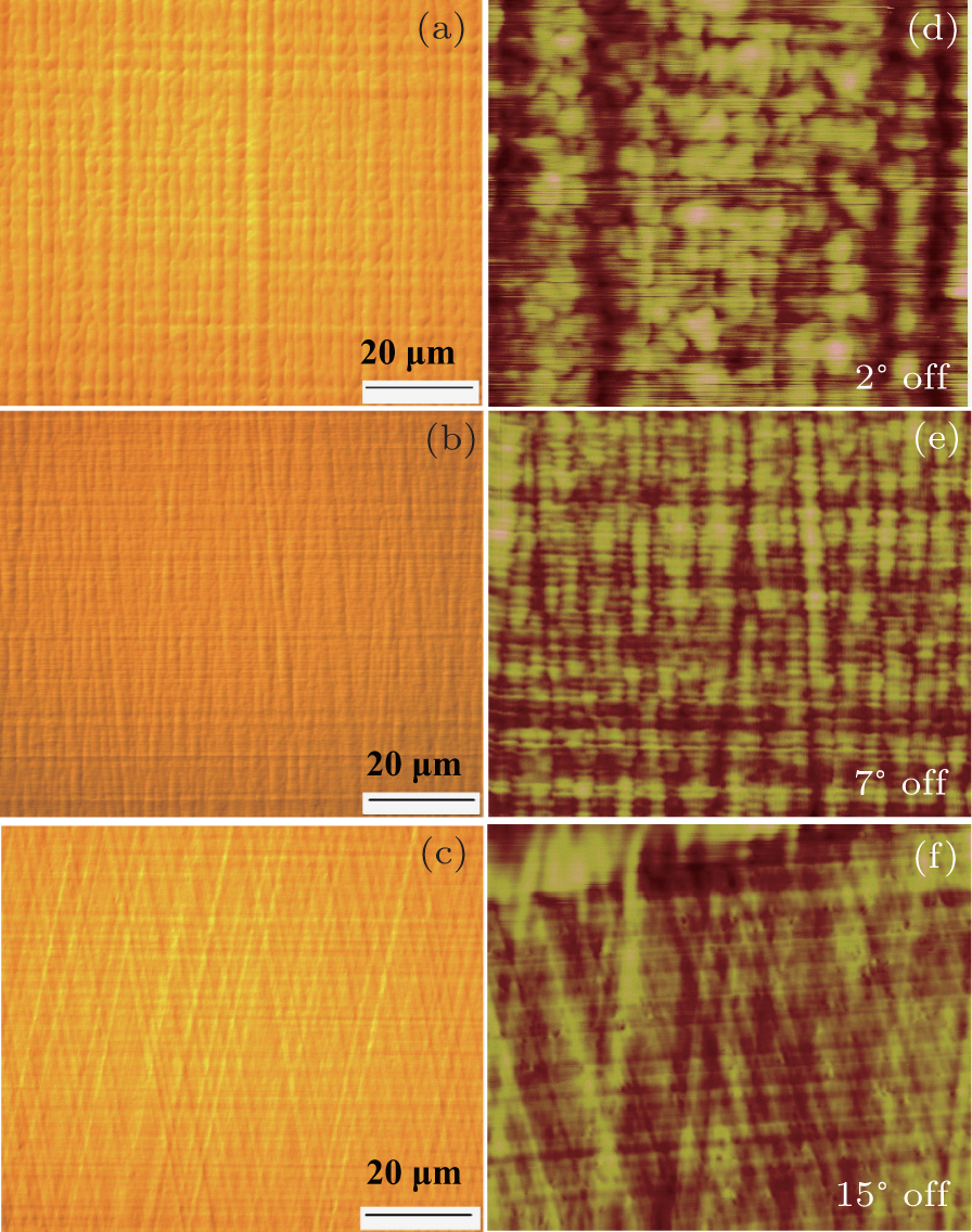
3. Results and discussionThe optical microscopic and AFM images of 2°-off, 7°-off, and 15°-off samples are shown in Fig. 1. The morphology of these samples displays a well-developed cross-hatched pattern with elongated hills and valleys, which is the typical surface morphology of relaxed compressively strained films with lattice mismatch less than 2%. Furthermore, angles between the elongated hills or valleys roughly aligned along the substrate miscut direction can be observed in all samples, and the measured angles are about 1.5°, 9°, and 20° for 2°-off, 7°-off, and 15°-off samples, respectively. AFM surface images of 40 μm × 40 μm are shown in Figs. 1(d)–1(f). The root-mean-square (RMS) roughness of the 2°-off sample is 7.24 nm in contrast to 5.21 nm and 5.59 nm of the 7°-off and 15°-off samples, respectively. Lots of pits can be seen in Fig. 1(f), indicating a high threading dislocation density in the 15°-off sample.
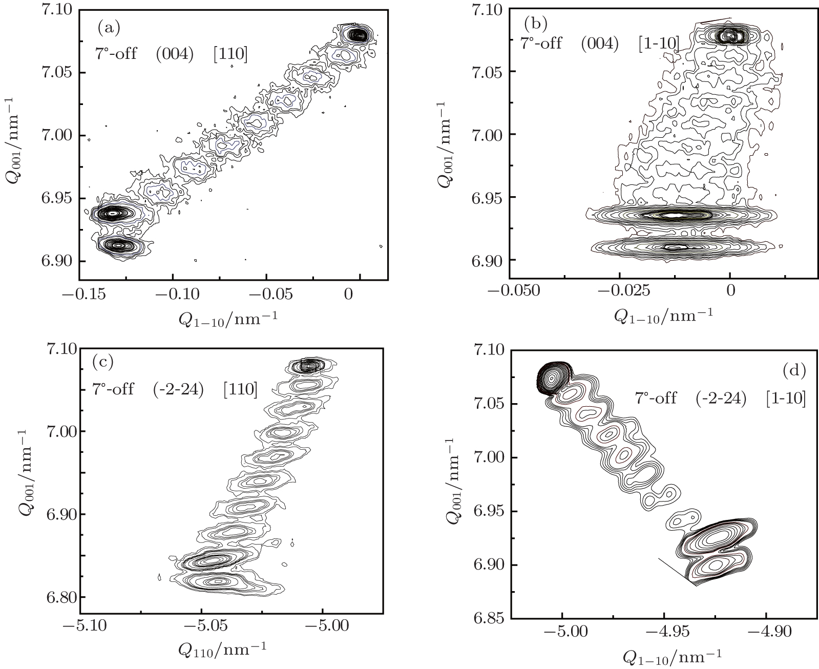
Figures 2(a) and 2(b) show the symmetric (004) RSMs of the 7°-off sample with the incident beam along the [110] and [1-10] directions, respectively. It is found that each layer has a crystallographic tilt with respect to the substrate along the [110] direction, while little tilt occurs between the epilayers and the substrate along the [1-10] direction, which can be neglected considering the experimental errors.[10] Figures 2(c) and 2(d) show the asymmetric (-2-24) RSMs of the 7°-off sample with the incident beam along the [110] and [1-10] directions, respectively. The tilts of the epilayer strongly affect the peak positions in both the (004) and (-2-24) RSMs. Therefore, the tilts must be taken into account for an accurate calculation of the strain relaxation rate in the In0.27Ga0.73As layers. The tilts and relaxation rates of the top In0.27Ga0.73As layers grown on the 2°-off, 7°-off, and 15°-off cut substrates are listed in Table 1.
Table 1.
Table 1.
 Table 1. Relaxation rates, tilts, widths of 2θ scan curves of (-2-24) RSMs, (004) and (115) rocking curve widths along [110] and [1-10] directions of the 2°-off, 7°-off, and 15°-off samples. .
| Substrate miscut |
Relaxation/% |
Tilt/(°) |
(-2-24) 2θ /ω width/arcsec |
(004) symmetric width/arcsec |
(115) skew symmetric width/arcsec |
|
[110] |
[1-10] |
[110] |
[1-10] |
[110] |
[1-10] |
[110] |
[1-10] |
[110] |
[1-10] |
| 2°-off |
86.5 |
90.7 |
0.78 |
0.02 |
455 |
552 |
1519 |
820 |
1448 |
690 |
| 7°-off |
95.5 |
96.2 |
1.09 |
0.02 |
243 |
328 |
266 |
274 |
263 |
266 |
| 15°-off |
97.2 |
96.7 |
0.74 |
0.02 |
280 |
254 |
293 |
879 |
298 |
923 |
| Table 1. Relaxation rates, tilts, widths of 2θ scan curves of (-2-24) RSMs, (004) and (115) rocking curve widths along [110] and [1-10] directions of the 2°-off, 7°-off, and 15°-off samples. . |
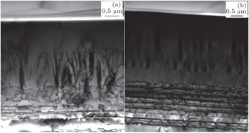
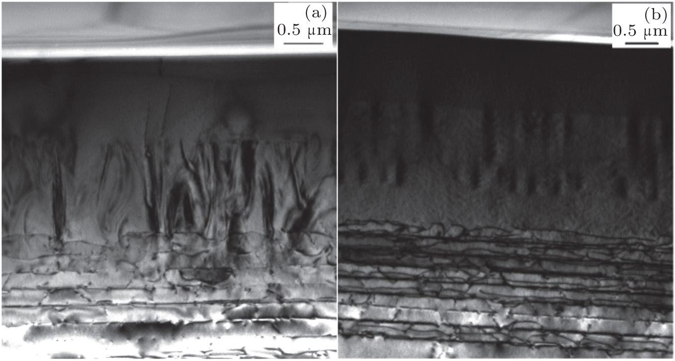
The (-2-24) RSMs of the In0.27Ga0.73As show a significantly greater spread in the 2θ direction, i.e., 455 arcsec in the [110] direction, while 552 arcsec in the [1-10] direction for the 2°-off sample compared to those for the 7°-off and 15°-off samples (widths: 243-328 arcsec) in Table 1. This larger spread indicates a wide distribution of the lattice constant or indium composition, which is consistent with a phase separation.[19] This is proven by XTEM analysis shown in Figs. 3(a) and 3(b). In the 2°-off sample, many misfit dislocations (MDs) are trapped by the phase separation, which produces diffraction contrast features, so they stop gliding and turn upwards and thread to the next buffer layer, some of them even propogate to the In0.27Ga0.73As layer. While the phase separation is much weaker in the 7°-off sample, so the MDs glide with less resistance on the plane parallel to the image plane and appear as long and smooth lines, and consequently no TDs are observed in the In0.27Ga0.73As XTEM image. This consists with the results shown in Table 1 that the widths of the (004) and (115) rocking curves for the 2°-off sample are 690–1500 arcsecond in the two 〈110〉 directions, but about 265 arcsecond for the 7°-off sample in the two 〈110〉 directions.
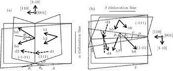
For compressively strained metamorphic epilayers, one of the strain relaxation mechanisms is the nucleation and glide of 60° a/2〈110〉 {111} MDs, the other is the nucleation and glide of 30° and 90° Shockley partial MDs.[20] When the substrate miscut angle increases, the nucleation and glide of 90° MDs should be taken into account, because the nucleation energy for a 90° MD is much lower than that for a 60° MD.[21,22] 60° MDs can nucleate on four {111} glide planes with two possible Burgers vectors on each glide plane, resulting in eight glide systems in total denoted as b1–b8 in Fig. 4, while only one possible glide system for 90° MDs can be formed on each glide plane, denoted as d1–d4.
For a given glide system, the shear stress due to the misfit strain resolved in the glide direction on the glide plane serves as a driving force, given as Fg = σ bsinθ cosθ cosΦ± γsf for dislocation gliding,[21–23] where σ is the biaxial stress in the interface, b is the Burgers vector, θ is the angle between the glide plane and the interface, Φ is the angle between the Burgers vector and the direction in the glide plane which is normal to the intersection of the glide plane and the interface, sin θ cos θ cosΦ is the Schmid factor which is proportional to the shear stress, γsf is the stacking fault energy, and the sign before γsf is positive or negative when a stacking fault is removed or created during the nucleation of a partial dislocation, respectively. The activation energy for dislocation nucleation is inversely proportional to the shear stress, while the dislocation glide velocity is proportional to the shear stress, thus the glide system with the greatest Schmid factor is expected to dominate both the nucleation and glide processes.[10,22] Both θ and Φ depend on the substrate miscut angle, and therefore dislocations in each individual glide system experience different glide forces since their Schmid factors sin θ cos θ cosΦ are different for both 60° and 90° MDs, as shown in Fig. 5.
For the 2°-off sample, the Schmid factors of the 60° α and β MDs are the same, while the Schmid factor of the 90° α MDs is slightly larger than that of the 90° β MDs. Meanwhile, for growth of InGaAs on GaAs substrate, the α MDs have lower formation energy and higher glide velocity compared with the β MDs and are formed prior to the β MDs.[7,11] Thus more α MDs may nucleate at each interface layer in the [1-10] direction in the 2°-off sample. However, the phase separation which tends to resist gliding of MDs is stronger in the [1-10] direction than that in the [110] direction, resulting in more threading dislocations in the [1-10] direction but a lower relaxation rate in the [110] direction in the 2°-off sample. Consequently, the rocking curve widths of the 2°-off sample in the [110] direction are larger than those in the [1-10] direction for both the (004) and (115) diffractions. This also indicates that the strain relaxation process in the metamorphic epilayers is dominated by the dislocation glide rather than the dislocation nucleation. So the relaxation rates of the 7°-off and 15°-off samples in the two 〈110〉 directions are almost the same and are larger than that of the 2°-off sample, which are all consistent with the 2θ widths of the (-2-24) RSMs of the samples shown in the Table 1.
For the 7°-off sample, the Schmid factors of 60° β MDs and 90° α MDs are increased, thus the nucleation and glide of 60° β MDs and 90° α MDs are enhanced. The widths of the (004) and (115) rocking curves in the [110] direction are as narrow as those in the [1-10] direction in the 7°-off sample. This indicates that the weak phase separation in the [1-10] direction does not increase the threading dislocation density. When the substrate miscut angle is increased from 7° to 15°, the Schmid factor of the 60° β MDs is greatly increased. Furthermore, the angle between two 60° MDs lines in the substrate miscut direction is increased from 9.86° to 20.77° for the 7°-off and 15°-off samples, respectively, as shown in Fig. 1(f). So the chances of nucleation of new complementary 60° β MDs and the intersection of two already existing complementary 60° β MDs increase. As a result, the Y type 90° β MDs are greatly increased, and the misfit dislocation lines become shorter.[24,25] For a single mismatched layer, the average misfit dislocation glide length is related to ρt and ρm as[26]

where
L is the width of the sample,
ρm is the sum of the misfit dislocation density throughout the total thickness of the graded buffer layer and the top layer which involve many interfaces,
ρt is the threading dislocations, and 〈
l〉 is the average misfit glide length. So we can qualitatively conclude that
ρt is higher in the larger substrate miscut sample in the substrate miscut direction due to the shorter 〈
l〉 and the higher
ρm. Consequently, the widths of the (004) and (115) rocking curves (about 293 arcsecond) in the [110] direction of the 15°-off sample are the same as those of the 7°-off sample, while it is increased to 923 arcsecond in the [1-10] direction.
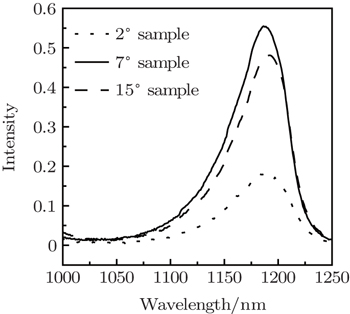
Figure 6 shows the room temperature PL spectra of In0.27Ga0.73As layers in the 2°-off, 7°-off, and 15°-off samples. The PL peak intensity of the 7°-off sample is obviously the strongest among the three samples, suggesting a lower density of threading dislocations acting as nonradiative recombination centers in the In0.27Ga0.73As layer.


 , Sun Yu-Run1, Li Kui-Long1, 2, Zeng Xu-Lu1, 2, Zhao Yong-Ming1, Yang Hui1]