Superior material qualities and transport properties of InGaN channel heterostructure grown by pulsed metal organic chemical vapor deposition
Zhang Ya-Chao , Zhou Xiao-Wei , Xu Sheng-Rui , Chen Da-Zheng , Wang Zhi-Zhe , Wang Xing , Zhang Jin-Feng , Zhang Jin-Cheng , Hao Yue
State Key Discipline Laboratory of Wide Band Gap Semiconductor Technology, School of Microelectronics, Xidian University, Xi’an 710071, China


† Corresponding author. E-mail: jchzhang@xidian.edu.cn

Project supported by the National Natural Science Foundation of China (Grant Nos. 61306017, 61334002, 61474086, and 11435010) and the Young Scientists Fund of the National Natural Science Foundation of China (Grant No. 61306017).

Abstract
Abstract

Pulsed metal organic chemical vapor deposition is introduced into the growth of InGaN channel heterostructure for improving material qualities and transport properties. High-resolution transmission electron microscopy imaging shows the phase separation free InGaN channel with smooth and abrupt interface. A very high two-dimensional electron gas density of approximately 1.85 × 10 13 cm −2 is obtained due to the superior carrier confinement. In addition, the Hall mobility reaches 967 cm 2 /V·s, owing to the suppression of interface roughness scattering. Furthermore, temperature-dependent Hall measurement results show that InGaN channel heterostructure possesses a steady two-dimensional electron gas density over the tested temperature range, and has superior transport properties at elevated temperatures compared with the traditional GaN channel heterostructure. The gratifying results imply that InGaN channel heterostructure grown by pulsed metal organic chemical vapor deposition is a promising candidate for microwave power devices.

1. Introduction

The application of AlGaN/GaN heterostructures in fabricating high electron mobility transistors (HEMTs) has received much attention since 1993 because of their outstanding electrical properties. [ 1 3 ] So far the studies have entered into a more mature stage, and the research effort is shifting to the higher frequency microwave power device. [ 4 ] However, there are still some limitations of the GaN-based HEMTs, such as the low-frequency 1/ f noise and the RF-current collapse, which are attributed to the inferior confinement of the highdensity two-dimensional electron gas (2DEG) in channel. [ 5 ] To address this limitation and spatially confine the channel electrons, InGaN channel is proposed as a substitute for the traditional GaN channel. In comparison with GaN, InGaN channel has a narrower band gap and forms a deeper quantum well with a wide band gap barrier. [ 6 , 7 ] On the other hand, due to the large electron affinity of InN (5.8 eV), [ 8 ] the In- GaN channel forms a large discontinuity of conduction band at the interface between InGaN channel and GaN buffer layers. Hence the employment of the InGaN channel effectively increases the carrier confinement in the channel layer. As a consequence, the InGaN channel heterostructure shows better performances in suppressing the 1/ f noise [ 9 ] and RF-current collapse [ 5 , 10 ] than the GaN channel. [ 11 ] In addition, the InGaN channel is theoretically superior to the conventional GaN channel in such aspects as the higher saturation velocity and sheet carrier density attainable, [ 12 ] which are beneficial to the improvement of 2DEG mobility and density. [ 13 ] Furthermore, according to the previous research, HEMT with InGaN channel operates well in suppressing the virtual gate effect. [ 14 ] Therefore, InGaN channel heterostructures have a great potential in fabricating microwave power devices.

Some achievements have been obtained in demonstrating the outstanding properties of InGaN channel heterostructures and devices. [ 15 18 ] However, from the epitaxial point of view, it is still a challenge to obtain high-quality InGaN channel according to the state-of-the-art epitaxial technology. The main issues are the phase separation [ 19 ] and composition inhomogeneity, resulting from unfavorable thermodynamic reactions. In this paper, pulsed metal organic chemical vapor deposition (PMOCVD) is used to grow InGaN channel, and satisfactory material qualities and heterostructure properties are obtained. The microstructure of InAlN/InGaN heterostructure grown by PMOCVD is detected by high-resolution transmission electron microscopy (HR-TEM). The HR-TEM image shows the phase-separation-free InGaN channel with smooth and abrupt interface, indicating the superiority of PMOCVD and well-controlled growth technology in our experiments. Besides, according to the fact that little attention has been paid to the transport properties of InGaN channel heterostructures at high temperature, temperature-dependent Hall measurement is also carried out, and the results show the InGaN channel heterostructure is superior compared with the conventional GaN channel heterostructure at elevated temperatures.

2. Experimental procedure

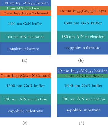
The samples investigated in this paper were grown on the two-inch c -plane sapphire substrates in a home-made vertical low pressure metal organic chemical vapor deposition (MOCVD) system. The sectional view of the InAlN/InGaN heterostructure sample is shown in Fig. 1(a) . Firstly, 20-nm-thick low temperature AlN nucleation layer and 160 nm high-temperature AlN nucleation layer were deposited on the sapphire substrate successively. Their growth temperatures were 620 °C and 1070 °C. Then, 1600 nm nominally undoped GaN buffer was grown at 940 °C. Afterwards, the carrier gas was switched from hydrogen to nitrogen, and the growth temperature dropped to 720 °C. A 7-nm InGaN channel layer was deposited followed by a 1-nm AlN interlayer. Finally, 19-nm InAlN barrier layer was grown. According to the previous report, the application of pulsed growth mode has a positive influence on the material qualities of InN, which is attributed to the better surface mobility of indium adatoms. [ 20 ] The method of PMOCVD was introduced into the growth of InGaN channel in our experiments. The growth sequence of unit cells for InGaN channel is shown in Fig. 2 . As can be seen, the unit pulses of 6-second TEGa, 6-second NH 3 , and 12-second TMIn were introduced into the MOCVD reactor successively, and the metal organic pulses were always followed by the NH 3 pulses. That is to say, the growth process of the InGaN channel was divided into a serious of GaN/InN short period superlattice structures. This change in growth mode makes it easy to control the accurate thickness of the InGaN channel layer. The pulse cycle was repeated 40 times for InGaN channel layer.

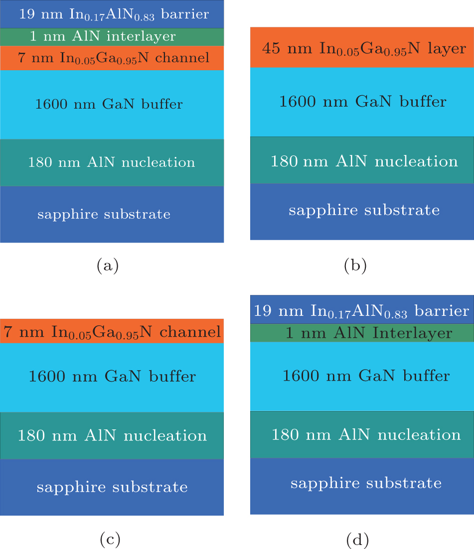
Fig. 1. Epilayer structures for (a) InAlN/InGaN heterostructure, (b) 45-nm InGaN layer, (c) 7-nm InGaN channel layer, (d) InAlN/GaN heterostructure grown by (pulsed) MOCVD.
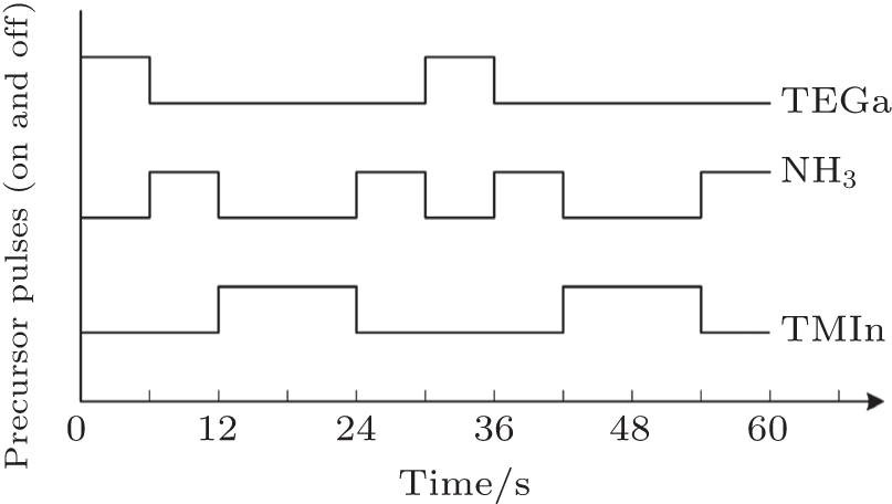
Fig. 2. Growth sequence of PMOCVD for InGaN channel layer.
3. Results and discussion

Figure 3(a) shows the cross-sectional TEM image of the entire epilayer structure as shown in Fig. 1(a) , which is taken near the [1-100] zone axis (under the two-beam bright field imaging condition). It can be seen that a great deal of dislocations exist in the AlN nucleation layer and at the bottom of the GaN buffer, which relates to the lattice mismatch stress relief. With the deposition of GaN buffer, the density of the dislocations reduced evidently, and only a very small quantity of dislocations extend into the top InAlN/InGaN heterojunction. In order to detect the detailed information about the top InAlN/InGaN heterojunction, HR-TEM image with a higher magnification of the InAlN/InGaN heterostructure is shown in Fig. 3(b) . Abrupt and smooth interfaces between the GaN buffer, InGaN channel and InAlN barrier layers can be clearly observed. The thickness of the InGaN channel and InAlN barrier are 7 nm and 19 nm, respectively. Unlike the previous result, [ 21 ] there is no obvious phase separation nor threading dislocation in the InGaN channel layer. The result indicates that the growth procedure in our experiment is well-controlled and the application of PMOCVD significantly improves the material qualities and uniformity of the InGaN channel layer. As a consequence, the high-quality InGaN channel will be helpful to improve the transport properties of heterostructure.

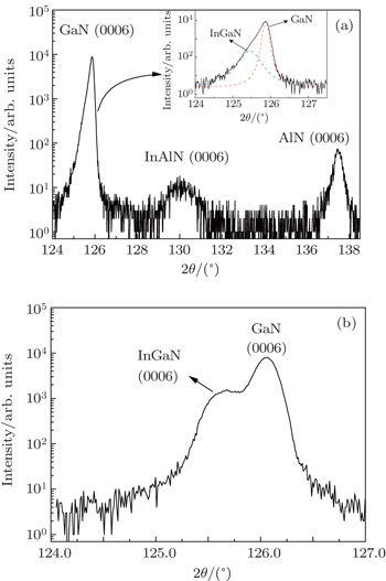
The typical high-resolution x-ray diffraction (HR-XRD) ω −2 θ scan of the InAlN/InGaN heterostructure from the symmetric (0 0 0 6) reflection is shown in Fig. 4(a) . The diffraction curve is dominated by three peaks located at 126.0°, 130.3°, and 137.3°, which correspond to the GaN buffer, InAlN barrier, and AlN nucleation layer, respectively. Like the result in a previous report, [ 22 ] the InGaN channel is much thinner than other layers and no distinct diffraction peak for it can be observed. However, as shown in the magnifying spectrum scan from 124° to 127.5° in the inset, there is an obvious slope at the small angle side of the GaN main peak, which is due to the diffraction of InGaN channel. The Lorentz fitted result shows two distinct peaks corresponding to InGaN and GaN, respectively. This phenomenon was not observed in the previously reported result with even thicker InGaN channel. [ 23 ] Taking the layer thickness of 7 nm into consideration, the XRD results demonstrate the high diffraction intensity of the InGaN channel layer, suggesting the favorable material quality of InGaN grown by PMOCVD. Furthermore, in order to judge the accurate indium composition in the InGaN channel, 45-nm-thick InGaN film on GaN buffer as shown in Fig. 1(b) is grown by PMOCVD under the identical conditions as that in the InGaN channel, and the HR-XRD scan of ω –2 θ from symmetric (0 0 0 6) reflection is shown in Fig. 4(b) (the spectrum scan from 124° to 127.5° is provided for clarity). Two unambiguous peaks corresponding to InGaN and GaN can be observed at 125.5° and 126° respectively, and they are in agreement with the Lorentz fitted results. Furthermore, it is noted that no peaks are observed except those corresponding to GaN, InGaN layers in the entire 2 θ range, suggesting that the InGaN film is grown pseudomorphically and strained on the GaN buffer layer without phase separation. The indium molar fraction, x , based on the chemical formula In x Ga 1− x N, can be determined from Vegard’s law (as shown in Eq. ( 1 )) based on the HR-XRD results [ 24 ]

where c InGaN , c GaN , and c InN are the actual c -plane lattice constants of InGaN, GaN, and InN, respectively. Finally, the indium molar fraction in InGaN channel is calculated to be about 5%.

Fig. 3. (a) Overview two-beam bright field cross-sectional TEM image of the entire epilayer sample, taken near the [1–100] zone axis. (b) High resolution TEM cross-sectional image of the top InAlN/InGaN heterostructure grown by PMOCVD.
Fig. 4. High-resolution XRD triple-axis (0 0 0 6) ω –2 θ scans of (a) InAlN/InGaN heterostructure and (b) 45-nm InGaN film on GaN buffer.

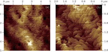
According to the previous studies, interface roughness scattering in InGaN channel heterostructures is more serious than those in conventional GaN channel samples, [ 25 ] which is the most acute issue that impedes the improvement of 2DEG mobility. In addition, interface roughness scattering becomes even more serious at room temperature. [ 26 , 27 ] Therefore, for improving the 2DEG mobility, it is of great importance to make a smooth interface in InGaN channel heterostructure. In order to detect the interface morphology between the InGaN channel and barrier layers in a straightforward way, an additional sample as shown Fig. 1(c) is also grown. The additional sample has a similar structure to the sample in Fig. 1(a) , but without the 19 nm InAlN barrier nor 1 nm AlN interlayer. Figure 5 shows the atomic force microscopy (AFM) surface images of the InGaN channel with scan areas of (a) 5 × 5 and (b) 2 × 2 μm 2 , respectively. As can be seen, the surface morphology of InGaN channel differs significantly from the previously reported result grown by the standard MOCVD process. [ 27 ] There is no crack nor trench on the smooth surface, and clear atomic steps can be seen. The flat surface is accompanied by small pits that are known as V defect, which is related to the surface termination of expanded dislocations generated in the GaN buffer. [ 28 ] The pit density is approximately 8.5 × 10 8 cm −2 in a 2 × 2 μm 2 scan area, indicating the high material quality of the InGaN channel with few regenerative dislocations. In addition, the root mean square (rms) surface roughness is measured to be as low as 0.26 nm for the 2 × 2 μm 2 scan area. This value is better than the result reported previously. [ 27 ] We attribute the improvement in surface morphology to the application of PMOCVD method. The reactive atoms are separately supplied to the reactor at different times. This growth mode enlarges the mobility of the adatoms and enables them to find energetically favorable sites. The improvement in interface morphology will be beneficial to the suppression of roughness scattering and also the improvement of carrier mobility.

Fig. 5. AFM images of surface morphology of InGaN channel with scan areas of (a) 5 × 5 and (b) 2 × 2 μm 2 .

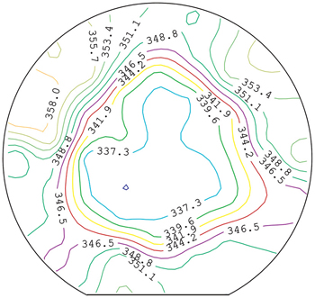
We first measure the transport properties of InAlN/InGaN heterostructure by room temperature (RT) Hall measurement. The 2DEG density reaches 1.85 × 10 13 cm −2 with an electron mobility of 967 cm 2 /V·s. Sheet resistance and resistance uniformity of the two-inch wafer are also measured by the contactless eddy current sheet resistivity mapping. As shown in Fig. 6 , the InAlN/InGaN sample presents resistance from 335.0 to 361.1 Ω/◻. The average sheet resistance is 346.7 Ω/◻ with a nonuniformity of 1.95%. The results are indicative of the high material quality and good uniformity of InGaN channel layer across the whole wafer. Therefore, InAlN/InGaN heterostructures grown by PMOCVD are promising candidates for microwave power devices.

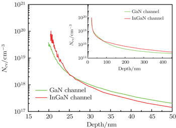
For additional electrical information, such as the sheet carrier concentration and 2DEG confined position, capacitance–voltage (CV) profiling technique is applied and operated at room temperature with a test frequency of 100 kHz and an Hg probe with a contact area of 600 μm 2 . For contrast, the result of conventional InAlN/GaN heterostructure as shown in Fig. 1(d) is also presented. As displayed in Fig. 7 , for the heterostructures with InGaN and GaN channel, the 2DEG peak density is located about 20 nm away from the surface, which offers hints towards a confinement close to the AlN/InGaN interface, considering the InAlN barrier thickness of 19 nm and AlN interlayer thickness of 1 nm. The peak carrier density in InGaN channel is 1.45 × 10 20 cm −3 , much higher than 0.39 × 10 20 cm −3 in the GaN channel. In addition, the carrier distribution in InGaN channel heterostructure is much steeper than that in GaN channel, implying that there is excellent carrier confinement in InGaN channel heterostructure. This improvement is attributed to the larger band offset between the InGaN channel and InAlN barrier layers and the good InGaN channel material quality grown by PMOCVD.

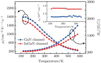
In order to meet the needs of different applications, HEMTs should operate steadily and reliably in a wide temperature range. The transport performances of InGaN channel heterostructures at low temperature and room temperature have been demonstrated. [ 22 , 23 , 26 ] For the further investigation of the 2DEG transport properties of InAlN/InGaN heterostructures in a wider temperature range, extended temperature-dependent (120–580 K) Hall measurement, conducted on a 1 cm × 1 cm sample in van der Pauw geometry using four indium dots as Ohmic contacts, is carried out. For contrast, the results of traditional InAlN/GaN heterostructure over the same temperature range are also shown. Figure 8 shows the temperature dependences of the Hall mobility ( μ ), sheet carrier density ( n s ), and sheet resistance ( R s ) of InAlN/InGaN, and traditional InAlN/GaN heterostructures. Both the heterostructures with InGaN and GaN channel show the typical 2DEG properties in the whole temperature range. At low temperature, the conventional GaN channel sample has higher electron mobility than the InGaN channel sample. We attribute the relatively high carrier mobility of the GaN channel sample to the absence of alloy disorder scattering from the ternary InGaN alloy compared with the InGaN channel sample. As the temperature increases, the carrier mobility in each sample decreases, owing to the enhanced influence of polar optical phonon scattering. [ 29 ] However, 2DEG mobility of GaN channel sample decreases more rapidly than the InGaN channel sample, and InGaN channel sample shows the better result when the temperature exceeds 400 K. On the other hand, the 2DEG density in InGaN channel sample is higher than that in the GaN channel sample in the whole temperature range. At elevated temperatures, the 2DEG density in GaN channel presents a fluctuation trend. We attribute the fluctuation to the inferior carrier confinement: the electrons possess higher energy at high temperature, and more easily spill out into the adjacent layers, [ 5 ] leading to an unstable 2DEG density in channel layer. However, for InGaN channel sample, the 2DEG density is stable in the whole temperature range due to the better carrier confinement. It is noteworthy that the R s value of InAlN/InGaN heterostructure is a little higher than that extracted from the sheet resistance mapping. It might be related to the modification of the potential of the bare InAlN barrier surface during the Ohmic contact electrode processing steps, and this deviation also appears in the GaN channel sample. In conclusion, it is speculated that the application of InGaN channel is promising to improve the transport properties of HEMTs, especially at elevated temperature.

Fig. 6. Sheet resistance mapping of 2-in InAlN/InGaN heterostructure wafer.
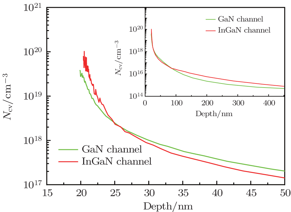
Fig. 7. Profiles of the carrier concentration as a function of the depth for InAlN/InGaN and InAlN/GaN heterostructures, measured by CV method.
Fig. 8. Variations of Hall mobility ( μ ), 2DEG density ( n s ), and sheet resistance ( R s ) for InAlN/InGaN and InAlN/GaN heterostructures with temperature.
4. Conclusions

In this work, PMOCVD is used to grow high-quality InGaN channel heterostructure, which is proven to be rewarding to the improvement of InGaN material quality, and further to the transport properties of heterostructure. The microstructure and satisfactory transport properties in this paper indicate that InGaN channel heterostructure grown by PMOCVD is a promising candidate for microwave power devices.

Reference
1 Khan M A Bhattarai A Kuznia J N Olson D T 1993 Appl. Phys. Lett. 63 1214
2 Mi M H Zhang K Zhao S L Wang C Zhang J C Ma X H Hao Y 2015 Chin. Phys. B 24 027303
3 Cao M Y Lu Y Wei J X Chen Y H Li W J Zheng J X Ma X H Hao Y 2014 Chin. Phys. B 23 087201
4 Chung J W Hoke W E Chumbes E M Palacios T 2010 IEEE Electron Device Lett. 31 195
5 Simin G Hu X Tarakji A Zhang J Koudymov A Saygi S Yang J Khan A Shur M S Gaska R 2001 Jpn. J. Appl. Phys. 40 L1142
6 Chu R M Zheng Y D Zhou Y G Gu S L Shen B Zhang R Jiang R L Han P Shi Y 2003 Appl. Phys. A 77 669
7 Okamoto N Hoshino K Hara N Takikawa M Arakawa Y 2004 J. Cryst. Growth 272 278
8 Ager lll J W Miller N Jones R E Yu K M Wu J Schaff W J Walukiewicz W 2008 Phys. Status Solidi B 245 873
9 Pala N Rumyantsev S Shur M Gaska R Hu X Yang J Simin G Khan M A 2003 Solid-State Electron 47 1099
10 Lanford W Kumar V Schwindt R Kuliev A Adesida I Dabiran A M Wowchak A M Chow P P Lee J W 2004 Electron. Lett. 40 771
11 Zhou X Y Feng Z H Wang Y G Gu G D Song X B Cai S J 2015 Chin. Phys. B 24 048503
12 Morkoc H 2008 Handbook of Nitride Semiconductors and Devices Vol. 3, GaN-based Optical and Electronic Devices New York Wiley 375
13 Maeda N Saitoh T Tsubaki K Nishida T Kobayashi N 1999 Jpn. J. Appl. Phys. 38 L799
14 Neuburger M Daumiller I Zimmermann T Kunze M Koley G Spencer M G Dadgar A Krtschil A Krost A Kohn E 2003 Electron. Lett. 39 1614
15 Hsin Y Hsu H Chuo C Chyi J 2001 IEEE Electron Device Lett. 22 501
16 Simin G Koudymov A Fatima H Zhang J Yang J Khan M A Hu X Tarakji A Gaska R Shur M S 2002 IEEE Electron Device Lett. 23 458
17 Adivarahan V Gaevski M Koudymov A Yang J Simin G Khan M A 2007 IEEE Electron Device Lett. 28 192
18 Sugita K Tanaka M Sasamoto K Bhuiyan A G Hashimoto A Yamamoto A 2011 J. Cryst. Growth 318 505
19 Wang Q Ji Z W Wang F Mu Q Zheng Y J Xu X G Y J Feng Z H 2015 Chin. Phys. B 24 024219
20 Johnson M C Konsek S L Zettl A Bourret-Courchesne E D 2004 J. Cryst. Growth 272 400
21 Ruterana P Aguinet R Poisson M A 1999 Phys. Status Solidi B 216 663
22 Ikki H Isobe Y Iida D Iwaya M Takeuchi T Kamiyama S Akasaki I Amano H Bandoh A Udagawa T 2011 Phys. Status Solidi A 208 1614
23 Gökden S Tülek R Teke A Leach J H Fan Q Xie J Özgür Ü Morkoç H Lisesivdin S B Özbay E 2010 Semicond. Sci. Technol. 25 045024
24 Beh K P Yam F K Chin C W Tneh S S Hassan Z 2010 J. Alloys Compd. 506 343
25 Wang C X Tsubaki K Kobayashi N Makimoto T Maeda N 2004 Appl. Phys. Lett. 84 2313
26 Xie J Leach J H Ni X Wu M Shimada R Özgür Ü Morkoç H 2007 Appl. Phys. Lett. 91 262102
27 Laboutin O Cao Y Johnson W Wang R Li G 2012 Appl. Phys. Lett. 100 121909
28 Romano L T Krusor B S McCluskey M D Bour D P Nauka K 1998 Appl. Phys. Lett. 73 1757
29 Yu T H Brennan K F 2001 J. Appl. Phys. 89 3827