1. Introduction More and more attention has been paid to AlGaN/GaN HEMTs due to their superiorities of high breakdown electric field and high electron saturation velocity as well as high carrier density for RF power and power electronics applications. [ 1 – 4 ] Recently, the actual demands of good reserve blocking capability in power converters, [ 5 ] class-S amplifier, [ 6 ] power management systems, [ 7 – 9 ] and so on, have been one of the most important catalysts for studies of various kinds of Schottky drain (SD) in AlGaN/GaN HEMTs (SD HEMTs). [ 10 – 14 ] These studies revealed that the improvement of reserve blocking capability with SD is mainly attributed to the formation of the depletion region around the drain, effectively suppressing the buffer leakage. However, the ability of SD to enhance the reverse breakdown voltage V BR is limited because of its limited depletion region under reverse bias. Field plates (FPs), widely used in AlGaN/GaN HEMTs to improve the forward blocking capability, [ 15 – 19 ] could be promising techniques with great potential in SD HEMTs. A significant increase in reverse breakdown voltage for SD HEMTs by means of a drain FP (DFP) has been observed. [ 20 ] Nevertheless, similar to the FP in the forward blocking applications, the DFP may suffer the same troubles of the decreasing breakdown voltage increment with the increasing FP length in the reverse blocking applications. [ 16 , 21 ] Multiple FPs [ 18 ] may be a possible technique to solve this trouble by continually increasing the number of FPs. Unfortunately, the more FPs we use in multiple FPs HEMT, the more complex the device fabrication will be. Thus, much more effective FP structures deserve to be explored so as to further improve the reverse blocking capability.
In this paper, a novel SD HEMT with a compound FP (CFP) is proposed for the purpose of better reverse blocking enhancement. The proposed CFP is composed of a DFP and several floating field plates (FFPs) based on the inspiration from field-limiting rings. [ 22 ] The simulations of physical mechanism in SD HEMT with a CFP (SD-CFP HEMT), relating to the improvement of the reverse blocking capability together with the CFP modulation effects on the channel electric field and potential distributions, are investigated in detail by Silvaco-ATLAS. Moreover, the optimization methods containing two key and useful laws, and the relationship between the number of the FFPs and the reverse breakdown voltage as well as the FP efficiency in SD-CFP HEMTs are achieved based on our simulation results. These results above are of great value for the design and actual manufacture processes of SD-CFP HEMTs.
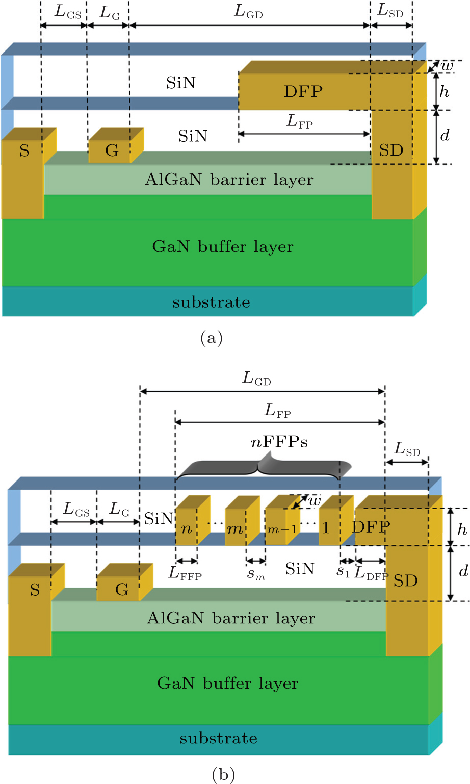
2. Device structures and simulation models Figure 1 shows the schematics of SD-FP HEMT and SD-CFP HEMT. The SD HEMT is also studied in this paper, but its structure, the same as that of SD-FP HEMT except for none FPs, is not shown in Fig. 1 . We can see from Fig. 1 that the CFP is characterized by a DFP and n FFPs distributed between the gate and the DFP. All the FFPs, unconnected with any electrodes, and the DFP employed in SD-CFP HEMT have the same size and are independent and unconnected with each other. It is worth noting that all the FFPs and the DFP of SD-CFP HEMT can be made at the same time in the actual fabrication process and no additional processes are required compared with SD-FP HEMT. Therefore, the fabrication process of SD-CFP HEMT is the same as that of SD-FP HEMT, which is also an attractive advantage in SD-CFP HEMT.
Except the FP structure, all the devices in this paper have the same epilayer heterostructure and device structure, including a 2-μm unintentionally doped (UID) GaN buffer layer, a 20-nm UID Al 0.3 Ga 0.7 N barrier layer, and a Schottky drain, which is similar to our early study. [ 20 ] Table 1 shows the meanings of some main structure parameters in Fig. 1 . The AlGaN layer under the drain is removed to make the Schottky drain contact the 2DEG directly for the purpose of reducing the on-resistance. In all devices, the gate length L G and the gate–source spacing L GS as well as the SD length L SD are set to 1 μm, the gate–drain spacing L GD keeps at a constant of 10 μm, the FP thickness h is 0.5 μm, and the FP width w is 1 μm as a default in simulations.
Table 1.
Table 1.
 Table 1. Meanings of some main structure parameters in Fig. 1 . . | Parameter | Meaning |
|---|
| L GS | spacing between gate and source | | L GD | spacing between gate and drain | | L G | length of gate | | L FP | total length of FP | | L FFP | length of FFP | | L DFP | length of DFP | | L SD | length of SD | | s 1 | spacing between the first FFP and the DFP | | s m | spacing between the No. m FFP and the No. m − 1 FFP | | h | thickness of FP | | d | SiN passivation layer thickness | | w | width of FP (also known as the width of device) |
| Table 1. Meanings of some main structure parameters in Fig. 1 . . |
The simulations are performed with help of Silvaco-ATLAS. The background doping concentrations in the AlGaN layer and the GaN layer are both assumed to be 1 × 10 15 cm −3 . The positive charge with a density of 1 × 10 13 cm −2 is located along the AlGaN/GaN heterojunction to model the polarization effect, which is based on the experimental result of the approximate charge neutrality at the AlGaN/passivation layer interface. [ 23 ] The Shockley–Read–Hall recombination model and the Caughey and Thomas field-dependent mobility model are included in the simulations. The Van Overstraeten–de Man impact ionization model, described as α = α 0 exp (− E c / E ), where α is the ionization coefficient and E is the electric field, is used to calculate the impact ionization rate with measured α 0 = 2.9 × 10 8 cm −2 and E C = 3.4× 10 7 V/cm. [ 24 ] The simulations about the breakdown performance are carried out with the gate biased at −6 V and the reverse breakdown voltage V BR is defined as the reverse drain voltage at which the peak electric field in the channel reaches the GaN breakdown field of 3 MV/cm.
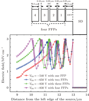
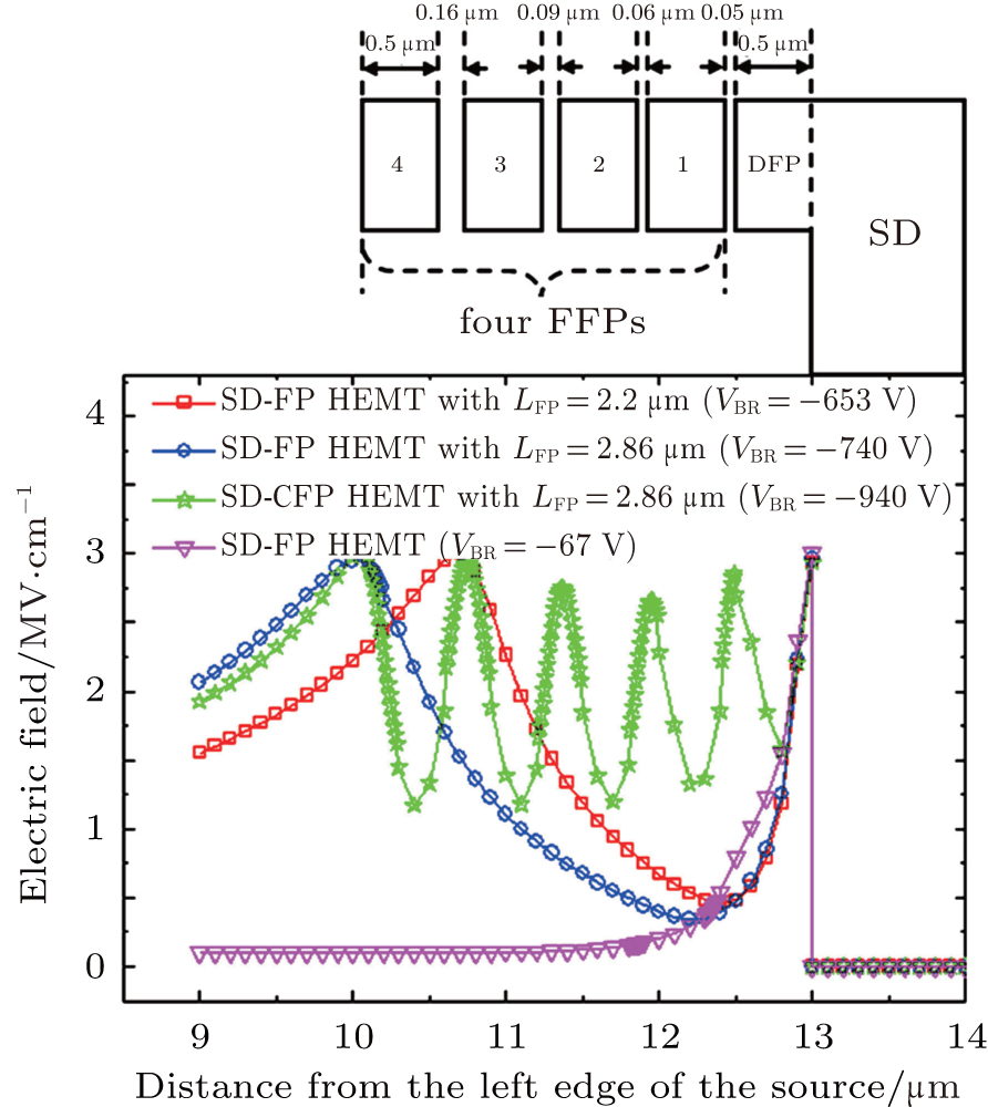
3. Results and discussion Several device parameters, including the SiN passivation thickness d and the spacing s m between two adjacent FFPs, have been optimized in order to make every main channel electric field peak reach 3 MV/cm and obtain the maximum V BR . Figure 2 shows the nearly optimized channel electric field distributions beneath the field plate or around the SD for two conventional SD-FP HEMTs with a DFP of 2.86 μm or 2.2 μm, respectively, an SD-CFP HEMT with four FFPs and L FP = 2.86 μm, and an SD HEMT. The channel electric field distributions away from FP or SD are very small, thus they are not shown in Fig. 2 . In the SD-CFP HEMT, the SD-CFP consists of one DFP and four FFPs, in which both the FFP length and the DFP length are 0.5 μm. As shown in Fig. 2 , the V BR of SD HEMT is only −67 V, with only one electric field peak near the SD edge. It is evident that two nearly equal electric field peaks are formed at the left edge of the drain and the left edge of the DFP in both the SD-FP HEMTs. In the SD-FP HEMT with a 2.2-μm DFP, the optimum d of 0.24 μm is obtained, resulting in a maximum V BR of −653 V, and the V BR will saturate ultimately when the length of the DFP exceeds 2.2 μm with d = 0.24 μm. This is in accordance with our early reports. [ 20 ] With the DFP length L FP increasing to 2.86 μm in the SD-FP HEMT, the passivation layer thickness d is optimized again, and an optimum d of 0.28 μm is obtained, leading to a V BR of −740 V which is a slight increase compared with that of the SD-FP HEMT with a 2.2-μm DFP. In the SD-CFP HEMT, the optimum d is 0.104 μm and the spacing s 1 , s 2 , s 3 , and s 4 , are 0.05 μm, 0.06 μm, 0.09 μm, and 0.16 μm, respectively. As can be seen, four new electric field peaks are formed at the left edge of each FFPs except the two peaks existing in SD-FP HEMT, resulting in a good electric field distribution as high as −940 V. This demonstrates that the CFP with FFPs can effectively offer an increment in reverse breakdown voltage with the same total FP length as the DFP in SD-FP HEMT.
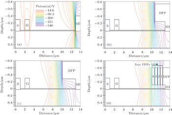
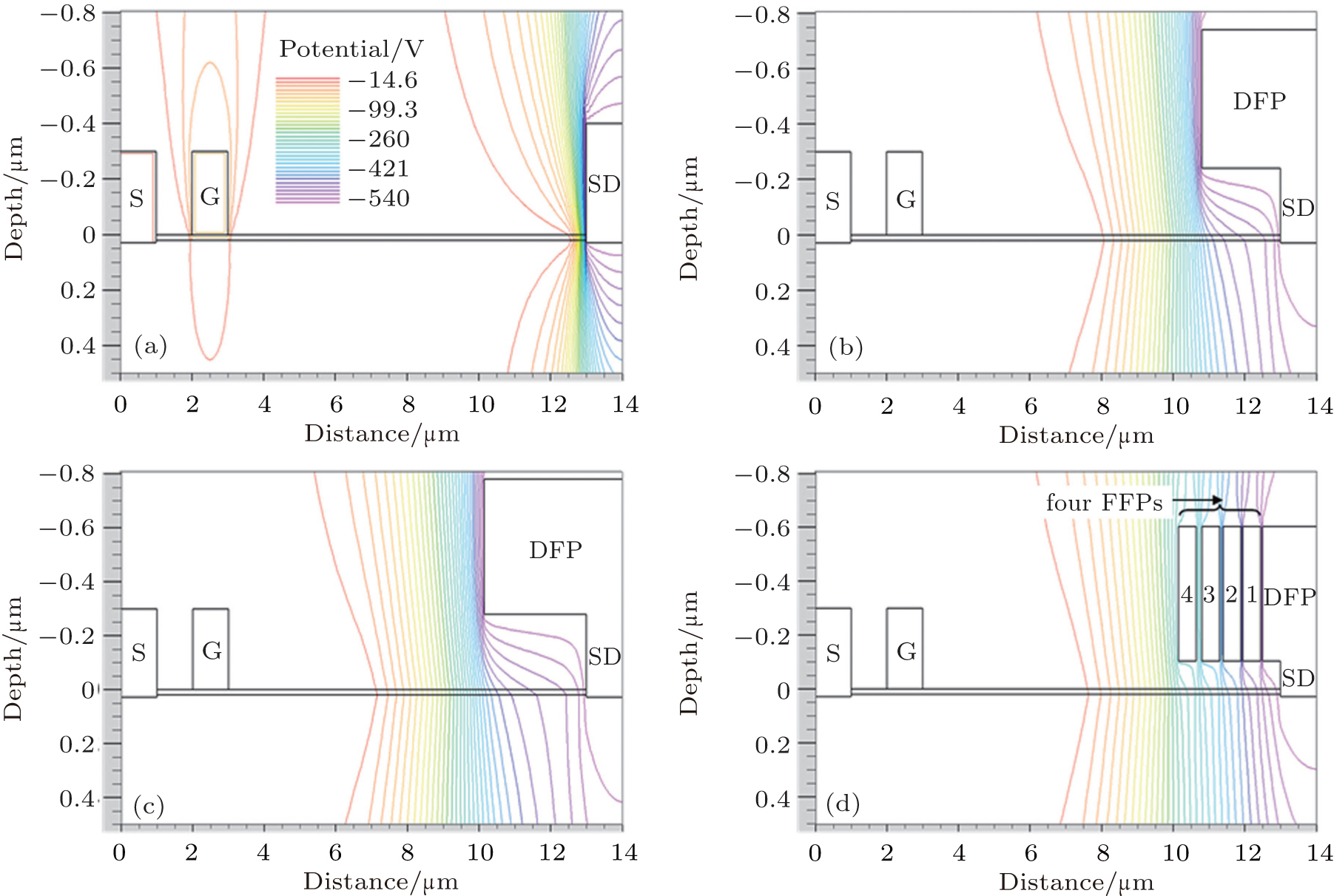
In order to obtain physical insight into the essential mechanism of the modulation of the FFPs, the potential distributions at off-state corresponding to the four devices in Fig. 2 are investigated, as shown in Fig. 3 . In Fig. 3 , it can be observed that most of potential lines crowd around the gate side of the Schottky-drain electrode in SD HEMT, indicating that a high electric field peak could be formed, in accordance with the results in Fig. 2 . For the SD-FP HEMT with an L FP of 2.2 μm or 2.86 μm, the high potential line density appears at two positions, one of which is located at the gate side of the DFP and the other at the gate side of the SD. This is attributed to the modulation effect of the DFP, leading to two electric field peaks in SD-FP HEMTs. Note that, the potential distribution for the 2.2-μm DFP is almost similar to that for the 2.86-μm DFP in the SD-FP HEMT, indicating it is not very effective to improve V BR by increasing the DFP length. For the SD-CFP HEMT with four FFPs, a more uniform distribution of potential lines is observed and six high potential line density areas are formed at the SD edge, DFP edge, and FFPs edge, which shows an excellent and effective modulation of potential lines. Thus, uniform distribution of electric field as well as an outstanding reverse blocking capability could be obtained in SD-CFP HEMT.
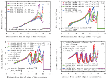
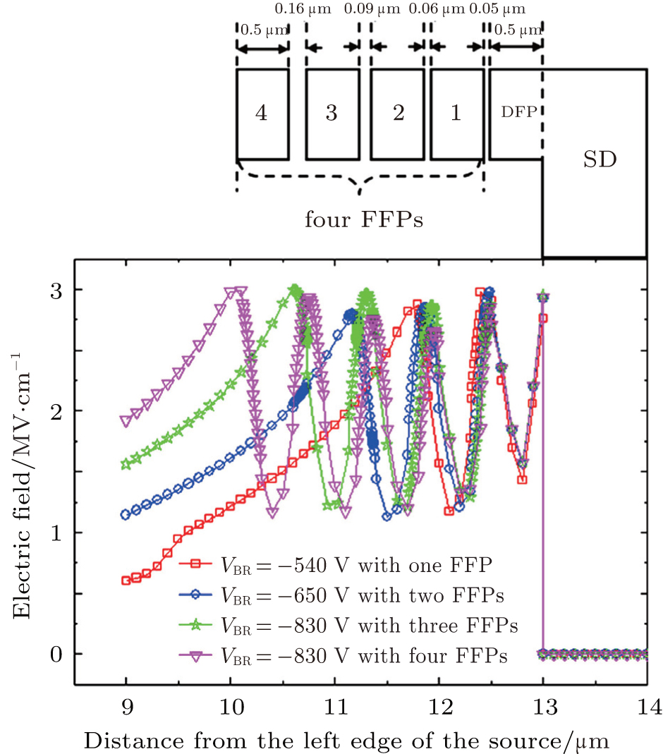
In the SD-CFP HEMTs, there are many parameters needed to be considered during the device optimization. Therefore, the SD-CFP HEMTs with different numbers of FFPs are investigated so as to reveal the optimization procedure. After our systematic studies, two key and useful laws are found. The first law is that the passivation layer thickness d is independent of the number of FFPs, which indicates that the SD-CFP HEMTs with different number of FFPs have the same optimum d as long as all the devices have the same main structure as the DFP and all the FFPs have the same size. Based on this law, if an optimum d is obtained in an SD-CFP HEMTs with one FFP, the d could be used directly as the optimum passivation layer thickness in SD-CFP HEMTs with n FFPs. This could be illustrated in Fig. 4 . As can be seen, the optimized SD-CFP HEMTs with different number of FFPs have the same passivation layer thickness and the number of the approximately equal electric field peaks in device channel rises with an increasing number of FFPs, leading to the enhancement of breakdown voltage V BR . The other law is that the optimum spacing for two adjacent FFPs increases gradually from the DFP to the gate with the characteristics that the optimum spacing s n in the SD-CFP HEMTs with n FFPs is equal to the optimum spacing s n −1 in the SD-CFP HEMTs with n −1 FFPs, as illustrated in Table 2 . Thus, the two laws above are of great value in optimizing device structure and simplifying the actual manufacture processes of SD-CFP HEMTs. Figure 5 shows the detailed optimization procedures of the SD-CFP HEMTs with four FFPs corresponding to Fig. 4 , based on the two laws above. We can see that the passivation layer thickness d of SD-FP HEMT with L DFP = 0.5 μm is optimized by changing the different values of d , first. Then the optimum d of 0.104 μm is obtained and used as the optimum passivation layer thickness in the following optimization of SD-CFP HEMTs with L FFP = L DFP = 0.5 μm. During the optimization of SD-CFP HEMTs with one FFP, the spacing s 1 is optimized and the value of the optimum s 1 = 0.16 μm is obtained and used as the optimum spacing s 2 in SD-CFP HEMTs with two FFPs, namely, s 2 = 0.16 μm. The spacing s 1 of SD-CFP HEMTs with two FFPs is optimized again and s 1 = 0.09 μm and s 2 = 0.16 μm are used as the optimum spacing s 2 and s 3 , respectively, namely s 2 = 0.09 μm and s 3 = 0.16 μm, in SD-CFP HEMTs with three FFPs. Next, the spacing s 1 of SD-CFP HEMTs with three FFPs is optimized once more and the optimum s 1 = 0.06 μm is obtained (not shown for the purpose of concision). The optimum value of s 1 = 0.06 μm, s 2 = 0.09 μm, and s 3 = 0.16 μm are used as the optimum spacing s 2 , s 3 , and s 4 , respectively, namely s 2 = 0.06 μm, s 3 = 0.09 μm, and s 4 = 0.16 μm, in SD-CFP HEMTs with four FFPs. Finally, the spacing s 1 of SD-CFP HEMTs with four FFPs is optimized again and the optimum s 1 = 0.05 μm is obtained. After the optimization, all the optimum spacing s i in SD-CFP HEMTs with different number of FFPs are shown in Table 2 .
Table 2.
Table 2.
Table 2. Characteristics of the optimum spacing s i in the optimized SD-CFP HEMTs with different number of FFPs. L DFP = L FFP = 0.5 μm, d = 0.104 μm in all devices. . | Number of FFPs | s 1 /μm | s 2 /μm | s 3 /μm | s 4 /μm |
|---|
| n = 1 | 0.16 | – | – | – | | n = 2 | 0.09 | 0.16 | – | – | | n = 3 | 0.06 | 0.09 | 0.16 | – | | n = 4 | 0.05 | 0.06 | 0.09 | 0.16 |
| Table 2. Characteristics of the optimum spacing s i in the optimized SD-CFP HEMTs with different number of FFPs. L DFP = L FFP = 0.5 μm, d = 0.104 μm in all devices. . |
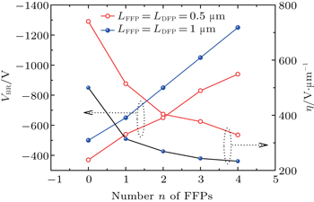
In order to evaluate the ability of SD-CFP to improve the reverse breakdown voltage reasonably, the FP efficiency, [ 16 ] defined as a ratio of the increment of the breakdown voltage to the total FP length L FP is utilized. Figure 6 shows the relationship between the number n of FFPs and the reverse breakdown voltage V BR as well as the FP efficiency η in SD-CFP HEMTs. Two kinds of optimized devices are considered. We set L FFP = L DFP = 0.5 μm and L FFP = L DFP = 1 μm, respectively, in the devices with different number of FFPs. As shown in Fig. 6 , the breakdown voltage and FP efficiency of SD-CFP HEMTs with four FFPs ( L FFP = L DFP = 0.5 μm) and L FP = 2.86 μm are −940 V and 328 V/μm, which are much higher compared to SD-FP HEMT with a 2.2-μm DFP (−653 V and 297 V/μm) and SD-FP HEMT with a 2.86-μm DFP (−740 V and 259 V/μm). As the number of FFPs increases, the reverse breakdown voltage for both kinds of devices increases approximately linearly, which is consistent with the results in Fig. 4 . The breakdown voltage increments (Δ V BR ) per additional FFP are approximately 100 V or 200 V for the devices with L FFP = L DFP = 0.5 μm or L FFP = L DFP = 1 μm, respectively. On the contrary, the FP efficiency decreases approximately linearly with the increasing number of FFPs. For the two kinds of devices with the same number of FFPs, the higher breakdown voltage and the lower FP efficiency could be observed in the devices with longer L FFP and L DFP compared to the devices with shorter L FFP and L DFP . Those results above are helpful for the device designers to optimize the SD-CFP HEMTs and get a proper trade-off between the breakdown voltage and the FP efficiency. In the actual design of SD-CFP HEMTs with a desired breakdown voltage V BR , the L FFP and L DFP are determined by the ability of the photolithography process, which also leads to the available FP efficiency and the available breakdown voltage increment Δ V BR per additional FFP. Therefore, if the breakdown voltage V BR0 of SD-CFP HEMTs with a DFP of L DFP and no FFPs is obtained based on the method in Fig. 5(a) , and set L FFP = L DFP , the number of FFPs could be roughly determined by ( V BR − V BR0 )/Δ V BR . On this basis, the structure of CFP could be determined after the optimization of spacing s i based on the method in Fig. 5 .
It is worth mentioning that the modulation effect of FFPs on the channel electric field mainly depends on the electrostatic induction between two adjacent FFPs as well as between the DFP and the first FFP. The electrostatic induction approximately increases with the couple capacitance C m across two adjacent FFPs, denoted roughly by C m = ε 0 ε ox hw/s m , where ε 0 is the vacuum permittivity, ε ox = 7.5 is the dielectric constant of the SiN passivation layer, s m is the spacing between the No. m FFP and the No. m − 1 FFP, h and w are the thickness and width of FFPs, respectively. Thus, in actual device design, based on the simulation results, one could raise s m by increasing h or w , without changing the value of C m so as to remain the same breakdown voltage. For example, if the width w of FFPs is set to be 10 μm, in the actual device w is usually much larger than 10 μm, the optimum spacings for SD-CFP HEMTs with four FFPs in Table 2 are estimated to be s 1 = 0.5 μm, s 2 =0.6 μm, s 3 = 0.9 μm, and s 4 = 1.6 μm without changing the value of C m , which could significantly reduce the actual device fabrication difficulty. Although the three-dimensional (3D) simulations may be more suitable for study of SD-CFP HEMTs, they may need much more time and suffer more convergence problems. Moreover, the laws in the 3D results are the same as these in our paper.


 , She Wei-Bo 1 , Yang Cui 2 , Zhang Jin-Feng 1 , Zheng Xue-Feng 1 , Wang Chong 1 , Hao Yue 1 ]