Xie Ying-Tao, Ouyang Shi-Hong, Wang Dong-Ping, Zhu Da-Long, Xu Xin, Tan Te, Fong Hon-Hang†. Performance improvement in polymeric thin film transistors using chemically modified both silver bottom contacts and dielectric surfaces. Chinese Physics B, 24(9): 096803
Permissions
Performance improvement in polymeric thin film transistors using chemically modified both silver bottom contacts and dielectric surfaces
Xie Ying-Taoa),b), Ouyang Shi-Honga),b), Wang Dong-Pinga),b), Zhu Da-Longa),b), Xu Xina),b), Tan Tea),b), Fong Hon-Hang†a),b)
Department of Electronic Engineering, Center for Opto–Electronic Materials and Devices, Shanghai Jiao Tong University, Shanghai 200240, China
National Engineering Laboratory for TFT-LCD Key Materials and Technologies, Shanghai 200240, China
*Project supported by the National Basic Research Program of China (Grant No. 2013CB328803).
Abstract
An efficient interface modification is introduced to improve the performance of polymeric thin film transistors. This efficient interface modification is first achieved by 4-fluorothiophenol (4-FTP) self-assembled monolayers (SAM) to chemically treat the silver source–drain (S/D) contacts while the silicon oxide (SiO2) dielectric interface is further primed by either hexamethyldisilazane (HMDS) or octyltrichlorosilane (OTS-C8). Results show that contact resistance is the dominant factor that limits the field effect mobility of the PTDPPTFT4 transistors. With proper surface modification applied to both the dielectric surface and the bottom contacts, the field effect mobilities of the bottom-gate bottom-contact PTDPPTFT4 transistors were significantly improved from 0.15 cm2·V−1·s−1 to 0.91 cm2·V−1·s−1.
Organic thin film transistors (OTFTs) are desired for low-cost electronic devices such as RFID tags and electronic paper.[1– 4] Bottom-contact (BC) transistor geometry is always preferred in the OTFT array layout of the display backplane because the source– drain (S/D) bottom-contact can be scalable by traditional photolithography, which realizes OTFT largescale manufacturing. However, BC OTFTs typically show lower performance due to substantial contact resistance compared with the corresponding top-contact OTFTs.[5– 8]
In order to improve the performance of bottom-contact OTFTs, self-assembled monolayers (SAMs) are widely used to modify the bottom contacts and dielectric interfaces, where functionalized interfaces facilitate better charge injection and transport.[9– 11] On one hand, the SAM treatment of metal contacts allows tuning of the work function so as to match the energy level of the highest occupied molecular orbital (HOMO) of the organic semiconductor (OSC), leading to better ohmic contacts.[12– 15] Moreover, lowering the surface energy of the metal surface is energetically favorable for the alignment of the OSC over the surface of bottom contacts.[16– 21] On the other hand, the SAM treatment of dielectrics helps passivate trap sites at the dielectric surface[22– 24] and enhances the molecular packing of the organic semiconductor along the interface, due to favorable surface assembly.[25– 29]
Modification of bottom contacts and dielectric interfaces can be achieved in different manners. The first approach is to simultaneously modify both bottom-contact Ag electrodes and oxide dielectric surfaces using a single SAM. For example, Acton et al.[30] recently introduced a single n-alkyl phosphonic acid SAM to simultaneously modify both bottom-contact Ag electrodes and hafnium oxide (HfO2) dielectric surfaces so as to achieve desirable properties. However, it is difficult to find out the appropriate SAM material to simultaneously modify the metal and dielectric interfaces. The second approach is to modify the bottom contacts and dielectric interfaces separately using two different SAMs.[13, 14] The problem of this method is chemical compatibility of double SAMs treatment. So far, literature discussing the compatibility of double SAMs treatment on bottom contacts and dielectrics is limited.
In this paper, the compatibility of orthogonal selfassembly to treat bottom contacts and dielectrics independently is evaluated based on a high performance organic semiconductor (PTDPPTFT4) shown in Fig. 1(a), which possesses mobilities > 2 cm2· V− 1· s− 1 for its corresponding top-contact structure.[31] The orthogonal self-assembly means that the first SAM reacts with the bottom contacts while the second SAM interacts only with the dielectric surface. In our bottomcontact OTFT studies, Ag was treated with 4-fluorothiophenol (4-FTP)[32] while the silicon dioxide (SiO2) gate insulator was primed with hexamethyldisilazane (HMDS) or octyltrichlorosilane (OTS-C8). As a result, with 4-FTP and OTS applied to modify the bottom contacts and dielectric surface, the field effect mobilities of the bottom-gate bottom-contact PTDPPTFT4 transistors were significantly improved from 0.15 cm2· V− 1· s− 1 to 0.91 cm2· V− 1· s− 1.
2. Experimental
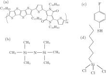
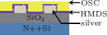
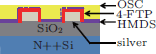
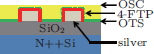
OTFT devices were fabricated using a bottom-contact geometry where Ag is used to form S/D contacts. Heavily doped Si⟨ 100⟩ wafers were used as gate electrodes where a 200-nm thermally grown silicon dioxide layer acts as the gate dielectric layer. The substrates were cleaned by sonication in semiconductor grade acetone and isopropanol, and then given a 2 min. O2 plasma treatment at 20 W under an operating pressure of 0.1 Torr. Silver was thermally evaporated to form the S/D contacts through a metal shadow mask which defines the transistor physical dimension (L = 50– 150 µ m, W = 1000 µ m). Molecule structures of different SAMs are illustrated in Figs. 1(b)– 1(d).
Fig. 1. Molecule structures: (a) organic semiconductor (PTDPPTFT4); (b) 4-fluorothiophenol (4-FTP) used for modification of the silver bottom electrodes; (c) hexamethyldisilazane (HMDS) used for gate oxide modification; (d) octyltrichlorosilane (OTS-C8) used for gate oxide modification.
4-FTP SAM treatment was used to modify the prepatterned Ag bottom electrodes through immersing samples into a 1-mM ethanolic solution of 4-fluorothiophenol (4-FTP from TCI) for 1 h. The 4-FTP-treated Ag electrodes were then removed from the 4-FTP solution and rinsed extensively with anhydrous ethanol and blow dried with N2. The gate oxide was intentionally modified by either HMDS or OTS-C8. In the case of HMDS modification, HMDS was spin coated at a rate of 3000 rpm for 60 s and baked at 120 ° C for 120 s. For the OTS-C8 modification, samples were dipped into a pxylene diluted OTS-C8 solution (1.3 vol%) at room temperature for 60 min, followed by an isopropanol rinse, and then PTDPPTFT4 polymer films were then deposited by spin-coating with the sequence of: 0 RPM for 10 s, 500 RPM for 5 s, 1000 RPM for 60 s, where a 5-mg/mL solution of PTDPPTFT4 in a p-xylene was prepared by stirring at 120 ° C for 20 min. Finally, the samples were annealed in a nitrogen environment at 190 ° C for 60 min. and then cooled to room temperature.
Table 1.
Table 1.
Table 1. Table 1. Devices with different surface modifications.
Device
Component layer
Deposition sequence
A
Ag/OSC
B
Ag/HMDS/OSC
C
Ag/OTS/OSC
D
Ag/4-FTP/OSC
E
Ag/4-FTP/HMDS/OSC
F
Ag/4-FTP/OTS/OSC
Table 1. Table 1. Devices with different surface modifications.
To study the influence of surface modification to bottomcontact OTFT devices, devices with different surface treatments are considered in Table 1. Note that an alternative way of applying two SAM materials to the contacts and dielectric interface is to deposit the first SAM on the entire dielectric surface prior to forming the metal bottom contacts. However, the metal contacts laid down over the SAM treated dielectric can easily peel off due to poor adhesion.
Electrical characteristics of all transistors were measured by a Keithley 4200 SCS in air. All film thicknesses were measured by a KLA-Tencor XP-200 step profiler.
3. Results and discussion
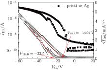
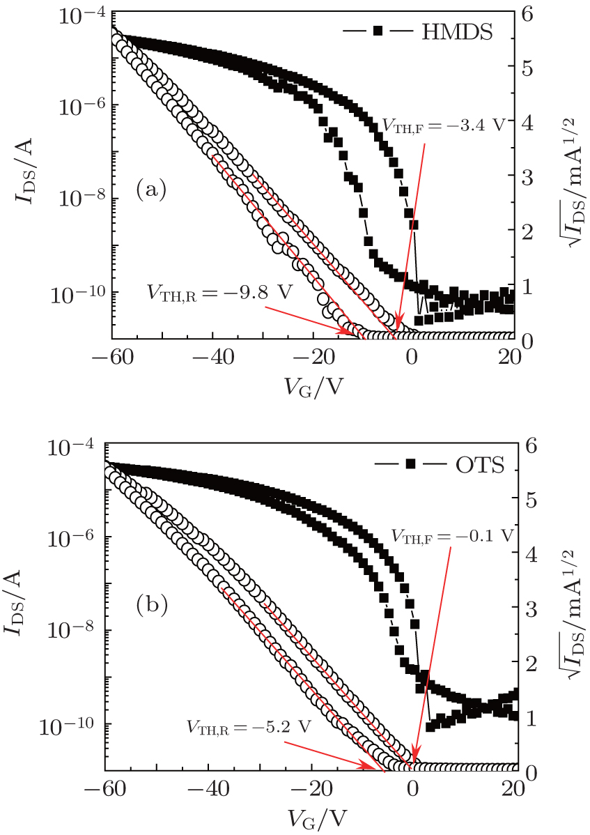
Device A, a control reference, shows lower mobility (0.15 cm2· V− 1· s− 1) and an obvious negative VTH shift (− 14.01 V) (Fig. 2). Under a negative gate-bias stress, the VTH (threshold voltage) in forward and reverse directions is − 14.0 V (VTH, F) and − 22.5 V (VTH, R), respectively. Thus, device A exhibits a negative hysteresis shift (Δ VTH) of − 8.5 V. In order to evaluate the gate oxide surface modification to bottom-contact OTFT devices, HMDS or OTS is used to modify the gate oxide surface. The corresponding transfer curves of device B (HMDS) [Fig. 3(a)] and device C (OTS) [Fig. 3(b)] reveal a slightly negative shift of the VTH to − 3.4 V and − 0.1 V, respectively. In addition, Δ VTH reduces to − 6.4 V and − 5.1 V in devices B and C, respectively. Results suggest that the surface silanol groups of gate oxide passivated by the HMDS or OTS treatment can considerably suppress the VTH shift and device hysteresis. However, these oxide interface treatments do not contribute to the ON current and the device mobility probably due to a significant energy barrier (∼ 0.7 eV) between the HOMO of PTDPPTFT4 (5.3 eV)[30] and the work function of the silver S/D contacts (4.6 eV).
Fig. 3. Transfer characteristics of the devices with the SiO2 gate oxide surface modified with SAMs: (a) HMDS; (b) OTS.
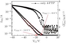
Here, in order to evaluate the metal contact surface modification to bottom-contact OTFT devices, 4-FTP is used to modify the silver bottom-contact surface. The corresponding transfer curve of device D (4-FTP treatment) reveals obvious enhancement in ON current from 10 µ A to 80 µ A and mobility from 0.15 cm2· V− 1· s− 1 to 0.32 cm2· V− 1· s− 1, shown in Fig. 4. The enhancement due to 4-FTP treatment is attributed to better alignment between the HOMO of PTDPPTFT4 (5.3 eV)[30] and the work function of the 4-FTP-treated Ag S/D contact (5.21 eV).[21] This 4-FTP treatment raises the work function of the Ag by 0.51 eV compared to the typical Ag electrode (4.70 eV), [31] resulting in the hole injection barrier lowering.
Fig. 4. Transfer characteristics of the device with Ag S/D contacts modified with 4-FTP and untreated SiO2 dielectrics.
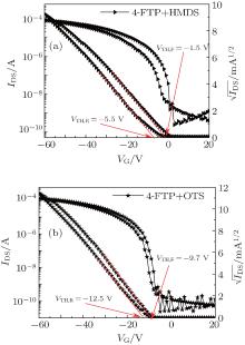
In order to evaluate the device performance through an orthogonal-SAM approach, the samples with 4-FTP treated Ag S/D contacts underwent a second round surface treatment for the gate oxide interface. This surface modification was done by treatment with either HMDS (device E) or OTS-C8 (device F). Figure 5 shows the transfer characteristics of devices E and F.
Fig. 5. Transfer characteristics of the devices with double SAM modification: (a) Ag S/D contacts modified with 4-FTP and SiO2 gate oxides modified with HMDS; (b) Ag S/D contacts modified with 4-FTP and SiO2 gate oxide modified with OTS.
In the double SAM structure adopted in device E, an additional HMDS layer was spin-coated over the substrate where the Ag S/D contacts were as pre-treated with 4-FTP. The corresponding transfer curve of device E [Fig. 5(a)] reveals a slightly positive shift of the VTH to ∼ 0 V that suggests an HMDS modified gate oxide dielectric brings the HOMO of PTDPPTFT4 closer to the energy level of the 4-FTP treated Ag S/D. With this HMDS treatment, the mobility was thus improved substantially from 0.32 (device D) to 0.54 cm2· V− 1· s− 1 (device E). Δ VTH in device E reduces to − 4 V that implies the considerable encapsulation of the surface hydroxyl groups via HMDS priming. Substituting HMDS with OTS-C8 for dielectric surface treatment, device C shows substantially enhanced mobility of 0.91 cm2· V− 1· s− 1 while VTH shows a negative shift to ∼ − 10 V. This negative shift can be understood as being due to the OTS-C8 residue remaining on the contacts. The corresponding Δ VTH further reduces to − 2.8 V while the forward and reserve IV scans are nearly overlapped, showing weak hysteresis. Obviously, OTS-C8 is a more effective SAM in priming the surface hydroxyl groups and leads to an apparent trap-free SiO2 interface.
Table 2 summarizes the average mobility, VTH, oncurrent/ off-current ratio (Ion/off), and contact resistance over five devices. Clearly, in the case of the single SAM treatment, the devices B and C show no enhancement in mobility while theirVTH drift to ∼ 0 V, suggesting both HMDS and OTS treatments help passivating the surface defects of the gate oxide. Device D yields considerable enhancement in mobility, up to 0.24 cm2· V− 1· s− 1, because 4-FTP treatment can improve the work function of silver to better match with the HOMO of OSC. In the case of our double SAM treatment, devices E and F both yield considerable enhancement in mobility, up to 0.44 cm2· V− 1· s− 1 and 0.73 cm2· V− 1· s− 1, while device E shows VTH approaching zero. HMDS is known to be an effective and air-stable primer for terminating the surface hydroxyl groups or dangling bonds. On the contrary, trichlorosilane can react seriously with moisture and leads to self-polymerization such that OTS-C8 is more easily poisoned by the ambient. Therefore, as the second modification layer, the excess amount of OTS-C8 molecules should be completely washed off so as to prevent forming OTS-C8 overlayers over the 4-FTP treated Ag contacts.
Table 2.
Table 2.
Table 2. Electrical properties of PTDPPTFT4 TFTs with various SAM treatments.
No.
Device type
Deposition sequence
Mobility/cm2· V− 1· s− 1
Threshold voltage/V
Ion/off
Contact resistance/kΩ · cm
1
A
Ag/OSC
0.15± 0.13
− 11.01± 2.5
105
200
2
B
Ag/HMDS/OSC
0.15± 0.15
− 3.91± 3.8
107
175
3
C
Ag/OTS/OSC
0.16± 0.17
− 3.76± 5.1
106
154
4
D
Ag/4-FTP/OSC
0.24± 0.04
− 7.2± 2.4
106
45
5
E
Ag/4-FTP/HMDS/OSC
0.44± 0.05
− 0.17± 4.9
105
39
6
F
Ag/4-FTP/OTS/OSC
0.73± 0.16
4.7± 5.8
106
20
Table 2. Electrical properties of PTDPPTFT4 TFTs with various SAM treatments.
For compatibility of double SAMs, we believe that the first chemical modification is achieved through selective chemical reaction of aromatic thiols to the Ag surface. The second modification of either HMDS or silane agents intentionally interacts with the hydroxyl surface of the SiO2 gate insulator. It is more important that thiols tend to react with OH− ions while the dehydrated SiO2 surface only releases H+ ions, which designates our double SAM treatment as an orthogonal assembly. For the reasons for the improved mobility of OTFTs, first chemical modification (4-FTP treatment Ag surface) can raise the work function of the Ag by 0.51 eV compared to the typical Ag electrode (4.70 eV), and then modification of the SiO2 surface with OTS-C8 or HMDS can generally passivate trap sites at the dielectric surface (e.g., − OH groups[22] or dielectric ionic polarization[23, 24]) and improve the packing of the OSC through SAM/OSC physical interaction. Due to compatibility of double SAMs, these orthogonal double SAMs can greatly improve the performance of OTFT compared to single SAMs or an untreated Ag electrode. As a result, the maximum mobility of the OTFT devices obtained with orthogonal self-assembly of 4-FTP and OTS was 0.91 cm2· V− 1· s− 1.
The charge injection behavior of bottom contacts can be quantified by its parasitic resistance Rp (or namely contact resistance), which is calculated by the transition line method.[33] The extracted contact resistances were calculated for devices A– F according to
where Ron is device resistance during on state, Rch is channel resistance, and Rp is contact resistance. From Table 2, with only the SiO2 insulating layer modified by either HMDS or OTS-C8 (devices B and C), the bottom Ag devices show slightly lower Rp (154– 175 kΩ · cm) compared to the bottom Ag device (device A), indicating that both HMDS and OTS-C8 slightly deviate Rp. OTS is likely to lift up the vacuum level due to its interface dipole and thus assists hole injection, yet the hole injection barriers in devices B and C are considerably larger even compared to the bottom 4-FTP treatment Ag contact device.
With 4-FTP treatment over Ag S/D contacts, device D shows a reduction of RpW from 200 kΩ · cm to 45 kΩ · cm over the untreated reference device (device A). Similar observations (devices E and F) also illustrate that 4-FTP-modified Ag contacts bring RpW down to 39 kΩ · cm and 20 kΩ · cm when the SiO2 dielectric surface is further primed with HMDS or OTS-C8, respectively. RpW of double-SAM treated devices (devices E and F) is < 1/4 of the single gate oxide treated devices (devices B and C). This comparison clearly indicates that 4-FTP treatment consistently suppresses the RpW of Ag S/D contacts to one quarter of the original and leads to high mobility PTDPPTFT4 transistors.
4. Conclusion
A compatible and efficient interface modification using an orthogonal-SAM approach was achieved by first modification of silver bottom contacts with 4-FTP, followed by a second modification of the SiO2 gate dielectric interface with OTS-C8 or HMDS. The optimized performances from 4-FTP + OTS-C8 treated PTDPPTFT4 transistors were determined to exhibit an average mobility of 0.73± 0.16 cm2· V− 1· s− 1, and a highest mobility of 0.91 cm2· V− 1· s− 1. This demonstrates that an orthogonal self-assembly approach is effective for enhancing the overall performance of bottom-contact OTFTs. Results also show that contact resistance is the dominant factor that limits the field effect mobility of the PTDPPTFT4 transistors.
GelinckG H, HuitemaH E A, VeenendaalE V, CantatoreE, SchrijnemakersL, Vand erPuttenJ B P H, GeunsT C T, Been-hakkersM, GiesbersJ B, HuismanB H, MeijerE J, BenitoE M, TouwslagerF J, MarsmanA W, van RensJ E B and de LeeuwD M2004Nat. Mater. 3106DOI:10.1038/nmat1061[Cited within:1]
3
SunQ J, XuZ, ZhaoS L, ZhangF J, GaoL Y, TianX Y and WangY S2010Acta Phys. Sin. 598125(in Chinese)[Cited within:1]
4
ZouJ H, LanL F, XuR X, YangW and PengJ B2010Acta Phys. Sin. 591275(in Chinese)[Cited within:1]
5
SteudelS, MynyK, ScholsS, ViccaP, SmoutS, TripathiA, van der PuttenB, van der SteenJ L, van NeerM, SchützeF, HildO R, van VeenendaalE, van LieshoutP, van MilM, GenoeJ, GelinckG and HeremansP2012Org. Electron. 131729DOI:10.1016/j.orgel.2012.05.034[Cited within:1]
6
IshikawaY, WadaY and ToyabeT2010J. Appl. Phys. 107053709DOI:10.1063/1.3309935[Cited within:1]
SmitsE C P, MathijssenS G J, van HalP A, SetayeshS, GeunsT C, MutsaersK A H A, CantatoreE, WondergemH J, WerzerO, ReselR, KemerinkM, KirchmeyerS, MuzafarovA M, PonomarenkoS A, de BoerB, BlomP W M and de LeeuwD M2008Nature455956DOI:10.1038/nature07320[Cited within:1]
ActonO, DubeyM, WeidnerT, MalleyK M O, KimT W, TingG G, HutchinsD, BaioJ E, LovejoyT C, GageA H, CastnerD G, MaH and JenA K Y2011Adv. Funct. Mater. 211476DOI:10.1002/adfm.v21.8[Cited within:3]
31
MatthewsJ R, NiuW, Tand iaA, WallaceA, HuJ, LeeW Y, GiriG, MannsfeldS C B, XieY, CaiS, FongH H, BaoZ and HeM2013Chem. Mater. 25782DOI:10.1021/cm303953e[Cited within:2]
32
HongJ P, ParkA Y, LeeS, KangJShinN and YoonD Y2008Appl. Phys. Lett. 92143311DOI:10.1063/1.2907691[Cited within:1]
33
GundlachD J, ZhouL, NicholsJ A, JacksonT N, NecliudovP V and ShurM S2006J. Appl. Phys. 100024509DOI:10.1063/1.2215132[Cited within:1]
1
2011
0.0
0.0
... [1#cod#x2013 ...
1
2004
0.0
0.0
1
2010
0.0
0.0
1
2010
0.0
0.0
... 4] Bottom-contact (BC) transistor geometry is always preferred in the OTFT array layout of the display backplane because the source#cod#x2013 ...
1
2012
0.0
0.0
... [5#cod#x2013 ...
1
2010
0.0
0.0
1
2003
0.0
0.0
1
2002
0.0
0.0
... 8] ...
1
2010
0.0
0.0
... [9#cod#x2013 ...
1
2009
0.0
0.0
1
2008
0.0
0.0
... 11] On one hand, the SAM treatment of metal contacts allows tuning of the work function so as to match the energy level of the highest occupied molecular orbital (HOMO) of the organic semiconductor (OSC), leading to better ohmic contacts ...
1
2006
0.0
0.0
... [12#cod#x2013 ...
1
2009
0.0
0.0
... [13,14] The problem of this method is chemical compatibility of double SAMs treatment ...
1
2001
0.0
0.0
... [13,14] The problem of this method is chemical compatibility of double SAMs treatment ...
1
2005
0.0
0.0
... 15] Moreover, lowering the surface energy of the metal surface is energetically favorable for the alignment of the OSC over the surface of bottom contacts ...
1
2008
0.0
0.0
... [16#cod#x2013 ...
1
2001
0.0
0.0
1
2006
0.0
0.0
1
2007
0.0
0.0
1
2005
0.0
0.0
2
2009
0.0
0.0
... 21] On the other hand, the SAM treatment of dielectrics helps passivate trap sites at the dielectric surface[22#cod#x2013 ...
... [21] This 4-FTP treatment raises the work function of the Ag by 0 ...
2
2005
0.0
0.0
... 21] On the other hand, the SAM treatment of dielectrics helps passivate trap sites at the dielectric surface[22#cod#x2013 ...
... OH groups[22] or dielectric ionic polarization[23,24]) and improve the packing of the OSC through SAM/OSC physical interaction ...
1
2006
0.0
0.0
... OH groups[22] or dielectric ionic polarization[23,24]) and improve the packing of the OSC through SAM/OSC physical interaction ...
2
2010
0.0
0.0
... 24] and enhances the molecular packing of the organic semiconductor along the interface, due to favorable surface assembly ...
... OH groups[22] or dielectric ionic polarization[23,24]) and improve the packing of the OSC through SAM/OSC physical interaction ...
1
2004
0.0
0.0
... [25#cod#x2013 ...
1
2009
0.0
0.0
1
2008
0.0
0.0
1
2006
0.0
0.0
1
2009
0.0
0.0
... 29] ...
3
2011
0.0
0.0
... [30] recently introduced a single n-alkyl phosphonic acid SAM to simultaneously modify both bottom-contact Ag electrodes and hafnium oxide (HfO2) dielectric surfaces so as to achieve desirable properties ...
... eV)[30] and the work function of the silver S/D contacts (4 ...
... eV)[30] and the work function of the 4-FTP-treated Ag S/D contact (5 ...
2
2013
0.0
0.0
... [31] The orthogonal self-assembly means that the first SAM reacts with the bottom contacts while the second SAM interacts only with the dielectric surface ...
... eV),[31] resulting in the hole injection barrier lowering ...
1
2008
0.0
0.0
... In our bottomcontact OTFT studies, Ag was treated with 4-fluorothiophenol (4-FTP)[32] while the silicon dioxide (SiO2) gate insulator was primed with hexamethyldisilazane (HMDS) or octyltrichlorosilane (OTS-C8) ...
1
2006
0.0
0.0
... [33] The extracted contact resistances were calculated for devices A#cod#x2013 ...
Performance improvement in polymeric thin film transistors using chemically modified both silver bottom contacts and dielectric surfaces
[Xie Ying-Taoa),b), Ouyang Shi-Honga),b), Wang Dong-Pinga),b), Zhu Da-Longa),b), Xu Xina),b), Tan Tea),b), Fong Hon-Hang†a),b)]


 ]
]