


Charge trapping behavior and its origin in Al2O3/SiC MIS system
[Liu Xin-Yua) , Wang Yi-Yua) , Peng Zhao-Yanga) , Li Cheng-Zhanb) , Wu Jiab) , Bai Yuna) , Tang Yi-Dana) , Liu Ke-Anb) , Shen Hua-Jun†a)  ]
]
]
|
|


†Corresponding author. E-mail: shenhuajun@ime.ac.cn
*Project supported by the National Natural Science Foundation of China (Grant No. 61106080) and the National Science and Technology Major Project of the Ministry of Science and Technology of China (Grant No. 2013ZX02305).
Charge trapping behavior and its origin in Al2O3/SiC MOS structure are investigated by analyzing the capacitance–voltage ( C– V) hysteresis and the chemical composition of the interface. The C– V hysteresis is measured as a function of oxide thickness series for an Al2O3/SiC MIS capacitor. The distribution of the trapped charges, extracted from the C– V curves, is found to mainly follow a sheet charge model rather than a bulk charge model. Therefore, the electron injection phenomenon is evaluated by using linear fitting. It is found that most of the trapped charges are not distributed exactly at the interface but are located in the bulk of the Al2O3 layers, especially close to the border. Furthermore, there is no detectable oxide interface layer in the x-ray photoelectron spectroscope (XPS) and transmission electron microscope (TEM) measurements. In addition, Rutherford back scattering (RBS) analysis shows that the width of the Al2O3/SiC interface is less than 1 nm. It could be concluded that the charge trapping sites in Al2O3/SiC structure might mainly originate from the border traps in Al2O3 film rather than the interface traps in the interfacial transition layer.
The SiC metal-oxide semiconductor field-effect transistor (MOSFET) is a promising power transistor for high efficiency application. However, there are still many problems stemming from its gate dielectric (SiO2), which is generated by thermal oxidation, such as low channel mobility and low reliability.[1– 10] Alternative gate insulators have aroused increasing interest, especially in high permittivity (high-k) dielectrics, due to their ability to reduce both the electric field and the leakage current across the gate insulator. Among various high-k dielectrics, aluminum oxide (Al2O3) is a possible candidate due to its high dielectric constant (7– 9), wide band gap (6.2 eV– 7.0 eV), and high conduction band offset (1.7 eV) on 4H– SiC.[11– 15]
Al2O3 film grown by atomic layer deposition (ALD) has demonstrated its excellent potential to be applied to SiC MOSFETs, which was proven to have ultra-high carrier mobility and low interface-trap density.[16– 18] However, Al2O3 films have the microstructures and chemical natures different from those of SiC substrates. Therefore, the electrical properties of Al2O3/SiC structure grown by ALD method are not as good as expected due to the high density of charge trapping sites existing at the interface or in the bulk oxide.[19] These charge trapping sites can be manifested as hysteresis in the C– V response, resulting in device instability. Some studies demonstrate that the C– V hysteresis of Al2O3/SiC structure could be reduced by high-temperature annealing, whereas the amorphous Al2O3 layer begins to crystallize and a sub-oxide layer forms at the interface after being annealed at 900 ° C in an inert gas atmosphere.[15, 20, 21] In addition, forming gas annealing (FGA) has also been used to improve the interfacial properties Al2O3/substrate.[22] The hydrogen in the FGA is useful to passivate the dangling bonds, whereas it seems to have no distinct effect on the reduction of the C– V hysteresis.[23] Furthermore, an ultrathin SiO2 layer has been inserted between the Al2O3 and SiC substrate as a barrier layer against electron injection.[24, 25] Significant VFB shifts are still observed under a high electric field and the properties of Al2O3/SiO2/SiC structure appear to be dominated by the SiO2/SiC interface, exhibiting a high Dit close to Ec.[19, 26– 28] So far, the issue of C– V hysteresis in Al2O3/SiC MOS system has not been solved. The density, physical position, and origin of the charge trapping sites are still not clear. The study of C– V hysteresis is important because it provides a method to analyze and quantify the density and physical distribution of charge trapping sites. Thus, a better understanding of the origin of the charge trapping sites can be gained and further improvements can be achieved based on these experimental results.
In this work, we investigate the charge trapping behavior and its origin by analyzing the C– V hysteresis and the chemical composition of Al2O3/SiC interface. To examine the density and distribution of the trapped charges, C– V hysteresis is measured as a function of oxide thickness series for Al2O3/SiC MIS capacitor. It is found that the distribution of the trapped charges mainly follows a sheet charge model and the actual distribution of the trapped charge is not applicable for the case at the interface. Furthermore, the microstructures of the interface are investigated by XPS, TEM, and RBS measurements. No distinct interface oxide is found through XPS measurement or TEM measurement, indicating that an abrupt interface is achieved. It can therefore be concluded that the charge trapping sites in Al2O3/SiC structure originate from the native defects in Al2O3 film, predominantly the border traps. These experimental results also provide an insight into methods that can further reduce the density of trapping sites.
N-type, 4° off (0001) oriented, 4H– SiC wafers with 12-μ m thick epilayer (ND ∼ 8× 1015 cm− 3) of nitrogen were used. The thickness and resistivity of each of the n-type SiC substrates were 350 μ m and 0.023 Ω · cm, respectively. These wafers were purchased from the EpiWorld International Co. Ltd. The wafers were cleaned by the conventional Radio Corporation of America (RCA) clean procedure, and then dipped into a diluted hydrofluoric acid solution to remove native oxide from the SiC surface. Al2O3 films of different thickness values, 12.9 nm– 50 nm, were deposited by ALD technique at 350 ° C using TMA and water as precursors. MIS capacitors were fabricated to evaluate the electrical characterization. The gate pads were patterned into circles each with a diameter of 100 μ m. Then 20 nm/200 nm Ni/Au layers were deposited by e-beam evaporation and followed by lift-off process. A 200-nm Al layer was sputtered to form the back contact. For x-ray photoelectron spectroscopy (XPS) analysis, a thin Al2O3 film (2 nm) on a 4H– SiC substrate was prepared. In addition, a 21.6-nm Al2O3 film on the 4H– SiC substrate was prepared for TEM and RBS measurements.
Film thickness was determined by UVISEL spectroscopic ellipsometry and TEM. The ellipsometry model was adjusted according to TEM results. The triple-angle method with incident angles of 65° , 70° , and 75° was applied to optical properties and thickness of the Al2O3 film. The C– V measurements were conducted by the Agilent 4284A precision impedance analyzer at room temperature (1 kHz∼ 1 MHz) under dark condition. All the C– V hysteresis measurements were performed in voltage steps of 0.1 V. The sweep voltages were measured by starting from inversion, and sweeping towards the accumulation region, and subsequently sweeping back towards inversion. There was no hold time in accumulation. The interface state density (Dit) was determined by the conductance technique. The capacitance and conductance were measured in a frequency range from 1 kHz to 1 MHz. Before applying the conductance method, the values of the series resistance were determined for each frequency from the impedance measured in a strong accumulation region. Then, series resistance was removed from the measured capacitance and conductance.[29] The interface state density is linked to GP by
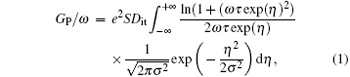
where GP is the interface state conductance, ω is the angular frequency, S is the area of the gate electrode, and e (1.602× 10 − 19 C) is the elementary electric charge. The interface state density (Dit), the time constant of the interface states (τ ), and the standard deviation (σ ) are determined using a simple method provided by Nicollian and Brews.[29] The energy level (Ec– ET) of interface states is calculated from

by taking into account the Fermi level of the SiC epilayer (Ec-0.21 eV) at room temperature. Here Ψ s is the surface potential determined from a comparison of ideal C– V curve and measured high frequency C– V curve.[29] XPS analysis was performed by using a Thermo SCIENTIFIC ESCALAB 250 spectrometer equipped with a monochromatic Al Kα x-ray source (1486.6 eV) from a 90° take-off angle (normal to surface). The atomic structures at the interface and in the bulk Al2O3 were investigated through the peak deconvolution of Si 2p and Al 2p photoelectron spectra. The microstructure and the composition of the Al2O3/SiC interface were investigated by TEM and RBS.
To examine the density and distribution of the trapped charges, the C– V hysteresis is measured as a function of oxide thickness series for Al2O3/SiC MIS capacitors. Both the bulk charge model and the sheet charge model are used to fit the curves of C– V hysteresis versus physical thickness (tox).[30] For the bulk charge model, the trapped charges are considered to be uniformly distributed throughout the oxide. The C– V hysteresis is then proportional to the square of the oxide thickness, as expressed below

where ε 0 is the vacuum permittivity, ε k is the relative permittivity of Al2O3, tox is the physical thickness, and Qtrapped is the population of trapped charge in cm − 2. For the sheet charge model, the trapped charges are located at the interface or in a plane within the oxide. The C– V hysteresis increases linearly with the increasing of oxide thickness. This linear relationship can be expressed by the following equation:

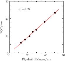
During the C– V measurements, keeping the same maximum electric field (Emax) in the accumulation region (i.e., the same Emax = (Vmax− VFB)/tox) is very important for Al2O3/SiC MIS capacitors with varying oxide thickness values. The comparison is valid because the same quantity of majority carriers will accumulate at the SiC surface when the values of Emax are the same. Figure 1 presents the relationship between the equivalent oxide thickness (EOT) and physical thickness (tox) for Al2O3/SiC MOS structures with tox ranging from 12.9 nm to 50 nm. The EOT is calculated from the capacitance in accumulation region of 1-kHz C– V curve. The dielectric constant of Al2O3 extracted from the slope of the EOT versus tox curve is 8.39. VFB is extracted from the maximum capacitance in accumulation (Cmax) and the minimum capacitance in depletion (Cmin) from 1-MHz C– V curves. The dielectric capacitance (Cox) is extracted from the capacitance and conductance measured in strong accumulation region. The Cmin coupled with Cox is used to determine the substrate capacitance in depletion, allowing an evaluation of the substrate doping level. The total capacitance in the flat band condition is then calculated from the substrate capacitance in the flat band condition and Cox. The substrate doping concentrations have also been obtained from the reciprocal of the slope of the 1/C2 versus
 | Fig. 1. Plot of the EOT versus tox for MIS capacitors with tox ranging from 12.9 nm∼ 50 nm. |
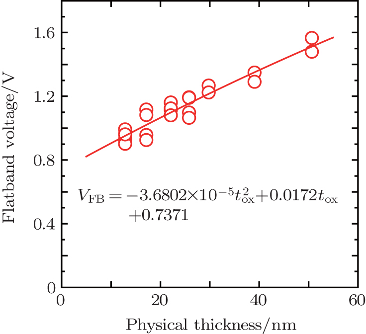 | Fig. 2. Plot of VFB versus tox for Al2O3/SiC MIS capacitors. |
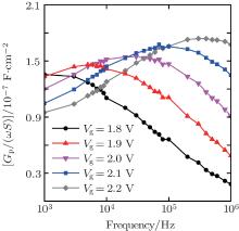
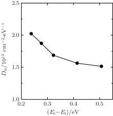
VG curves.[31] For both methods, the calculated substrate doping concentrations are both about 8× 1015 cm − 3, which is consistent with the data offered by the wafer producer. The extracted VFB as a function of oxide thickness is depicted in Fig. 2. The Dit is extracted from the Gp/ω -frequency characteristics by the conductance technique, as shown in Fig. 3. Figure 4 shows the Dit as a function of the position in the band-gap from a 12.9-nm Al2O3/SiC sample.
 | Fig. 3. Curves of Gp/(ω S) versus frequency at several biases for a 12.9-nm Al2O3/SiC MIS capacitor. S is the area of the capacitor. |
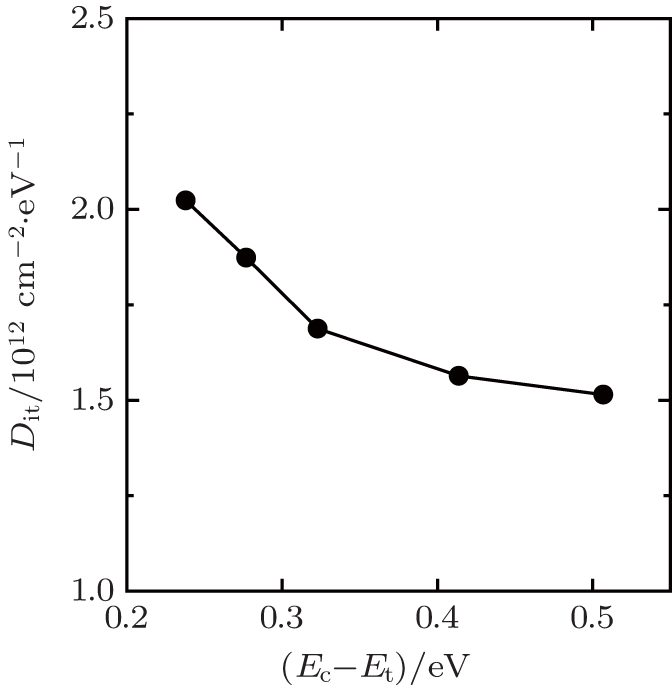 | Fig. 4. Plot of the density of interface states as a function of the position in the band gap, calculated from GP/(ω S) versus frequency data from Fig. 3. |
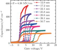
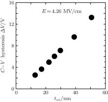
The C– V hysteresis (1 MHz) is measured as a function of oxide thickness series for Al2O3/SiC MIS capacitors at different maximum electric fields (3.10, 3.49, 3.87, and 4.26 MV/cm). The change of the VFB as a function of oxide thickness is also taken into consideration to determine the Emax. For example, in order to achieve a maximum electric field of 4.26 MV/cm for all the samples, the maximum voltages in the accumulation region are varied from 6.5 V to 23.5 V for Al2O3 layers with different thickness values, as shown in Fig. 5. The C– V hysteresis is estimated from the shift of VFB between forward and backward C– V curves. Both quadratic fit and linear fit have been adopted to fit the C– V hysteresis versus tox curves, which are summarized in Table 1. For the quadratic fitting, the quadratic coefficients are all kept at a value of 0.0016, indicating that the densities of the injected electrons in the bulk Al2O3 films are kept constant under different values of Emax. However, the linear coefficients increase rapidly with the increase of the Emax. It can be concluded that the majority of the charge trapping possibly occurs in a plane near the Al2O3/SiC interface and is not uniformly distributed throughout the oxide. Thus, a simple sheet charge model approximation (linear fit) is used to evaluate the actual effect of the electron injection phenomenon, as depicted in Fig. 6. The Qtrapped is extracted from the slope of linear fit, based on Eq. (4). The injected charge quantity increases with increasing the value of Emax and reaches a highest value, i.e., 1.29× 1013 cm − 2, at an Emax of 4.26 MV/cm, as shown in Table 1. When the Al2O3/SiC capacitor is biased at a high electric field, the trap levels in Al2O3 layer, which are primarily located above the SiC conduction band under the flat band condition, will be located below the SiC conduction band.[32] Then, the electron trapping from the substrate is energetically favorable. As the maximum electric field increases, more charge trapping sites will be located below the SiC conduction band and the extent of SiC band bending will also be aggravated. Thus, more electrons will be injected into the Al2O3 layer from SiC substrate. The level of trapped charge sites is comparable to the interface states density (Dit) of Al2O3/SiC structure (2.02× 1012 cm − 2· eV − 1 at Ec– Et= 0.23 eV), which highlights the importance of electron trapping in Al2O3/SiC system. Furthermore, it can be noted that none of the linear fitted lines intersect the origins of the plot and the intercepts of X axis are all on the right half axis in Table 1. If the electrons are injected into the interface of Al2O3/SiC, then the fitted line should follow the format of Eq. (4) and pass through the origin of the plot. We speculate that most of the trapped charges are not distributed exactly at the interface but are located in the bulk of the Al2O3 layers and they are especially close to the border, resulting in the right shift of fitted line along the X axis. A similar behavior has been reported in Si-based MOS capacitors with Al2O3/SiO2 gate stacks.[28, 33] So the equivalent injection depths of the trapped charges can be extracted from the intercept of X axis from the linear fitting formulas. For the Emax values ranging from 3.10 MV/cm to 4.26 MV/cm, the equivalent injection depths, extracted from the intercepts of X axis, are 3.53, 3.19, 3.29, and 3.69 nm, respectively.
 | Fig. 5. Bi-direction C– V curves for MIS capacitors with an Emax value of 4.26 MV/cm (gate swings from − 5 V to Vmax and then back to − 5 V). |
 | Fig. 6. C– V hysteresis as a function of oxide thickness for Al2O3/SiC MIS capacitors. |
| Table 1. Fitting formulas of C– V hysteresis versus tox curves. Both the Qtrapped and the equivalent injection depths are extracted from the linear fitting formulas. |
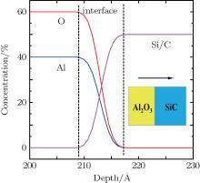
The microstructure and chemical structure of the Al2O3/SiC interface are also investigated to further seek the origin of these charge trapping sites. As shown in Fig. 7, no distinct interface transition layer is found between the amorphous Al2O3 layer and 4H– SiC substrate through the TEM measurement. The plots of composition of the Al2O3/SiC film versus the depth are shown in Fig. 8, which is calculated from the RBS data. The width of the Al2O3/SiC interface (the transition from SiC layer into Al2O3 layer) is limited to less than 1 nm. Considering the fact that the injection depth is a distance ranging from 3 nm to 4 nm, the distribution of the trapped charges is far from the interface. To analyze the XPS data, the spin– orbit splitting of Al 2p spectra is considered from Al 2p3/2 and Al 2p1/2 lines split by 0.41 eV and an intensity ratio of 2:1. Figure 9(a) shows the Al 2p spectra of 2-nm Al2O3/SiC sample. The XPS curves can be well fitted by two Gauss peaks corresponding to the Al2O3. It is indicated that Al2O3 is formed at the first 2 nm. But, this does not mean that defects relating to Al do not exist in the film. Considering that the density of the charge trapping sites is about 1× 1013 cm − 2 and the Al areal density in Al2O3 layer is 6.94× 1016 cm − 2, it is beyond the measurement range of XPS method. The Si 2p spectra are deconvoluted into two components corresponding to the Si atoms from the bulk SiC substrate and the Si atoms in the intermediate oxide states (Si 1+ ), as shown in Fig. 9(b). As reported by Gao et al., the Si1 + atomics form a monolayer on top of SiC and below Al2O3, right at the interface.[13] So in the ALD process, the Al2O3 layer is attached by bridging oxygen atoms to the topmost Si layer of 4H– SiC (0001) surface. This oxygen bridge has also been reported at Al2O3/Si interface.[34, 35] It is commonly believed that the presence of Al2O3 has been concluded in catalyzing the oxidation of Si (SiC). The intermediate oxide
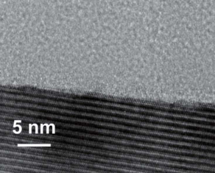 | Fig. 7. TEM image, showing the interface region of a 21.6-nm Al2O3 film on the 4H– SiC substrate. |
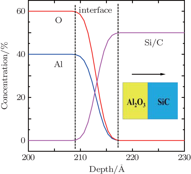 | Fig. 8. Variations of composition of the Al2O3/SiC films with depth. |
states 1+ of silicon atoms originate from Si– O– Al bond at the interface between Al2O3 and SiC. No other sub-oxides of Si are found and it may benefit from the reported “ self-cleaning” effect of the ALD Al2O3 process.[36] A sharp interface is achieved, which accords with our TEM result.
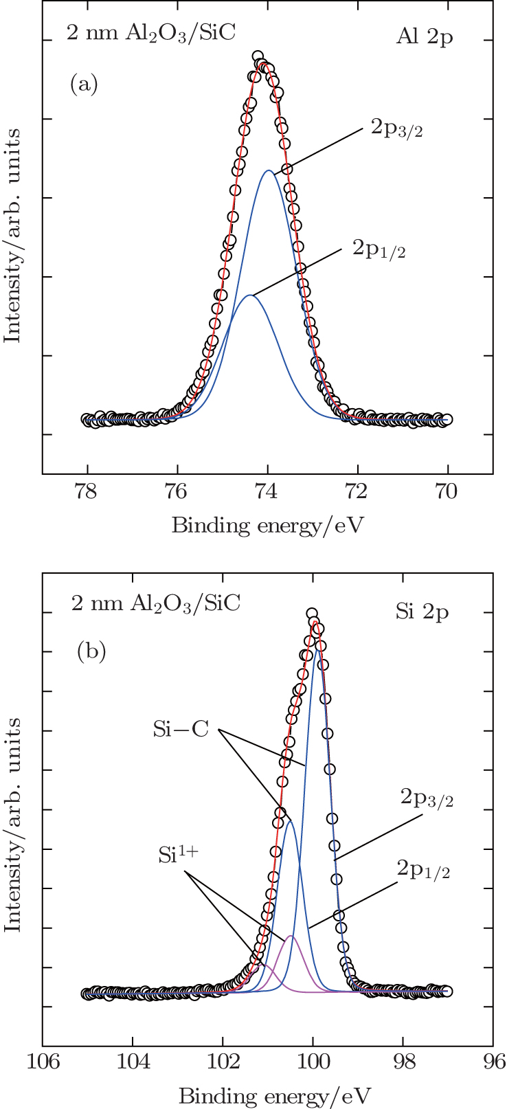 | Fig. 9. XPS spectra of (a) Al 2p in 2-nm Al2O3 on 4H– SiC substrate, and (b) Si 2p in 2-nm Al2O3 on 4H– SiC substrate. |
Charge trapping behavior in an Al2O3/SiC MOS structure is investigated. C– V hysteresis is measured as a function of oxide thickness series for Al2O3/SiC MIS capacitors. The distribution of the trapped charges mainly follows a sheet charge model rather than a bulk charge model. Then, a linear fitting is adopted to evaluate the density and injected depth of the trapped charges. A remarkable C– V hysteresis is observed and the density of trapped charges could be as high as 1013 cm − 2. The injection depths are 3.53, 3.19, 3.29, and 3.69 nm for the Emax values ranging from 3.10 MV/cm to 4.26 MV/cm. It is revealed that the actual distribution of the trapped charges is not applicable for the case at the interface. No distinct interface transition layer is found in the TEM result or in the XPS result. The intermediate oxide states 1+ of silicon atoms in XPS results are attributed to Si– O– Al bond at the interface of Al2O3 and SiC. According to the RBS data, the width of transition from SiC to Al2O3 is less than 1 nm. These results indicate that a sharp interface is achieved between Al2O3 and SiC. It can be concluded that charge trapping sites in Al2O3/SiC structure originate from the native defects in Al2O3 film rather than the interface traps in the interface transition layer. Further research into the improvement of quality of Al2O3 film is still required to reduce the number of charge trapping sites.
| 1 |
|
| 2 |
|
| 3 |
|
| 4 |
|
| 5 |
|
| 6 |
|
| 7 |
|
| 8 |
|
| 9 |
|
| 10 |
|
| 11 |
|
| 12 |
|
| 13 |
|
| 14 |
|
| 15 |
|
| 16 |
|
| 17 |
|
| 18 |
|
| 19 |
|
| 20 |
|
| 21 |
|
| 22 |
|
| 23 |
|
| 24 |
|
| 25 |
|
| 26 |
|
| 27 |
|
| 28 |
|
| 29 |
|
| 30 |
|
| 31 |
|
| 32 |
|
| 33 |
|
| 34 |
|
| 35 |
|
| 36 |
|