2. Model and methodThe schematic structure of the OFeFET to be simulated is presented in the inset of Fig. 1. It shows a top-gate and top-contact configuration with P3HT as the active layer, P(VDF-TrFE) as the ferroelectric layer, and Al as the gate, source, and drain electrodes. First we will give some brief introductions on those theories correlative with our simulation work. Note that here we directly quote the final equations from those related references without any derivation.
2.1. Ferroelectric polarizationElectrical polarization P depends on the electric field applied to the ferroelectric film and its previous history. Though it is still an open question how to find a physical model for the description of polarization hysteresis, a numerical and empirical model is widely accepted for this purpose. In this model, the polarization is described as a function of the electric field applied to the ferroelectric film (Eferro). The first polarization of an unpolarized ferroelectric film is defined by[9– 11]
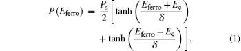
with

where Ps is the spontaneous polarization of the ferroelectric film. The resulting polarization depends on the maximum applied field Emax. Then, to obtain a complete polarization– electrical field (P– E) hysteresis loop, the polarization as a function of the electrical field below Emax is given as
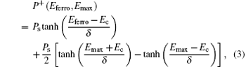
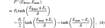
where P+ and P− signify the positive- and the negative-going branches of the P– E loop. Here we set Ps = 0.08 C/m2, Pr = 0.07 C/m2, and Ec = 50 MV/m, which are representative for electrical properties in ferroelectric P(VDF-TrFE) films.[15, 16]
2.2. Polarization fatigueExperimentally, the polarization fatigue in ferroelectric polymer films is characterized by the decrease of Pr. Usually Pr degradation can be empirically fitted to the stretched exponential[15, 16]

where Pr0 of 0.07 C/m2 is the remanent polarization before the fatigue process, while PrN is the remanent polarization after N fatigue cycles, β is a stretching factor, f is the frequency of the applied fatigue field, and τ is a characteristic decay time. Such stretched exponentials, known as the William– Watts decay, are invoked in a wide variety of physical phenomena.[17] Thus the spontaneous polarization after the N-th fatigue cycle (PsN) can be approximately estimated by

Here we assume that during the fatigue process, the decrease in the spontaneous polarization is equal to the decrease in the remanent polarization.
Typical values of β = 0.32, f = 1.0 kHz, and τ = 5.1 × 10⁵ s are obtained from our previous work[15] and are used here to evaluate the influence of the ferroelectric fatigue on the electrical characteristics of OFeFETs.
2.3. Ferroelectric switching transientThe ferroelectric switching transient in ferroelectric polymer films is well experimentally studied and can be approximately expressed as a function of time t[8, 18]

where D is the electrical displacement, ε o is the permittivity of a vacuum, ε = 12 is the relative permittivity of the ferroelectric layer, ts is the switching time, γ is a parameter related to the shape of the switching curve, and σ is the dc conductivity. We consider an ideal ferroelectric film with σ = 0. Dielectric capacitance Cferro of the ferroelectric layer can be approximately evaluated by Cferro = ε oε S/d, where S is the electrode area and d = 500 nm is the film thickness. We can obtain the dielectric capacitance of the ferroelectric layer, which is about 2.1 × 10− 4 C/m2, much smaller than the ferroelectric polarization of Ps = 0.08 C/m2. So here we only consider the contribution of the ferroelectric polarization and neglect the influence of the dielectric capacitance. A large number of experimental observations indicate that the switching time ts is Eferro-dependent and can be described by the exponential law

where ts∞ is a limited switching time of 5 ns, and Ea is an activation field of 1 GV/m, [8] which are consistent with the experimental measurements obtained for a 1.0 μ m thick P(VDF-TrFE) film.[19] Both values will be further validated by experimental measurements of ferroelectric switching transient below, and γ will be determined by fitting the ferroelectric switching curves with Eq. (7).
2.4. Charge transport in OFeFETsThe charge transport in inorganic field-effect transistors has been well and quantitatively described.[9] However, it is hard to be directly used for organic semiconductors, because the charge carrier mobility in organic semiconductors is dependent on the carrier density.[12] Recently, a standard model has been developed for the simulation of organic field-effect transistors (OFETs), which is based on variable range hopping of charge carriers in an exponential density of localized states with parameters directly linked to the physical properties of the semiconductor such as the width of the density of states. The charge transport in a unipolar organic transistor is expressed as a function of the applied gate bias and the operation temperature[12– 14]
with
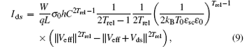
where ε o is the permittivity of a vacuum, kB is the Boltzmann constant, Vds is the voltage applied to the drain electrode, W and L are the channel width and length, σ 0 is a conductivity prefactor, α − 1 is an effective overlap parameter, BC is related to the onset of percolation and given by 2.8 for three-dimensional systems, [20]Trel = T0/T with T0 being a characteristic temperature describing the width of the density of states, C is the gate capacitance per unit area, ε sc is the dielectric constant of the semiconductor, and q is the elementary charge. The Vso is the switch-on voltage, defined as the gate voltage at which there is no band bending in the semiconductor. For OFeFETs, the effective gate bias Veff can be written as

and Eferro can be written as a function of the gate voltage Vg and the thickness of the ferroelectric layer (dferro)

Note that, as for this model, it is assumed that the potential in the active channel is uniform between source and drain. To meet this assumption, we define a narrow channel geometry with W/L = 1 mm/10 μ m and a thicker ferroelectric film of 500 nm so that small Vds of several volts and large Vg as high as 100 V can be applied. The other parameters are set according to the fitting results for P3HT-based OFeFETs[12, 21] and listed below: σ 0 = 2.86 × 10⁶ S/m, T0 = 350 K, T = 300 K, α − 1 = 2.6 Å , Vso = 2 V, and the dielectric constant of the ferroelectric P(VDF-TrFE) is 12.
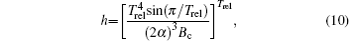
3. Results and discussionThe OFeFET structure used for our calculation is shown in the inset of Fig. 1. P(VDF-TrFE) and P3HT are used as ferroelectric and semiconducting layers, respectively. The source is electrically grounded, and gate Vg and drain Vds voltages are applied to the gate and the drain, respectively.
First we consider the polarization– Vg (P– Vg) hysteresis loop of the ferroelectric layer and the polarization-modulated transfer characteristic of an OFeFET at various gate voltages. Typical results are shown in Fig. 1, where the gate voltage is varied from 50 V to 100 V. The P– Vg loops show anticlockwise hystereses (Fig. 1(a)), consistent with the experimental observations of ferroelectric P(VDF-TrFE) films. As for the transfer characteristic shown in Fig. 1(b), the ferroelectric polarization modulates the charge transport of the active channel, resulting in a clockwise hysteresis (memory window). To emphasize the modulation of the ferroelectric polarization on the electrical performance of OFeFETs, we also calculate the output characteristic of a standard OFET with a 500 nm thick SiO2 layer instead of the ferroelectric P(VDF-TrFE) layer. The relative dielectric constant of the SiO2 layer is set to 3.9. The output curve of this OFET structure is also shown in Fig. 1(b). Obviously, for this standard OFET structure without ferroelectric modulation, the transfer curve shows no hysteresis. Furthermore, the drain current in the OFeFET structure at a negative gate voltage is more than one order of magnitude larger than that in the OFET structure, which can be attributed to the modulation of the ferroelectric polarization. Note that, in our calculations, an ideal semiconducting layer is assumed, which can be completely switched off without any current leakage, resulting in zero drain current at the off state.
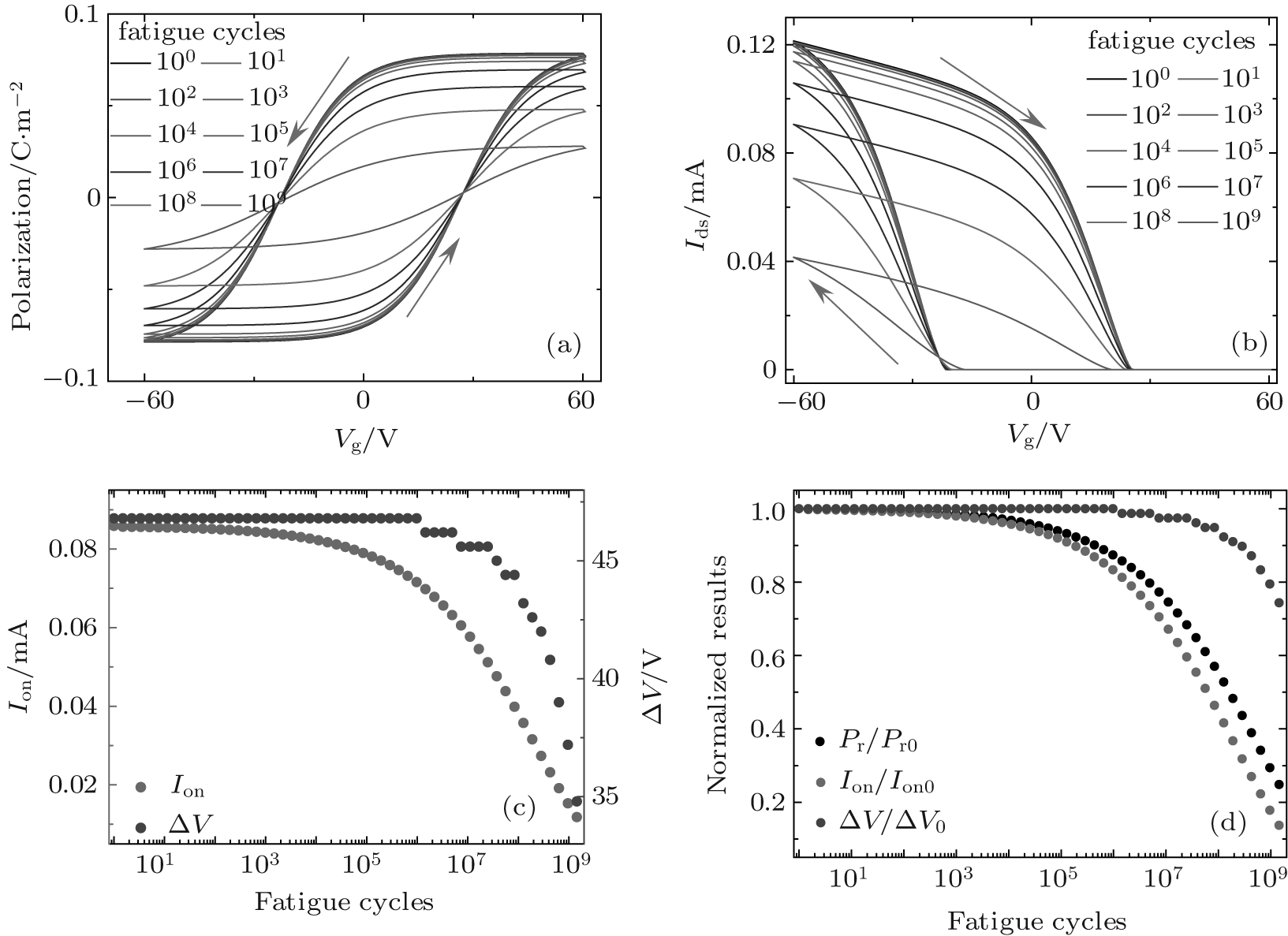
We now consider the polarization-fatigue-induced degradation of transfer characteristic in the OFeFET device. The Pr and Ps during the fatigue process are approximately estimated according to the empirical Eqs. (5) and (6) and then the P– Vg hysteresis loops and the transfer curves are obtained using Eqs. (3), (4), and (10). Typical results are shown in Fig. 2, where a fatigue gate voltage with amplitude of 60 V and frequency of 1.0 kHz is applied. Figure 2(a) shows the change in P– Vg loops with fatigue cycles and indicates nearly the same trend as that experimentally observed in P(VDF-TrFE) films: gradually rounded hysteresis loop and decreased polarization. The corresponding transfer curves are shown in Fig. 2(b). In our calculation, the obtained off-state drain current is always zero during the fatigue process, while the on-state drain current gradually decreases with fatigue cycles. Furthermore, the width of the memory window gradually decreases during the fatigue process. We calculate the maximum width of the memory window, Δ V, to quantitate the change in the width of the memory window with fatigue cycles. From Fig. 2(b), Δ V occurs at zero drain current. Figure 2(c) shows the decrease of the on-state drain current Ion at Vg = 0 V and the maximum window width Δ V with fatigue cycles, while figure 2(d) shows the normalized degradation of Ion, Δ V, and Pr. Obviously, Ion degrades much faster than Δ V. In our calculation, Δ V keeps a constant of 46.8 V at an early fatigue state with less than 106 fatigue cycles and then decreases with the further increase of fatigue cycles. This indicates that, at the early fatigue state, though the remanent polarization decreases to 87.4% of its initial value, the polarization in the ferroelectric layer is still high enough to keep switch-on and switch-off voltages constant and thus maintain Δ V. From Fig. 2(d), we can see that window width Δ V decreases the most slowly, while Ion shows the fastest degradation, which may result in fast decrease of the on/off ratio.
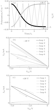
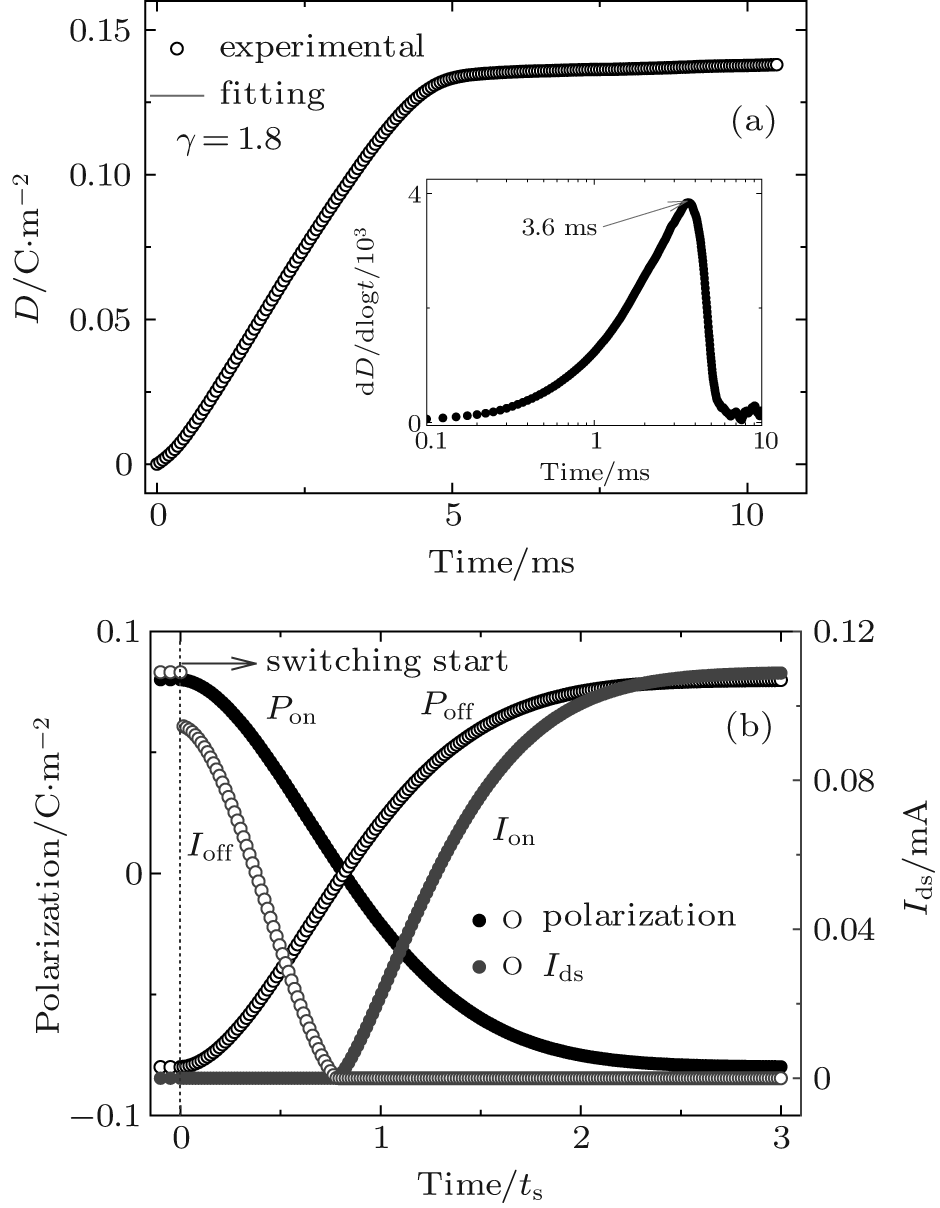
Next, we consider the influence of the ferroelectric switching transient on the electrical characterization in OFeFETs. To determine the γ value and further validate both ts∞ and Ea in Eq. (7), first we prepare an Al/P(VDF-TrFE)/Al sandwich structure for the experimental measurement of the ferroelectric switching transient. Ferroelectric films are prepared by spin-coating technique from a 5.0% by weight solution of 60/40 P(VDF-TrFE) in butanone onto Al deposited glass substrates. The films are annealed at 140 ° C for 4 h to increase their crystallinity. Then the Al top electrodes are vacuum deposited. The ferroelectric films have a thickness of about 518 nm, as measured by an atomic force microscope (Nanoscope V, Veeco Inc., USA). Note that, though 518 nm thick 60/40 P(VDF-TrFE) thin films are used here to determine the ferroelectric switching transient, the simulation results are suitable for other P(VDF-TrFE) films with various thicknesses and various VDF/TrFE molar ratios.
Switching time ts can be determined by time domain measurements of the charge response induced by a stepwise electric field.[8] The relations between the electric displacement, the applied field, and the switching time can be well described by Eq. (7). In the electrical measurements, the bottom electrode is always grounded and the applied voltage is applied to the top electrode. First, a pulse of − 40 V is applied for 1.0 s to remove the previous polarization history and then the film was re-polarized by a pulse of + 40 V, resulting in dipole reorientation. The resulting current response is recorded and integrated with respect to the time to determine the time dependence of the electrical displacement D. Typical D– t characteristic is shown in Fig. 3(a). By fitting the D– t curve in Fig. 3(a) with Eq. (7), a representative γ value of 1.8 is determined. The switching time of 3.6 ms is further obtained from the time of the maximum dD/d log t shown in inset of Fig. 3(a).
According to Eq. (8) with ts∞ = 5 ns and Ea = 1 GV/m, we obtain a nominal switching time of 2.1 ms for the 518 nm thick film polarized by a voltage of 40 V, well consistent with the experimental value of 3.6 ms. Both ts∞ and Ea values of 5 ns and 1 GV/m, respectively, are suitable for our calculations.
Based on Eqs. (7) and (9), we can further evaluate what happens to drain current measurements during ferroelectric switching transients. Figure 3(b) shows the time dependence of the polarization reversal and thus the induced change in the drain current. Polarization switching starts at 0ts; before 0ts ferroelectric polarization is pre-set at stable positive or negative polarization states, and therefore the OFeFET device stays at completely switch-off or switch-on state.
When a negative writing pulse is applied, the ferroelectric layer is switched from positive (P = 0.08 C/m2) to negative (P = − 0.08 C/m2) polarization state, and the OFeFET device tends to be switched on. However, at the very beginning of the application of the writing pulse, the ferroelectric polarization still stays at its pre-set positive polarization state, thus resulting in switch-off of the OFeFET device and zero drain current. The drain current Ids at Vds = − 3 V keeps being 0 mA (off-state) in the early 0.78ts, corresponding to a polarization of 0.0044 C/m2. With the further increase of switching time, the polarization gradually reverses from positive to negative, which is helpful to enhance the drain current. The OFeFET device is switched on and Ids gradually increases to the maximum on-state current of 0.11 mA in the rest time of 3ts.
As a comparison, when a positive erasing pulse is applied, the OFeFET device tends to be switched off. However, at the very beginning of the pulse application, the polarization stays at its pre-set negative polarization state, which enhances the drain current and thus results in the largest drain current of 0.11 mA. Once the erasing pulse is applied, the drain current sharply decreases and then, with the increase of time, the negative polarization gradually decreases and thus weakens its enhancement effect on the drain current. The Ids decreases from 0.11 mA to 0 mA in the early 0.78ts, corresponding to a polarization of − 0.0044 C/m2, and then keeps being 0 mA in the rest time of 3ts. At 0.78ts, the negative polarization is too low to keep the switch-on of the OFeFET device, thus resulting in zero drain current and the complete switch-off of the OFeFET device. Longer time can be helpful for complete polarization reversal but do no good to the drain current.
Here we can see the critical influence of the pulse duration on the efficient switches between on- and off-states in OFeFETs.
1) If the OFeFET is switched from on- to off-state by a positive erasing pulse, a pulse duration of 0.78ts is long enough to realize a complete switch-off of the active channel, though at this time the polarization only changes from − 0.08 C/m2 to − 0.0044 C/m2.
2) If the OFeFET is switched from off- to on-state by a negative writing pulse, a pulse duration of 0.78ts is the lower limit to start the switch-on of the OFeFET device and to make sure a large enough negative polarization for the maximum drain current; an even longer pulse duration, for example 2.5ts, is required for complete switch-on.
3) From Eqs. (9) and (11) and also from our calculated results in Fig. 3, we know that the larger the negative polarization, the larger the drain current. With the same pulse amplitude, it is suggested that for the OFeFET operation, the on-state writing pulse duration (for example, ∼ 2.5ts) should be much longer than the off-state erasing pulse duration (for example, ∼ 0.78ts).
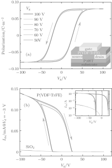
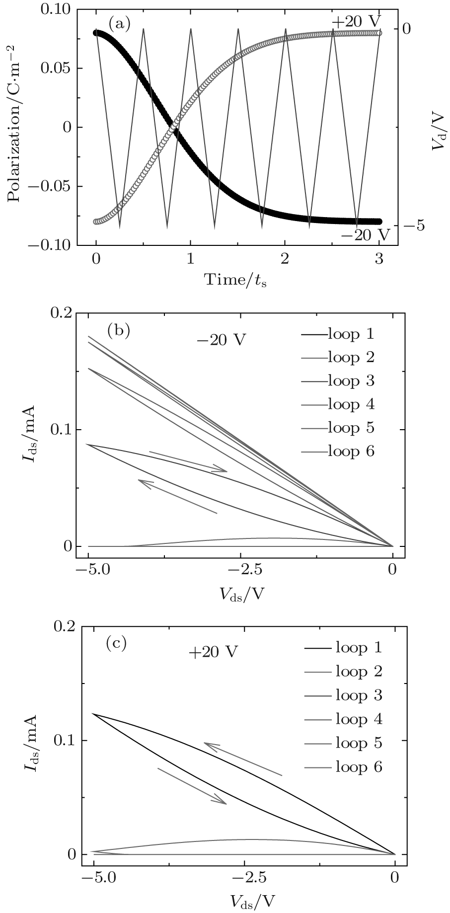
Furthermore we hope to determine what happens if the output characteristic is measured during the ferroelectric switching process. First, we consider the situation that the semiconducting layer is switched from off- to on-state. The ferroelectric layer is positively pre-polarized and then re-polarized by a low gate voltage of − 20 V, which results in a much longer switching time ts of 37 s so that several output loops can be experimentally measured in a time range of 3ts. Polarization in the ferroelectric layer is slowly switched from positive to negative polarization state by − 20 V gate voltage and simultaneously six consecutive triangular Vds pulses scanning between 0 and − 5 V are applied in a time range of 3ts as shown in Fig. 4(a). The corresponding six output loops are shown in Fig. 4(b). At the early stage of ferroelectric switching, the change in polarization is not enough to switch on the active channel, so no drain current can be observed (loop 1). As time increases, more dipoles are reversed, resulting in the switch-on of the channel, observable Ids is obtained but the calculated output loops show clockwise hystereses (loops 2– 4) due to the continuous change in polarization from positive to negative state resulting in gradually enhanced polarization modulation of the drain current. Finally, the polarization is completely reversed and a large drain current is observed but the output loops show no hysteresis (loops 5 and 6).
Second, the semiconducting layer is switched from on- to off-state and the drain current is recorded during ferroelectric switching. The ferroelectric layer is negatively pre-polarized and then re-polarized by a gate voltage of + 20 V and simultaneously six consecutive triangular Vds pulses scanning between 0 and − 5 V are applied in a time range of 3ts. The polarization reversal with the time is shown by the red curve in Fig. 4(a), while the corresponding six output loops are shown in Fig. 4(c). At the early state of ferroelectric switching, the OFeFET device is not switched off, we still obtain an observable drain current (loops 1 and 2); however, due to the polarization switching from negative to positive polarization state, which tends to turn off the drain current, the obtained output curves (loops 1 and 2) show anticlockwise hystereses, opposite to those loops obtained when the OFeFET device is switched from off- to on-state (Fig. 4(b)). After 0.78ts (∼ 1.56 loops), the semiconducting channel is completely switched off by a large enough positive polarization, resulting in zero drain current (loops 3– 6).
From these calculations, we can see that the dynamic switching process in the ferroelectric layer can also result in clockwise or anticlockwise hystereses in the output measurements. In the experimental measurements of OFeFETs, to obtain stable and repeatable output characteristics, it is necessary to make sure that the measurements are performed under stable polarization state.
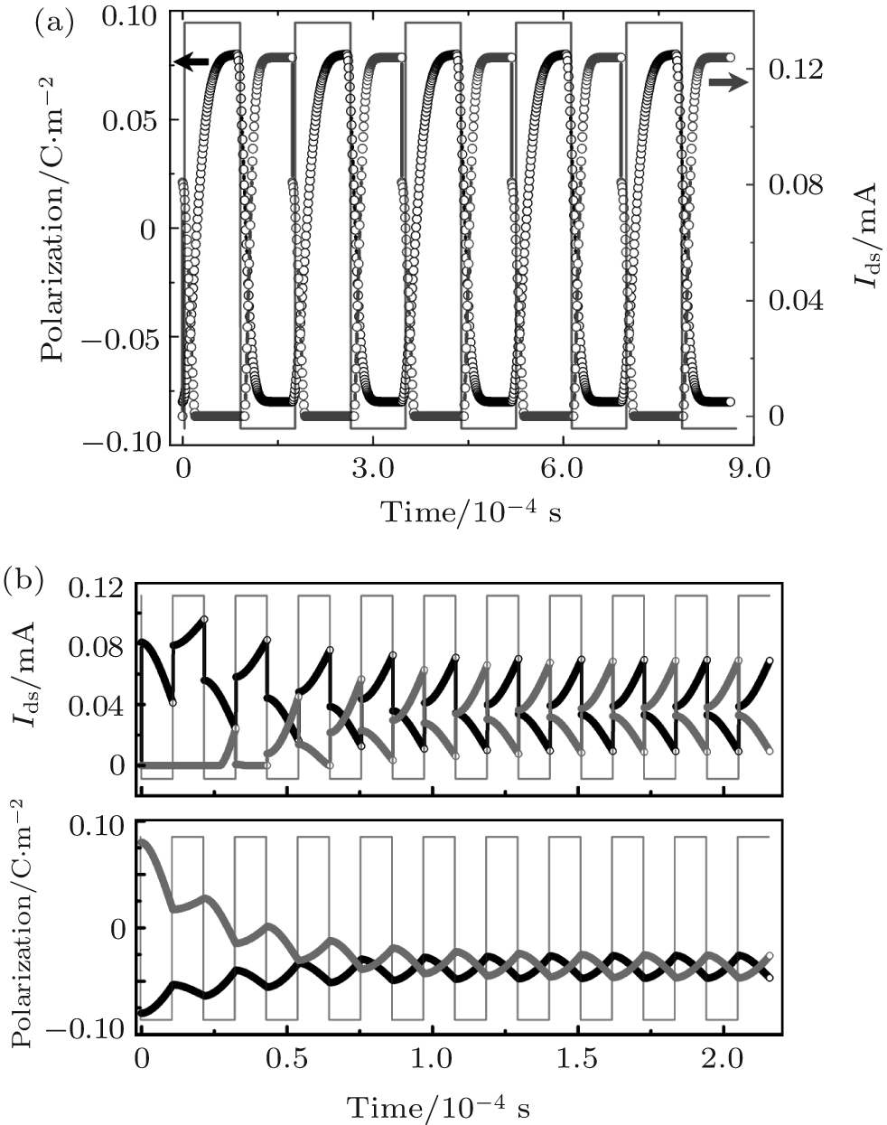
In experimental measurements of field-effect transistor memories, researchers usually prefer to apply continuous writing/erasing (W/E) pulses to switch on/off the active channel in order to illuminate the separation of on- and off-states and the ability for repeated writing and erasing. However, here we want to demonstrate that the frequency (or period) of the W/E pulses will greatly influence the observed results, especially the separation of on- and off-states. For this purpose, bipolar rectangular W/E gate pulses with 50% duty ratio, 60 V amplitude, and various frequencies are applied. Note that, according to Eqs. (8) and (12), the writing and the erasing pulses result in different Eferro (− 124 MV/m and + 116 MV/m, respectively) due to non-zero Vso (here Vso = 2 V) and thus different switching time of ts_ON = 15.9 μ s and ts_OFF = 27.7 μ s, where ts_OFF indicates the switching time as the polarization is switched from negative to positive polarization state by the positive erasing gate voltage, while ts_ON indicates the switching time as the polarization is switched from positive to negative polarization state by the negative writing gate voltage.
Figure 5(a) shows the calculated results for repeated polarization switches and sequent on/off drain current in an OFeFET as a function of time when five bipolar rectangular pulses are applied with a period of 4 × (ts_OFF + ts_ON), equivalent to a W/E frequency of 5.7 kHz. In this case, the pulse period is long enough to ensure the complete switch between positive and negative polarization states, so the semiconducting channel can be completely switched on and off. This is the ideal situation which shows no influence of the W/E gate pulse period on the on/off measurements.
However, with the further decrease of the W/E pulse period (or the increase of the pulse frequency), a pulse-period-dependent on/off characteristic is gradually observed. Typical results are shown in Fig. 5(b), where ten bipolar W/E pulses are applied with a period of (ts_OFF + ts_ON)/2, equivalent to a frequency of 45.6 kHz. During the application of W/E pulses, the ferroelectric layer suffers asymmetric ferroelectric reversal due to different Eferro of − 124 MV/m and + 116 MV/m for writing and erasing pulses, respectively. The duration of one writing (erasing) pulse is (ts_OFF + ts_ON)/4 = 10.9 μ s, corresponding to 0.39ts_OFF and 0.68ts_ON. This duration is too short for both writing and erasing pulses to completely reverse the polarization. Furthermore, according to the ferroelectric switching results shown in Fig. 3(b), in every W/E cycle, the negative writing gate pulse of 0.68ts_ON can cause more polarization reversal than the positive erasing pulse of 0.39ts_OFF. Therefore, after several W/E cycles, the ferroelectric polarization tends to be negatively polarized, no matter whether the ferroelectric layer is pre-polarized to a negative or positive polarization state, as can be seen in Fig. 5(b). In the figure, the black curves correspond to the results when the ferroelectric layer is assumed to be initially in a negative polarization state and then the positive erasing and the negative writing (E/W) pulses are sequentially applied, while the red curves are the results when the ferroelectric layer is initially in a positive polarization state and then the negative writing and the positive erasing (W/E) pulses are sequentially applied.
First we consider the results shown by the black curves, where the data are obtained from an OFeFET with a negatively pre-polarized ferroelectric layer. Here we define PON and Ids_ON as the final polarization and the final drain current measured when negative writing pulses of the E/W gate pulses are applied, and POFF and Ids_OFF as the final polarization and the final drain current measured when positive erasing pulses are applied. Though the polarization is modulated by the bipolar E/W pulses, both PON and POFF gradually degrade in the first five E/W pulses, and then stay nearly constant in the rest of the five periods. Compared with the polarization modulation Δ P (Δ P = | PON – POFF| ) of 0.16 C/m2 in Fig. 5(a), a small polarization modulation of only 0.021 C/m2 is observed in Fig. 5(b). The corresponding polarization-modulated Ids_ON and Ids_OFF also gradually reach to their stable values after five W/E pulses. Note that the final off-state drain current Ids_OFF is ∼ 9.4 μ A due to the incomplete switch-off of the active channel and the final on-state drain current Ids_ON of 68.7 μ A is much smaller than Ids_ON of 124 μ A in Fig. 5(a). Furthermore, we observe the oscillatory degradation of polarization and Ids especially at the early several E/W cycles, which have the same period as that of the applied W/E pulses. This oscillation is due to the alternate application of positive erasing and negative writing pulses which cause positive and negative polarization reversals, respectively, and the gradual degradation is due to the asymmetric ferroelectric reversal induced by different writing and erasing fields.
As for the red curves obtained from an OFeFET with a positively pre-polarized ferroelectric layer, the polarization also shows oscillatory degradation from the initial + 0.08 C/m2 to negative values and, after five W/E pulses, both PON and POFF gradually reach to their stable values resulting in stable Δ P of 0.021 C/m2. The polarization-modulated drain current gradually increases and Ids_ON and Ids_OFF finally reach at their stable values of 68.9 μ A and 9.38 μ A, respectively.
Note that, whether the ferroelectric layer in OFeFETs is negatively or positively pre-polarized, the same W/E pulses will finally result in the same modulation of polarization and thus the same on/off drain currents.
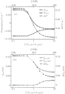
The quantitative changes in PON, POFF, and Δ P as a function of W/E pulse frequency f and f × (ts_OFF+ ts_ON) are shown in Fig. 6(a), while the consequent changes in Ids_ON, Ids_OFF, and Δ Ids are shown in Fig. 6(b), where Δ Ids is defined as Δ Ids = | Ids_ON – Ids_OFF| . Obviously, for a W/E frequency lower than 7.6 kHz (or  ), PON and POFF show no observable changes and are independent of the W/E frequency, so the corresponding Ids_ON and Ids_OFF are also independent of the W/E frequency and show the maximum separation (or the maximum on/off ratio); while, with the increase of the W/E pulse frequency, PON and POFF degrade until Δ P is hardly distinguished, for example, Δ P is only about 0.0011 C/m2 at the frequency of 228 kHz (or
  ). As a comparison, Δ P is as large as 0.16 C/m2 at a frequency below 7.6 kHz. However, though PON and POFF begin to degrade at frequency larger than 7.6 kHz, Ids_ON and Ids_OFF show degradation at frequencies of 11.4 kHz (or
  ) and 22.8 kHz (or
  ), respectively. To some extent, the degradation of the on/off drain currents lags behind that of polarization. In our calculations, the separation Δ Ids of the on- and off-state drain currents decreases from 124 μ A at lower frequency to 35 μ A at the frequency of 228 kHz.
From all these results in Figs. 5 and 6, it is obvious that W/E pulses with high frequency can greatly degrade the polarization modulation and thus the measured on/off characteristic in OFeFETs. It is suggested to reasonably select the W/E pulse frequency according to the pulse amplitude, which determines the switching time of the ferroelectric layer. Usually a frequency below Hz is preferred to get maximum Δ Ids. Furthermore, in the experimental measurements, W/E pulses with various duty ratios or asymmetric positive and negative amplitudes are recommended to obain symmetric polarization switch and thus symmetric on/off drain current modulation during the application of the positive and the negative half cycles.


 , Ding Shi-Jin