


Asymmetric resistive switching processes in W:AlO x/WO y bilayer devices
[Wu Hua-Qiang† , Wu Ming-Hao, Li Xin-Yi, Bai Yue, Deng Ning, Yu Zhi-Ping, Qian He]
, Wu Ming-Hao, Li Xin-Yi, Bai Yue, Deng Ning, Yu Zhi-Ping, Qian He]
 |


†Corresponding author. E-mail: wuhq@tsinghua.edu.cn
Asymmetric resistive switching processes were observed in W:AlO x/WO y bilayer RRAM devices. During pulse programming measurements, the RESET speed is in the range of hundreds of microseconds under −1.1 V bias, while the SET speed is in the range of tens of nanoseconds under 1.2 V bias. Electrical measurements with different pulse conditions and different temperatures were carried out to understand these significant differences in switching time. A redox reaction model in the W:AlO x/WO y device structure is proposed to explain this switching time difference.
Resistive switching random access memory (RRAM) has become a hot topic in the memory research field since it is one of the most promising technologies for next generation non-volatile memories.[1, 2] Different transitional-metal oxides (TMOs) have been experimentally tested as the resistive switching layer, such as TaOx [1], HfOx, [3] WOx[4, 5] and TiOx, [6] etc. In the CMOS process, tungsten (W) is a standard backend material, which gives WOx-based RRAM devices the advantage in CMOS process compatibility.[7]
Formation and rupture of conductive filaments (CFs) due to oxygen ions migration in the switching layer is widely accepted as one of the possible causes for resistive switching in TMO based RRAM devices.[6, 8] For bipolar resistive switching, the voltage polarities for SET and RESET are opposite. During SET process, oxygen ions escape from the oxygen-metal bonds and migrate from the resistive switching layer, which leave oxygen vacancies to form the conductive filaments. In the RESET process, under the electrical field and joule heating, oxygen ions migrate to the resistive switching layer and fill the oxygen vacancies, which rupture the conductive filaments.[9– 12] The oxygen-ion migration driven by the electric field and temperature effect are considered as two key factors for the SET and RESET processes.[13– 15] In most cases, the speed for SET and RESET operations on the same device is similar.[1, 16] However, in our fabricated Al/W:AlOx/WOy/W (W:AlOx means tungsten doped AlOx layer) RRAM devices, RESET speed is in the range of hundreds of microseconds (μ s) while the SET speed is in the range of tens of nanoseconds (ns). Therefore, there is a difference of about 3– 4 orders between the SET and the RESET speeds. In order to better understand the mechanism responsible for this resistive switching speeds difference, pulsed programming measurements with varied parameters, and DC sweep measurements at different temperatures were carried out. A redox reaction model in the W:AlOx/WOy device structure was proposed to explain this observed resistive switching speed difference.
Figure 1(a) shows the schematic view of the Al/W:AlOx/WOy/W 1T1R device and major fabrication steps. Those RRAM cells were fabricated in Shanghai Huahong NEC (SHNEC) Co. using a 0.18-μ m CMOS process. Firstly, after W-plug via a step in the standard CMOS process flow, a rapid thermal oxidation process was carried out at 450° C to form a WOy layer at all W-plug locations. Secondly, a dry etching step was used to remove the WOy layer in via regions where no RRAM cells were designed. Lastly, a 300-nm-thick Al layer was deposited as the top electrode (TE) followed by a rapid thermal annealing (RTA) step at 400 ° C under N2 ambient. This last RTA step is critical to form the W:AlOx layer due to the inter-diffusion between WOy and Al TE (top electrode). Based on x-ray photoelectron spectroscopy (XPS) and Auger electron spectroscopy (AES) analysis, [17, 18] a certain amount of W could be found in this AlOx layer. A tungsten-doped AlOx layer (W:AlOx) is used to annotate this layer. Figure 1(b) shows the cross-sectional transmission electron microscope (TEM) images of the fabricated W:AlOx/WOy bilayer RRAM device with a 1T1R structure. In the 1T1R device, the transistor has a channel length of 0.18 μ m and width of 1 μ m.
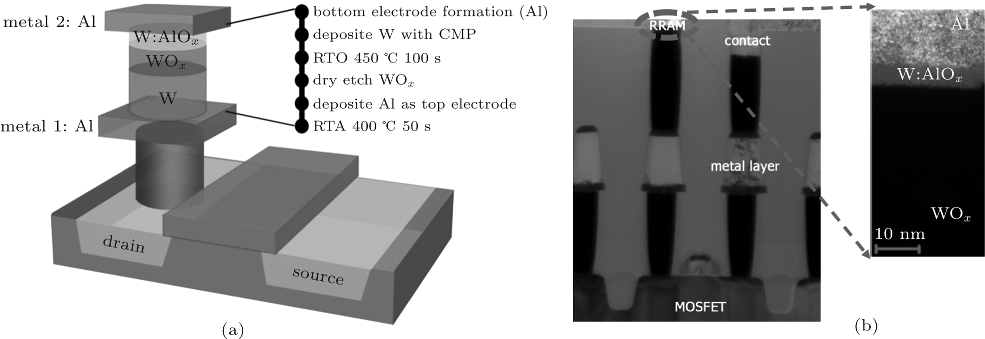 | Fig. 1. (a) Schematic of the W:AlOx/WOy bilayer RRAM device with 1T1R structure and major fabrication steps; (b) cross-sectional TEM images of the 1T1R structure. |
During electrical measurements, positive voltages were applied on the TE while the bottom electrode (BE) was kept as the ground. A Keithley 4200 analyzer was used for pulse measurements and an Agilent B1500A semiconductor parameter analyzer equipped with an ERS SP72 temperature controller was used for DC sweep measurements.
Figure 2(a) shows the DC sweep measurement results where SET and RESET voltages are almost the same. It is hard to tell obvious difference between SET and RESET process based on DC sweep results. In real applications, RRAM is programmed with pulsing bias, and to achieve stable switching, pulse conditions for SET and RESET turned out to be very different. There are more than 3 orders of difference between SET and RESET times. This significant difference cannot be revealed by DC sweep measurements. This large difference in programming time also indicates the switching process differences behind the SET and RESET operations.
 | Fig. 2. (a) DC sweep I– V curves of the fabricated W:AlOx/WOy bilayer RRAM device; (b) pulsed programming measured resistive switching cycles of the fabricated RRAM devices. |
In order to find out the possible physical mechanisms causing this asymmetric in SET and RESET speed, in our measurement pulse electrical tests were varied from amplitude to width and DC sweep electrical tests were performed under different temperatures. During those measurements, only one parameter of test conditions was varied at a time (i.e., other parameters were kept unchanged). The typical pulse measurement conditions are 1.2 V, 80 ns for SET and − 1.1 V, 200 μ s for the RESET operations.
Figure 3(a) shows the test results of varying SET pulse width from 60 ns to 500 ns while other conditions are kept the same. In this case, no obvious changes on the LRS and HRS values were observed. These measurement results suggest the longer time has less impact on the LRS value during the SET operation. Figure 3(b) shows the test results of varying RESET pulse width from 5 μ s to 400μ s. At the beginning, the RESET pulse width increases from 250μ s to 300 μ s, and the HRS values increase from about 5 kΩ to 7 kΩ with longer pulse. Next, the RESET pulse decreases from 300 μ s to 5 μ s and the HRS values follow the RESET pulse width trend and decrease from 7 kΩ to 2.5 kΩ . At the end, the RESET pulse is set back to 400 μ s and the HRS values increase to the highest value of the whole tests. The above electrical measurements are repeatable. Clearly, the HRS value is affected not only by the RESET amplitude, but also by the RESET pulse width strongly. This is in contrast to the SET process where the LRS value is not sensitive to the SET pulse width. Larger pulse width means longer current passing through the RRAM cells which should induce more joule heating locally.
 | Fig. 3. Pulse measurements on W:AlOx/WOy RRAM cells with (a) different SET pulse widths, (b) different RESET pulse widths, (c) different SET pulse amplitudes, and (d) different RESET amplitudes. |
Figure 3(c) shows the measurement results of varying SET pulse amplitude from 1.1 V to 1.3 V while the SET pulse width, RESET pulse amplitude, and width are kept the same. As clearly observed, the low resistance state (LRS) resistance decrease from 3 kΩ to 500 Ω with the increase of the SET pulse amplitude. This indicates a larger electrical field during the SET operation would induce thicker CFs, which cause low LRS. The high resistance state (HRS) values, in the above measurements, decrease from 20 kΩ to 10 kΩ . When the RESET pulse amplitude decreases from 1.2 V to 1.0 V, the HRS values decrease from 30 kΩ to 10 kΩ , as shown in Fig. 3(d). The LRS also decreases from about 3 kΩ to 1 kΩ , although the SET conditions were kept the same.
Changing SET pulse amplitudes, the HRS and LRS resistance were varied with the pulse amplitudes, as shown in Fig. 3(c). By changing the RESET pulse amplitudes, the HRS and LRS resistances are also varied, as shown in Fig. 3(d). These two electrical comparison tests suggest that the electrical field strength is an important factor for both SET and RESET processes. A significant difference based on our experiments is that the RESET operation needs much more time in comparison to the SET process although similar operational voltages are applied. Summarizing the above electrical tests with different pulse conditions, we could conclude that the electrical field plays an important role in both SET and RESET operations; and the pulse width in association with joule heating is a significant driving factor for the RESET process, but not for the SET process.
To further understand the roles of thermal effects in the resistive switching processes, joule heating generated by external electrical stimuli in Fig. 3 were calculated. To simplify calculations, the following equations are adopted:


Here, QR and QS represent the joule heating generated during RESET and SET process, respectively, VR and VS are the RESET voltage and the SET voltage, RL and RH are the LRS resistance and the HRS resistance, tR and tS are the RESET pulse width and the SET pulse width.
The calculated joule heating values are listed in Table 1. From Table 1, for stable resistive switching, joule heating generated in the RESET process is 4– 5 orders higher than that generated in the SET process. These simple calculations also support that thermal effect has more influence on the RESET process than on the SET process.
| Table 1. Calculated joule heating in RRAM cell due to external electrical stimuli. |
In order to further understand the thermal effect on the SET and RESET processes, temperature-dependent DC sweep measurements were performed on the fabricated W:AlOx/WOy RRAM cells. Figure 4(a) shows the typical DC I– V curves of an RRAM device under different temperatures. Figures 4(b) and 4(c) show the details of the SET/RESET switching part. This RRAM cell was operated under the temperatures from 253 K to 403 K. As the temperature increases, the SET voltage shows random variation in the range of 0.70– 0.85 V. However, the RESET voltage shows consistent decrease from 0.90 V to 0.65 V. Here, the SET/RESET voltages are defined as the sweep voltage when the cell resistance starts to change. We conclude that high ambient temperature is helpful for the RESET operation.
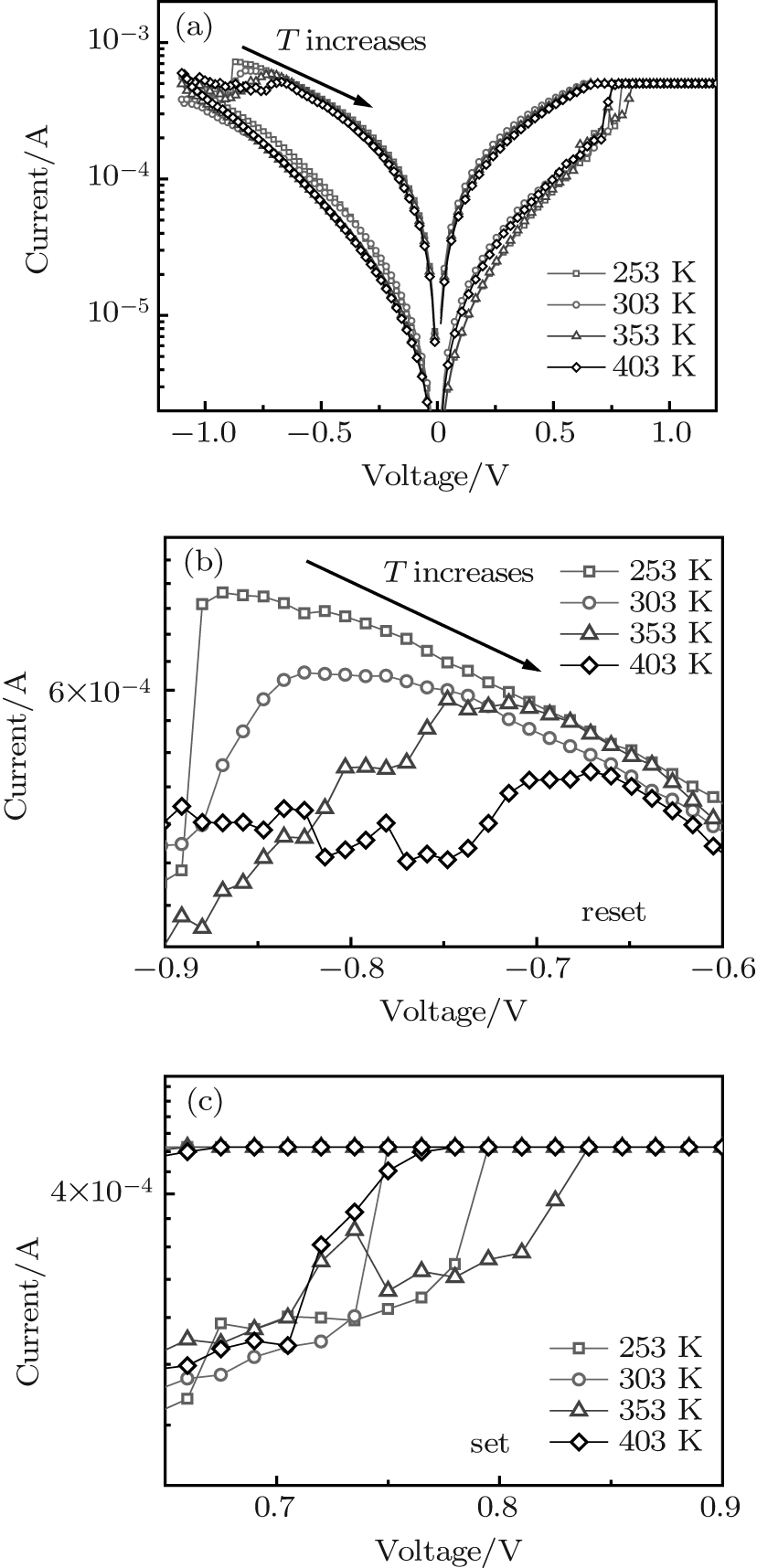 | Fig. 4. The W:AlOx/WOy bilayer RRAM device is operated at different ambient temperatures. (a) DC I– V sweep under different temperatures; (b) zoom in graph of the RESET switching region; (c) zoom in graph of the SET switching region. |
This further supports that the RESET process requires more joule heating to start the switching process. The reason is probably due to the fact that higher device temperature makes it easier for oxygen ions to escape from the chemical bond and migrate back to fill the oxygen vacancies and to rupture the conductive filament. Recent studies on the TaOx RRAM system also showed that the RESET voltages decrease with increasing device temperature.[19]
A redox reaction model is proposed to explain the phenomenon that joule heating plays an important role in the RESET operation. In the Al/W:AlOx/WOy/W RRAM cell, some oxygen ions form W– O bonds and some form Al– O bonds in the W:AlOx layer. During the SET operation, a positive voltage is applied on the TE of the cell, oxygen ions will break from original chemical bonds and migrate to TE under the electrical field. Oxygen vacancies could form CFs in the resistive switching layer and switch the RRAM cell to LRS.
The Gibbs free energy of forming WO3 is – 764.1 kJ/mol in comparison to – 1582.3 kJ/mol for Al2O3. The Gibbs free energy indicates how easy the redox reaction happens.[20] In this case, the value of Gibbs free energy tells how easy the metal could be oxidized. More negative Gibbs free energy means the oxidation process is more preferred. It is expected that most of the oxygen ions are from W– O bonds broken during the forming and SET operations since Al– O bonds are stronger than W– O bonds. Oxygen ions from W– O bonds migrated to Al TE and leave oxygen vacancies formed CFs. This completes the resistive switching from HRS to LRS, as shown in Fig. 5(a). Those oxygen ions migrate to Al TE and would partially oxidize the Al and form Al– O bonds. Based on the experimental data, the electrical field under the SET condition is strong enough to make this process happen.
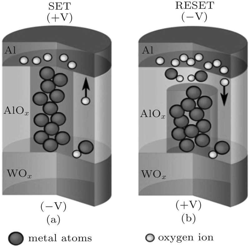 | Fig. 5. (a) During the SET process, oxygen ions migrate to Al TE and partially oxidize the Al TE. (b) During the RESET operation, under both electrical field and thermal process, the oxygen ions broken from Al– O bonds or locally thermal generated in the switching layer could rupture the CFs. |
The RESET process needs to force the oxygen ions to migrate to the W:AlOx resistive switching layer and recombine with the oxygen vacancies. This would rupture the CFs and take the cell back to HRS, as shown in Fig. 5(b). In the RESET process, the oxygen ions could come from breaking Al– O bonds in the TE layer, or generation from the surrounding area due to joule heating. To break Al– O bonds, as Gibbs free energy data has shown, much more energy is required in comparison to breaking W– O bonds during SET operation. Where can we get that high energy? A longer pulse width would generate lots of joule heating locally, and a higher local temperature will significantly reduce the barrier of breaking Al– O bonds. This means a longer pulse width is favorable for the RESET process. The second path, to generate oxygen ions from the surrounding area by joule heating, a significant amount of joule heating is also needed to bring the local temperature high enough for the thermal generation process to happen. A longer pulse width is also needed to heat up locally and raise the local temperature. A higher ambient temperature is also favorable for Al– O bonds broken and requires less RESET voltages.
The asymmetric redox reaction is the cause of the large difference between SET and RESET times. During the SET operation, weak W– O bonds in the W:AlOx layer could be broken under the SET electrical field. In contrast, for the RESET operation, a longer pulse is necessary to generate enough joule heating to raise the local temperature which is favorable for Al– O bonds broken or thermal generation of oxygen ions locally.
Large difference between the SET and REST pulse width was observed in Al/W:AlOx/WOy/W bilayer RRAM devices. The RESET pulse width is 3– 4 orders longer than the SET case. Various pulse measurements and DC sweeping under different temperatures were carried out to further understand the cause of this phenomenon. An asymmetric redox reaction is believed to be the reason. During the SET operation, weak W– O bonds in the W:AlOx switching layer could be broken under an electrical field. In the RESET process, a longer pulse time is needed to raise up the local temperature which is favorable for breaking Al– O bonds in TE or generating oxygen ions through the thermal generation process.
| 1 |
|
| 2 |
|
| 3 |
|
| 4 |
|
| 5 |
|
| 6 |
|
| 7 |
|
| 8 |
|
| 9 | [Cited within:1] |
| 10 |
|
| 11 |
|
| 12 |
|
| 13 |
|
| 14 |
|
| 15 |
|
| 16 |
|
| 17 |
|
| 18 |
|
| 19 |
|
| 20 | [Cited within:1] |