2. Theoretical model description and simulation resultsThe physical parameters of Ge1− xSnx or SixGe1− x − ySny can be obtained using the linear interpolation formulae, excluding the band-gap. There is a nonlinear relationship between alloy band-gap  and the alloy composition x. As far as Ge1− xSnx alloys are concerned, the band-gap is usually calculated by a parabolic function, which is listed as follows:

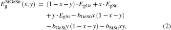
where x is the Sn percentage, y is the Si percentage, and b is bowing parameter.
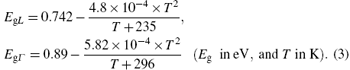
For a Ge1− xSnx alloy, bL = 0.89[8] and bΓ = 2.1[11] are cited from the latest result; for GeSi and SiSn, bΓ = 0.21 and 13.2, [15] respectively. Figure 1(a) shows the direct band-gap Eg, Γ and indirect band-gap Eg, L of Ge1− xSnx alloy, each as a function of Sn percentage at room temperature. The band parameters of Si, Ge, and Sn are cited from the data handbook.[16] In order to obtain a more precise result the temperature-dependence of the Ge band-gap is taken into account (that of Sn is neglected because of its low percentage), as follows:[17]
As figure 1(a) shows, when x (Sn) equals 7.8%, the direct and indirect band-gap reach the same value (about 0.56 eV). Based on this model, the band parameters of Ge1− xSnx alloys, with x in a range between 0% and 15% (0%, 3%, 6%, 7.8%, 10%, 12%, and 15% are chosen in the calculation) are calculated and then utilized for the next optical simulations.
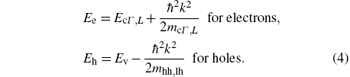
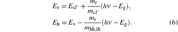
The E– k relation between electron and hole are assumed to be parabolic, as follows:
And the photon energy hν emitting through Γ – h transition is given as follows:
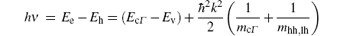

According to Eq. (5), the electron energy in the Γ valley Ee and hole energy Eh are described by
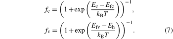
In a steady state, electrons and holes obey quasi-Fermi distribution, which is described by electron quasi-Fermi level Efc and hole quasi-Fermi level Efv. When the energy difference between an electron (Ee) and a hole (Eh) with the same k in the reciprocal space is equal to photon energy E = hν , the occupation probabilities of an electron and a heavy hole are described, respectively, by
Quasi-Fermi level values (Efc and Efv) corresponding to injected carrier density Ninj = Pinj and doping density ND under a degenerate condition (with heavy doping and high injection) can be obtained by the calculation method from the second chapter of Ref. [18] through the following relationship:

The percentage of electrons occupying Γ band valley can then be obtained as

Compared with the direct Γ band valley, the indirect L band valley of Ge or Ge1− xSnx can accommodate a majority of electrons because of its lower energy valley, high degeneracy (s = 4), and the bigger effective mass of the electron. Even worse, the electron in the indirect L band valley has a very low emission transition probability and high contribution of free-carrier absorption. While the key point for the laser process is to achieve considerable stimulated radiation from a direct Γ valley, the indirect L band valley has a serious negative influence on this material luminescence quantum efficiency.
Figure 1(b) shows the percentage of electrons occupying the Γ band valley of Ge1− xSnx with x value being between 0% and 15% (n-doping density: 1 × 10¹⁸/cm3, injected carrier density is 1 × 1019 cm− 3; room temperature: 300 K). It is indicated that the percentage of electrons occupying the Γ band valley of Ge0.88Sn0.12 is 1000 times as high as that of Ge; however, that of pseudo-direct band Ge0.922Sn0.078 alloy is still only about 1%, as shown in Fig. 1(b).
After the calculation of band structure and carrier distribution, the optical gain spectrum (gΓ − hh) and the spontaneous emission spectrum (RspΓ − hh) through Γ – hh radiative recombination can be obtained; the formulae are given as follows:[19]


where e is the electron charge, m0 is the free electron mass, ɛ 0 is the permittivity of vacuum, h is the Planck constant (ħ = h/2π ), c is the speed of light in vacuum, n0 is the index of refraction, mcΓ is the effective mass of electron in Γ band valley, mhh is the heavy hole mass, mlh is the light hole mass, Eg is the band gap, and  is the average matrix element for the Bloch states.
The optical gain spectrum gΓ − lh and the spontaneous emission spectrum RspΓ − lh through Γ – lh radiative recombination can be obtained in a similar way, i.e., just replacing mhh in Eqs. (10) and (11) with mlh. Thus, the total optical gain spectrum G (hν ) and the spontaneous emission rate Rsp are given as follows:


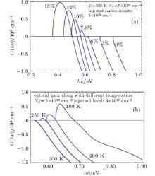
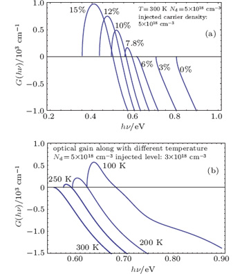
The total optical gain spectra of Ge1− xSnx with different Sn percentages and with a same injected carrier density (5 × 10¹⁸/cm3) and doping density (5 × 10¹⁸/cm3) at room temperature are then calculated and shown in Fig. 2(a). The optical gain significantly increases with the increase of Sn percentage. The maximal gain coefficient of Ge1− xSnx alloy increases from 200/cm (x = 7.8%) to 1000/cm (x = 15%), which indicates that the introduction of Sn into Ge can promote optical gain evidently and may reduce threshold carrier density. The decrease of threshold carrier density also reduces the FCA and Auger recombination process, which will further lower the threshold current density.
Optical gain spectra of alloy with 7.8% Sn (injected carrier density: 5 × 10¹⁸/cm3, n-doping level: 3 × 10¹⁸/cm3) at different temperatures are simulated. As figure 2(b) indicates, it is hard for Ge0.922Sn0.078 to realize optical amplification at 300 K under this carrier density condition, but a low temperature can improve optical gain effectively and the maximal gain can reach 500 cm− 1 at 100 K. The blue shift of maximal gain is due to the band-gap broadening at low temperatures.
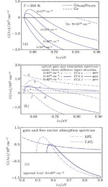
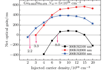
The optical gain spectra of a Ge0.922Sn0.078 alloy with four different injected carrier densities are also studied (n-doping concentration: 5 × 10¹⁸/cm3, and temperature: 300 K), as shown in Fig. 3(a). Although Ge0.922Sn0.078 has become a direct band-gap semiconductor, a high injection density, such as 6 × 10¹⁸/cm3, is needed to achieve population inversion in direct Γ band valley and provide significant positive optical gain. In addition, a comparison between Ge0.922Sn0.078 and Ge with an identical injected carrier density of 9 × 10¹⁸/cm3 is made. It is indicated by the dashed line and solid line in Fig. 3(a) that the maximum gain of Ge0.922Sn0.078 can reach 500 cm− 1, while the optical gain of Ge is still negative.
It is obvious that high injection could contribute to the achievement of high optical gain; however, the FCA effect is considerable in high doping or at a high injection level, which is bad for optical gain. The FCA effect, consisting of the absorptions of L-conduction valleys, Γ -conduction valley, heavy-hole band, and light-hole band, can be described by Drude– Lorentz equation[20] as follows:
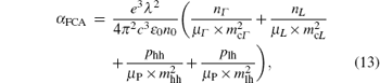
where λ is the free space wavelength; nΓ and nL are the electron densities in the Γ - and L-conduction valleys, respectively; phh and plh are the hole densities in the heavy and light valence band, respectively; mcΓ and mcL are the electron effective mass values of the Γ - and L-conduction valleys, respectively; mhh and mlh are the heavy and light hole effective masses; μ L and μ Γ are the electron mobilities in the L- and Γ -conduction valleys, respectively; and, μ P is the hole mobility in the valence band.
Moreover, the Ge1− xSnx carrier mobility (μ L, μ Γ , and μ P) dependences of temperature and carrier density could be estimated by that of Ge for simplicity. The motilities in undoped Ge at the values of temperature T (100 K– 300 K) are given by[16]

In addition, the mobility is also carrier-concentration-dependent, and the electron mobility of L-conduction valley and hole mobility of Ge (electron density of L-conduction valley: nL, and hole density: np) at 300 K is given by[21, 22]
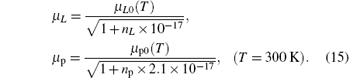
The above equations are extended to other temperatures reasonably, and equation (14) is substituted into Eq. (15) to obtain μ L(n, T) and μ p(p, T) each as a function of carrier density n and p (in cm− 3) at T (in K). However, to date there are no experimental data about the mobility of electrons the in Ge Γ -conduction valley. The relationship like Eq. (16) and Eq. (17) is then assumed to be

Finally, the FCA spectra of Ge1− xSnx alloys as a function of carrier density and temperature can be obtained through Eqs. (13)– (17). For the optimization of injection density, the optical gain and FCA spectra of the Ge0.922Sn0.078 alloy are simulated simultaneously with injected carrier densities of 5 × 10¹⁸, 9 × 10¹⁸, and 2 × 1019 cm− 3, respectively. The net gain is defined to simplify the description as follows:

As shown by the three curves b, d, f in Fig. 3(b), α FCA is inversely proportional to (hν )2 and increases with the increase of carrier density. Moreover, gnet (hν ) is negative for the photon energy between 0.55 eV and 0.90 eV when the injected carrier density is 5 × 1018 cm− 3, as shown by curve e and curve f in Fig. 3(b); when the density goes to 9 × 1018 cm− 3, gnet(hν ) is positive within a certain value range of photon energy, as shown by curve c and curve d; when the injected carrier density reaches 2 × 1019 cm− 3, gnet(hν ) is negative again, as shown by curve a and curve b. So it is concluded that the injected carrier density is not better higher, there should be an optimal injection to reach a maximal net gain for a special wavelength. In addition, as shown in Fig. 3(c), the comparisons of G(hν ) and α FCA between Ge0.922Sn0.078 and Ge0.9Sn0.1 with the same injection level indicate that the FCAs of both alloys almost coincide but the maximal optical gain value of Ge0.9Sn0.1 alloy is much higher than that of Ge0.922Sn0.078.
In a real device simulation, when the G (hν ) and α FCA(hν ) of the active layer are obtained, the device threshold carrier density nth can be obtain from the following equation at a given wavelength (hν ):

where Γ is the confinement factor, α i is the internal loss, mainly including FCA (α i ∼ α FCA), α m is the mirror loss, L is the cavity length, R1 and R2 are the reflectivities of the front and back mirror, respectively. When the net optical gain

is positive, which means that the optical gain can overcome the loss, the lasing can occur.
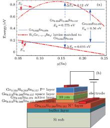
In this real device simulation, Ge0.922Sn0.078 is chosen as an active region because it is difficult to achieve the high Sn percentage alloy by the epitaxy technique.[23] In order to obtain high injection efficiency and low threshold current density, a double heterojunction (DHS) diode is designed. Figure 4(a) shows the band-gap and band-offset of Ge1− x − ySixSny cladding layer (lattice-matched to Ge0.922Sn0.078 active region), each as a function of Sn percentage y. For well confining the carriers and light, the cladding layer of Ge0.554Si0.289Sn0.157 (y = 0.157) can have the largest band-gap difference with Ge0.922Sn0.078 layer: Δ Eg = 215 meV, valence-band-offset Δ Ev = 95 meV and conduction-band-offset Δ Ec = 120 meV. The DHS laser device as shown in Fig. 4(b) is designed. In the next device simulation, α m is assumed to be 10 cm− 1 and Γ is assumed to be 1.
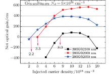
The Gnet(hν ) spectrum of Ge0.922Sn0.078 alloy (doping density: 5 × 1018 cm− 3) as a function of injection level is calculated at a given wavelength of λ , the threshold carrier density nth can then be obtained where Gnet(hν ) equals zero. The net gain spectra of three different wavelengths, each as a function of injected carrier density, are shown in Fig. 5, and the arrow-marked threshold carrier densities are about 8 × 1018 cm− 3 (temperature: 300 K, and λ = 2100 nm), 2.2 × 1018 cm− 3 (temperature: 200 K, and λ = 2050 nm), and 3.3 × 1018 cm− 3 (temperature: 200 K, and λ = 2000 nm), respectively. Gnet(hν ) at room temperature is much smaller than at 200 K. In addition, the maximal values of Gnet(hν ) of these three conditions all appear at about n ∼ 9 × 1018 cm− 3.
The the injected threshold current density Jth corresponding to threshold carrier density nth can then be estimated according to the following formula:

where η i is the injection efficiency, and assumed to be 0.8; d is the depth of active region, and assumed to be 10 μ m: Rsp is the spontaneous emission rate (as Eq. (12)), and RAug is the Auger recombination rate, which is neglected at 200 K when considering that the Auger recombination coefficient of Ge0.922Sn0.078 is small at low temperatures (there is no report at present). However, the RAug of Ge0.922Sn0.078 at room temperature is estimated through using Auger recombination coefficients of Ge, as shown in Eq. (22), which are Cppn = 7.0 × 10− 32 cm6/s[24] and Cnnp = 3.0 × 10− 32 cm6/s.[25]
The corresponding values of Jth are then obtained through Eqs. (12), (21), and (22), respectively, as 6.47 kA/cm2 (temperature: 200 K, and λ = 2050 nm), 10.75 kA/cm2 (temperature: 200 K, and λ = 2000 nm), and 23.12 kA/cm2 (temperature: 300 K, and λ = 2100 nm). All of the above simulation results are shown in Table 1. These results indicate the possibility of obtaining a GeSn short-wave infrared laser at room temperature.
Table 1.
Table 1.
 Table 1. Threshold carrier densities, spontaneous emission rates, Auger recombination rates, and threshold current densities at different temperatures and wavelengths.| Temperature/K | Wavelength/nm | nth/cm− 3 | Rsp/cm− 3· s− 1 | RAug/cm− 3· s− 1 | Jth/(kA/cm− 2) |
|---|
| 200 | 2000 | 3.3 × 10¹⁸ | 5.37 × 1025 | neglected | 10.75 | | 200 | 2050 | 2.2 × 10¹⁸ | 3.23 × 1025 | neglected | 6.47 | | 300 | 2100 | 8.0 × 10¹⁸ | 1.14 × 1026 | 1.12 × 1024 | 23.12 |
| Table 1. Threshold carrier densities, spontaneous emission rates, Auger recombination rates, and threshold current densities at different temperatures and wavelengths. |


 , Xue Chun-Lai, Zhang Xu, Cong Hui, Liu Zhi, Zhang Guang-Ze, Wang Qi-Ming]