Fabrication and characterization of novel high-speed InGaAs/InP uni-traveling-carrier photodetector for high responsivity
Chen Qing-Tao, Huang Yong-Qing†

, Fei Jia-Rui, Duan Xiao-Feng, Liu Kai, Liu Feng, Kang Chao, Wang Jun-Chu, Fang Wen-Jing, Ren Xiao-Min
Institute of Information Photonics and Optical Communications, Beijing University of Posts and Telecommunications (BUPT); State Key Laboratory of Information Photonics and Optical Communications (BUPT), Beijing 100876, China
†Corresponding author. E-mail: yqhuang@bupt.edu.cn
*Project supported partially by the National Natural Science Foundation of China (Grant Nos. 61274044 and 61077049), the National Basic Research Program of China (Grant No. 2010CB327600), the Program of Key International Science and Technology Cooperation Projects, China (Grant No. 2011RR000100), the 111 Project of China (Grant No. B07005), the Specialized Research Fund for the Doctoral Program of China (Grant No. 20130005130001), and the Natural Science Foundation of Beijing, China (Grant No. 4132069).
1. IntroductionHigh performance photodetectors are of great importance for developing future high-speed, large capacity optical communication, signal processing and measurement systems.[1] However, in conventional PIN photodetectors, the photo-generated electrons and holes in the depleted absorption layer produce space charge effect due to charge buildup, which causes degradation of the high-speed response of a photodetector at high current level and simultaneously makes the responsivity down. To overcome the space charge effect and achieve high speed response, several successful devices structures have been proposed, such as uni-traveling-carrier photodiodes (UTC-PDs), [2, 3] a partially depleted absorber photodiode, [4] a velocity-matched distributed photodiode, [5] and a non-uniform doped collector UTC-PD.[6] Meanwhile, in order to obtain high responsivity, high output power and high 3-dB bandwidth, the modified UTC-PDs[7– 9] with slightly n-type-doped InP depletion layer acting as charge compensation were reported. Further increase of the saturation current, even higher, of the device, a modified UTC-PD incorporating a cliff layer before the collection layer was proposed.[10] The collapse of the electric field in the absorption layer is another reason for leading to the saturation characteristics of the device.[11– 13]
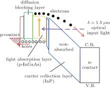
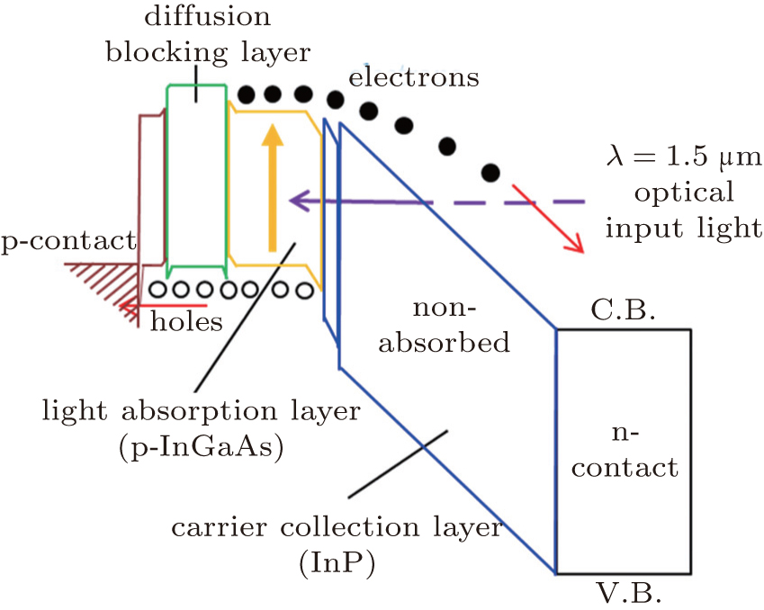
It is well known that UTC-PD structures are all composed of an un-depleted p-type photo-absorption layer and a wide-gap depleted electron-collection layer, [2] and its band diagram is shown in Fig. 1. The photo-generated carriers, which are minority electrons injected into the collection layer at the same time and act as active carriers for enhancing saturation output current whereas majority holes do not act as active carriers, are produced in absorption layer of UTC-PDs.
One advantage of this type of structure is that it has a single carrier, namely electrons whose velocities are greater than those of holes in the drift region, thus greatly reducing the space charge effect, so UTC-PD integrate three remarkable features, i.e., high speed, high saturation output, and low operating bias voltage.[2, 3] In spite of achieving high speed response, lower responsivity (equivalently quantum efficiency) is another difficult problem to resolve. Therefore, modified UTC-PDs with partially depleted absorption layers[7– 9] to increase the responsivity and high saturation current were investigated. A 40-μ m diameter device showed a responsivity of 0.75 A/W and a saturation current of 130 mA.[9]
In this paper, we propose an InGaAs/InP uni-traveling-carrier photodetector (UTC-PD) that employs Gaussian graded doping in InGaAs absorption layer and InP depleted layer to optimize the device performance. Afterwards, the responsivity values of a 40-μ m diameter device are 0.854 A/W and 1.071 A/W (namely the quantum efficiency of 68.51% and 86%) at reverse bias voltages of 9 V and 10 V, respectively. The 3-dB bandwidth is only 11 GHz under a reverse bias voltage of 3 V due to the higher absorption layer thickness and the larger device area.
2. Device growth and fabrication2.1. Device growth and analysisThe growth of UTC-PD is realized in a Thomas Swan 3 × 2-inch (1 inch = 2.54 cm) closely coupled showerhead (CCS) low-pressure metal-organic chemical vapor deposition (LP-MOCVD) system with a fixed reactor pressure of 100 Torr (1 Torr = 1.33322 × 10² Pa) and the total flow rate of 1.2 × 10⁴ sccm.[14, 15] High-purity trimethylgallium (TMGa), trimethylindium (TMIn), pure arsine (AsH3), and phosphine (PH3) are used as precursor materials. The carrier gas is pd-cell purified hydrogen (H2). Silane (Si) and diethylzinc (Zn) serve as the n-type and the p-type dopant sources, respectively. The 2-inch (100)-oriented semi-insulating InP wafer with Fe-doped is used as the substrate.
The detailed parameters of epitaxial wafer structure are shown in Table 1. Firstly, the InP wafer is cleaned by a chemical method: it is loaded into the reactor chamber of an LP-MOCVD system and baked at 220 ° C for 600 s, and then thermally cleaned at 650 ° C for 300 s in arsine and hydrogen ambient.[14, 15] Afterwards, the wafer is cooled down to 450 ° C, and then the 200-nm low-temperature (LT) InP buffer layer which has the ability to accommodate the misfit strain, is grown by incorporating Si-doped concentration of 1.00 × 1019 cm− 3.[14] Secondly, an 20-nm InGaAs etch-stopping layer is grown on LT InP buffer layer at a normal temperature of 650 ° C with Si-doped concentration of 1.00 × 1019 cm− 3.
Table 1.
Table 1.
 Table 1. Epitaxial structure of the UTC-PD.| Material | Doping/cm− 3 | Thickness/nm | Layer |
|---|
| p-In0.53Ga0.47As | 2.00 × 10¹⁹ | 50 | p contact layer | | p-InP | 1.50 × 10¹⁸ | 900 | diffusion blocking layer | | p- In0.53Ga0.47As | 1.50 × 10¹⁷ ∼ 4.00 × 10¹⁸ (Gaussian doping) | 640 | un-depleted absorption layer | | un- In0.53Ga0.47As | 6.00 × 10¹⁶ | 200 | depleted absorption layer | | un-In0.72Ga0.28As0.6P0.4 | 3.00 × 10¹⁶ | 10 | transition layer | | un- In0.89Ga0.11As0.23P0.77 | 3.00 × 10¹⁶ | 10 | transition layer | | n-InP | 2.50 × 10¹⁶ ∼ 5.00 × 10¹⁸ (Gaussian doping) | 500 | depletion layer | | n-InP | 5.00 × 10¹⁸ | 1065 | n contact layer | | n- In0.53Ga0.47As | 1.00 × 10¹⁹ | 20 | etch-stopping layer | | n-InP | 1.00 × 10¹⁹ | 200 | buffer layer | | S. I. – InP substrate |
| Table 1. Epitaxial structure of the UTC-PD. |
Following the etch-stopping layer, a 1785-nm collection layer is grown. It consists of a 1065-nm InP layer grown at 650 ° C with an Si-doped concentration of 5.00 × 1018 cm− 3 which realizes the high quality InP/InGaAs heteroepitaxy growth and a 720-nm depletion layer. The 720-nm depletion layer is comprised of a 500-nm InP layer, two 10-nm-thick InGaAsP transition layers and 200-nm InGaAs depleted absorption layer, which are all grown at 650 ° C. The 500-nm InP layer involving Si-Gaussian graded doping concentration from 5.00 × 1018 cm− 3 down to 2.50 × 1016 cm− 3 is achieved to have the charge compensation function.[7] The two 10-nm-thick InGaAsP transition layers each with a slightly doping concentration of 3.00 × 1016 cm− 3 are used to smooth the abrupt conduction band carrier at the InGaAs/InP heterojunction interface and compensate for the space charge.[7] The 200-nm InGaAs depleted absorption layer with an Si-doped concentration of 6.00 × 10¹⁶ is adopted.
Thirdly, a 640-nm InGaAs absorption layer is grown at 650 ° C by incorporating Zn-Gaussian graded doping concentration from 1.50 × 1017 cm− 3 to 4.00 × 1018 cm− 3 to form a quasi-electric field to aid carrier transport in the absorption layer.[7– 9] Then, in order to produce a diffusion blocking layer adjacent to InGaAs absorption layer, a thicker (about 900 nm) InP blocking layer is grown at 600 ° C with a Zn-doped concentration of 1.50 × 1018 cm− 3 to block minority electrons from diffusing toward the top p-contact surface. Finally, a 50-nm InGaAs layer is grown at 550 ° C, containing a heavily Zn-doped concentration of 2.00 × 1019 cm− 3 acting as Optimal ohmic p-type anode contact layer. Therefore, the growth of UTC-PD wafer is completed.
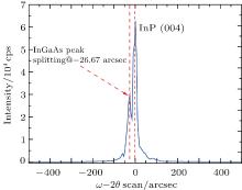
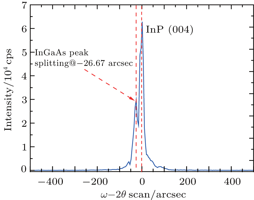
2.2. DCXRD measurementHigh resolution double crystal x-ray diffraction (DCXRD) ω – 2θ scans applied to the symmetric (004) reflection are performed to determine the compressive strains of the UTC-PD sample. The DCXRD ω – 2θ scan rocking curve of the UTC-PD is shown in Fig. 2. The peak splitting is defined as the angular splitting between the main InGaAs layer peak and the InP substrate peak. The InGaAs peak splitting is shifted leftwards from the InP substrate peak, suggesting that it has a larger lattice constant than that of InP, is – 26.67 arcsec. The mismatch between InP and InGaAs is 104.9 ppm, indicating that the UTC-PD sample is a high-quality wafer.
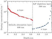
2.3. ECV measurementThe doping concentrations of the device with a 640-nm InGaAs absorption layer and a 500-nm InP depletion layer are measured by electrochemical capacitance-voltage profiler (ECV). The ECV measurement electrolyte is chosen as diaminoethane EDTA which consists of anhydrous ethylenediamine, ethylenediaminetetraacetic acid (EDTA)[16] and deionized water prepared according to a certain proportion. Finally, a few drops of Triton X100 are added to remove the bubbles of diaminoethane EDTA electrolyte. The ECV measurement result is shown in Fig. 3.
The measured doping concentration of p-type InGaAs absorption layer ranges from 4.00 × 1018 cm− 3 down to 1.50 × 1017 cm− 3 that presents a trend toward gradual wane. Meanwhile, some breakpoints occur due to the adjustments of the I– V and C– V curves in the test process. On the contrary, the doping concentration of n-type InP depletion layer, which shows a bigger trend gradually ranges from 2.50 × 1016 cm− 3 to 5.00 × 1018 cm− 3. The two-doping shapes constitute an inverted Gaussian distribution which first assists electron transport faster, and then reduces the junction capacitance (namely the resistance capacitance component) in order to increase the bandwidth of the UTC-PD device.
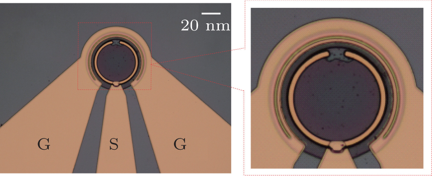
2.4. Device fabricationThe UTC-PD is fabricated by wet-chemical etching by using the following procedures. Firstly, the sample is cleaned with acetone, ethanol and deionized water, respectively. Then, a Pt/Ti/Pt/Au (= 20 nm/20 nm/20 nm/180 nm) layer is deposited successively on top p-type contact capping layer and patterned by a lift-off process to form an enclosed circular mesa-structure instituted as a p+ ohmic contact with an inner diameter of 40 μ m. Secondly, a protection for 42-μ m diameter p+ ohmic contact outside edge is constructed by using circular lithographic cover templates, and then the InGaAs, InP, and InGaAsP layers are etched by H2SO4:H2O2:H2O = 1:1:10, H3PO4:HCl = 3:1, and H2SO4:H2O2:H2O = 3:1:1 several times to form n-type InP contact layer, so the n+ ohmic contact is achieved by a Pt/Ti/Pt/Au (= 20 nm/20 nm/20 nm/180 nm) lift-off. Afterward, the wafer is cleaned with acetone to remove the extra Pt/Ti/Pt/Au layer deposited with photoresist, then the wafer is cleaned with ethanol and deionized water seven times until no left-impurity exists. Therefore, p and n circular metal contact-base are fabricated.
Following the above procedures, a thermal cycle annealing process is performed from 0 ° C to 160 ° C then back to 0 ° C in nitrogen ambient after the sample has been covered with polyimide:N, N-dimethylacetamide (= 4:1) for pre-passivation. Afterward, the top windows of the sample are opened and this makes its surface passivated from 0 ° C to 250 ° C and then back to 0 ° C in nitrogen ambient in order to make the p and n circular metal firmly stable on the InP substrate. Finally, a Ti/Au (= 120 nm/300 nm) interconnect metal, which forms the coplanar electrodes on the top of the polyimide layer, is deposited. The high-speed response, photocurrent, and dark current characteristics of those three coplanar pads forming ground-signal-ground (GSG) structure, that is to say, N electrode, P electrode, and N electrode, are easy to measure. The top view optical micrograph of the fabricated UTC-PD is shown in Fig. 4.
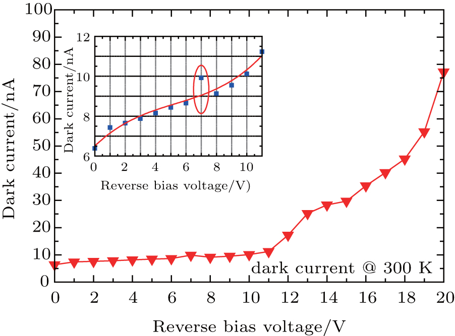
3. Results and discussion3.1. Dark currentUnder a temperature of 300 K, the current– voltage characteristic of the UTC-PD is measured as shown in Fig. 4. The results show that the dark current is below 11.5 nA (see the inset graph of Fig. 5) in the case of the reverse bias voltage ranging from 0 V to 11 V and then increases quickly when the reverse bias voltage is larger than 10 V for a 40-μ m diameter UTC-PD. There is about 8.83% test error of the dark current at the 7 V reverse bias voltage (the point of the elliptical ring in the inset graph of Fig. 5) in the test process due to several test accessories, such as the longer fiber length, the worn connecting heads of test fiber, and the calibration of the test equipment.
As is well known, the factors of generating dark current mainly result from the imperfect passivation of the device surface, [17] diffusion current, generation recombination current caused by the background dopant and the density of the dislocations, [18] tunneling current at the high reverse bias voltage, [19] and surface leakage.[20] Therefore, some scientific and reasonable methods, such as perfect passivation, smooth and residue free surface, and anisotropic etching profile have been adopted to reduce surface leakage current and the sidewall current so as to improve the integrated performance of the UTC-PD device.
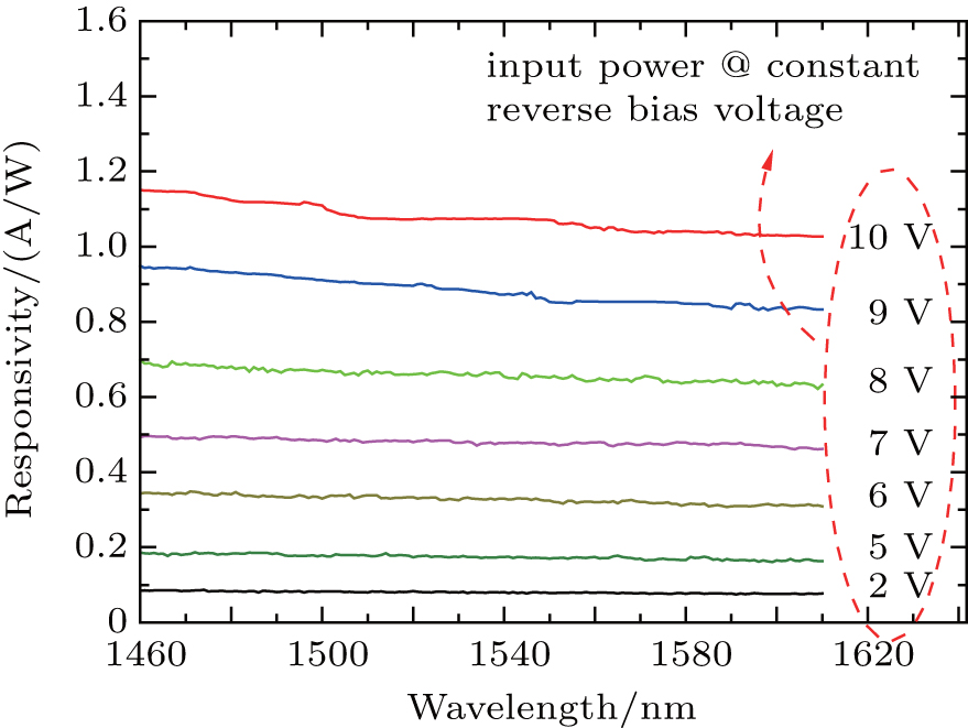
3.2. ResponsivityIn order to measure the responsivity of UTC-PD, an Anritsu Tunics SCL tunable laser with a single-mode fiber pigtail as a light source is employed during the test. The UTC-PD is illuminated vertically by an input light beam of 1-mW optical power from the top side. The whole test process is under a stable temperature of 300 K. According to the test photocurrent, the dark current and the optical power, we can calculate the responsivity values with different reverse bias voltages, such as 2 V, 5 V, 6 V, 7 V, 8 V, 9 V, and 10 V as shown in Fig. 6.
The responsivity values of this UTC-PD structure are 0.854 A/W and 1.071 A/W (about 68.51% and 86% of the quantum efficiency) with reverse bias voltages of 9 V and 10 V at a wavelength of 1550 nm. As is well known, the responsivity is related to the area of the effective aperture of the UTC-PD and can be increased by optimizing the antireflection coating material and the thickness of absorption layer. Adopting waveguide structure or backside-illuminated method can also increase the responsivity efficiency of the UTC-PD.[21]
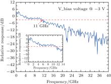
3.3. The 3-dB bandwidthThe frequency response bandwidth of the UTC-PD is measured by a tunable laser and an Agilent E8363C network analyzer in a range from 10 MHz to 40 GHz. The connection of the UTC-PD is the assistance of a microwave probe having 50-Ω characteristic impedance and biased through an internal bias tee. The measured frequency response of the UTC-PD device is shown in Fig. 7, in which the 3-dB bandwidth is 11 GHz with a reverse bias voltage of 3 V as for a 40-μ m diameter UTC-PD, respectively.
The bandwidth value in this paper is lower than that of previously reported photodiodes[9] due to the conduction band discontinuity, the new design doping method, the doping concentration of the collection layer, and the over-corrosion of the top P contact layer in the fabricated process. So, in the future we can reasonably improve the doping concentration and doping method of the collection layer in order to eliminate the conduction band discontinuity and enhance the fabrication level of the UTC-PD device for a higher bandwidth.
It is found that the thickness of the absorption layer, the transit time of the carriers and the resistance capacitance time constant significantly influence the 3-dB bandwidth of the UTC-PD device. Reducing the thickness of the absorption is an important method to obtain higher bandwidth of the UTC-PD. However, this method will result in the decrease of quantum efficiency and responsivity of the UTC-PD device. Therefore, many kinds of optical coupling technologies have been explored to increase the response speed, such as evanescently coupled multimode waveguide UTC-PD, [22] edge-illuminated UTC-PD, [23] micro-ring-based UTC-PD, [24] quadruple 50-Ω coplanar lines (an equivalent 12.5-Ω load) consisting of coplanar waveguides UTC-PD, [25] and so on.
4. ConclusionsIn the present paper, a novel high-speed InGaAs/InP UTC-PD with high responsivity is designed and fabricated. Throughout the measurement, we can find that the UTC-PD structure can provide a maximum responsivity of 1.071 A/W (about 86% of the quantum efficiency at 1550-nm wavelength) at a reverse bias voltage of 10 V. A 3-dB bandwidth of 11 GHz and a dark current of 7.874 nA are obtained at a reverse bias voltage of 3 V for a 40-μ m diameter device. The reasons for affecting the bandwidth of the device are the layer structure, the doping concentration, the fabricated technology level, the thickness of the absorption layer, and the active area. Therefore, we reduce the active region area and the thickness of absorption layer, and optimize the fabrication technology methods to increase the device 3-dB bandwidth. In addition to increasing the bandwidth of the device, we can adopt distributed Bragg reflector or sub-wavelength grating to increase the light absorption in the absorption layer so as to improve the device responsivity and quantum efficiency effectively in the future.


