1. IntroductionIn recent years, ferroelectric resistive switching or memristor effects[1] have aroused a great interest because it enables the polarization modulation of leakage[2, 3] and/or tunneling currents.[4, 5] This makes it promising to be used in resistive random access memories (RRAMs). Compared with the conventional RRAMs that are based on defect-mediated (ionic or electronic) process, ferroelectric RRAMs are based on the intrinsic ferroelectric domain switching instead of defects immigration, [6] which enables fast, stable resistive switching, without the need for a power consuming electroforming process.[7, 8]
Among the ferroelectric resistive switching materials, the well-known multiferroic BiFeO3 (BFO) has become a popular topic of research because of its relatively low bandgap of ∼ 2.8 eV.[2, 6, 9, 10] This enables relatively large conductivity and easy bandgap modulation, in addition to its superior multiferroic, [8, 10] photovoltaic, [11– 14] and piezoelectric properties.[15] Several mechanisms have been proposed to explain the resistive switching behaviors in BFO films, including formation/rupture of conductive filaments, [16] carrier- and/or defect-control of the depletion layer thickness, [17] charge trapping/detrapping, [18] ferroelectric tunneling, [4, 5] polarization modulation of interface Schottky barrier, [2, 19, 20] and space-charge-limited conduction.[14] However, the origin of resistive switching is still controversial, and the reported resistive behaviors in BFO films are also greatly varied, depending on the film fabrication process.[21, 22] Therefore, a systematic investigation on the resistive switching mechanism in BFO film is still needed.
In this work, we systematically study the temperature-dependent ferroelectricity and conductive mechanisms in BFO thin films. To reduce the artifacts from defects or grain boundaries, we employ epitaxial BFO films with excellent ferroelectric hysteresis loops. It is easier to correlate the ferroelectricity with the conductive behaviors. We identify various conductive mechanisms in different temperature and voltage ranges, such as open circuit voltage (OCV) from dielectric relaxation, polarization-modulated Ohmic, and space-charge-limited conductive (SCLC) behaviors, as well as the defect-mediated charge trapping/detrapping process.
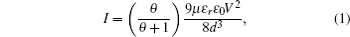
3. Results and discussionFigure 1(a) shows the XRD diffraction pattern for BFO film grown on SRO/STO layers, which exhibits a pure phase of (001)-orientated BFO and an epitaxial structure. When tested at room temperature, they exhibit well-square hysteretic P– V loops with a remanent polarization of 58 μ C/cm2 at a maximum bias voltage (Vm) of 14 V. This is very close to the previously reported value of ∼ 60 μ C/cm2 for high quality BFO single-crystal film.[23] The hysteresis loops also show apparent asymmetric imprint behaviors, which probably originate from the dissimilar electrodes or non-uniform trapped charge distribution adjacent to the metal-oxide interfaces.[14, 15] Typical topological and cross-sectional scanning electron microscopy (SEM) images are shown in Figs. 1(c) and 1(d), respectively. The top view SEM image shows a squarish crystalline structure. From the cross-sectional image, we can clearly identify a sharp double-layer structure with thickness values of ∼ 450 nm and ∼ 60 nm for the BFO and SRO layers, respectively.
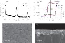
Figure 2 shows the polarization and resistive switching properties at room temperature. During the electrical testing, a bias voltage is applied between the Pt top electrode and SRO bottom electrode, as shown in the inset of Fig. 2(a). At a low maximum bias voltage of 4 V, no I– V hysteresis is observed. The I– V hysteresis loop starts to develop at 6 V, and the loop grows with further increasing Vm. Finally, it stabilizes at Vm of 12 V. It is worth noting that we do not need a power consuming electroforming process to realize the resistive switching, which is usually required in conventional filament-like resistive switching.[16, 24] Figure 2(b) shows the replotted I– V curves in semi-logarithmic scale, which exhibit rather apparent resistive switching at positive bias. In contrast, the resistance variation at negative bias range is rather small, indicating apparent asymmetric resistive behaviors. This is likely to be due to the effects of dissimilar electrodes or non-uniform space charge distribution.[3] We mainly focus on the resistive behaviors at positive bias thereafter. To further study the polarization-modulated resistive switching behavior, we use a sequence of pulsed voltages and subsequently record the small bias resistance/current at 3 V. It is revealed that the read current/resistance as a function of pulsed voltage shows a squarish hysteresis loop, as shown in Fig. 2(c), indicating a typical memristor behavior. It is interesting that the shape of current-pulse voltage curve closely matches with the ferroelectric polarization loop, implying a strong correlation between the resistive switching characteristics and the ferroelectric polarization states. To examine the stability of the resistive switching, we also monitor the retention properties, as shown in Fig. 2(d). We find that the resistance (RL) for the low resistance state (LRS) increases slightly with time rising in logarithmic scale, while the resistance (RH) for high resistance state (HRS) remains rather stable. After 3000 s, the On/Off ratio of RH/RL decreases slightly from 64 to 61. When we extend the time to 10 years by data extrapolation, the ratio still maintains a considerable value of 50, which is large enough for practical data storage application.
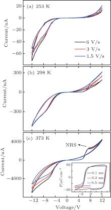
To further understand the conductive mechanisms, temperature dependences of resistive switching characteristics and polarization properties are also investigated. Figure 3 shows the I– V loops in semi-logarithmic scale along with ferroelectric hysteresis loops at different temperatures. The curves are tested by sweeping the bias between ± 12 V, which is considered as being large enough to obtain the saturated resistive switching behavior. We find three distinct characteristics in different temperature ranges, which are listed as follows.
(i) At low temperatures ranging from 173 K to 253 K, the I– V loops are rather small, which seem to be irrelevant to the ferroelectric polarization. Besides, there are two distinct open circuit voltages (OCVs) in both the positive and negative bias ranges. Such OCVs are most probably due to dielectric relaxation-associated charge carriers on both surfaces, which build up open circuit voltages. In addition, we find a hump close to the polarization switching voltage (vanishing at 253 K), which is probably due to the transient displacement current from polarization switching, [22] as will be discussed later. (ii) From 253 K to 298 K, the leakage current increases significantly, while both the OCVs and current hump greatly diminish. These indicate that the great increases in mobility of charge carriers and leakage current[3] have greatly suppressed both the dielectric relaxation-related OCVs and the displacement transient current. With increasing temperature, a resistive switching hysteresis occurs in the I– V curve. At this stage, the resistive switching behaviors can be greatly modulated by the ferroelectric polarization. (iii) From 313 K to 373 K, the low voltage I– V curves are similar to those of stage (ii). Nevertheless, a new resistive switching hysteresis (an abnormal) occurs at a large positive voltage (> 7 V) in addition to the normal ferroelectric resistive switching. The hysteretic behavior becomes more and more apparent with temperature rising. From Fig. 3(b), we can see a well-established squarish polarization hysteresis loop for each individual temperature, indicating that ferroelectric polarization exists in the whole temperature range. It is found that the low temperature I– V hysteresis loops and OCVs do not correlate with the ferroelectric polarization, and the polarization-modulated resistive switching only occurs at relatively high temperatures (above 253 K).
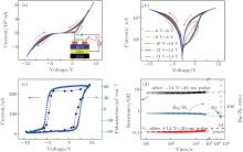
To further understand the conductive mechanisms, we examine carefully I– V and polarization properties at different temperatures. Figure 4(a) shows the I– V loops in linear scale, tested at three different bias sweeping speeds (6 V/s, 3 V/s, 1.5 V/s). It shows a clockwise I– V rotation and a current hump, along with a typical characteristic of OCV for each I– V cure. The OCV voltages decrease as the sweeping speed decreases. To further illustrate the pulsed voltage effect, we use pulsed voltages of ± 14 V to pole the polarization first, and then test the small bias I– V curve (Fig. 4(b)). It is found that the OCV can still be observed at a small value of Vm (3 V) after removing the pulsed voltage. This is very similar to what has been observed by Watanabe in Pb(Ti, Zr)O3/Nb:SrTiO3[25] and (Pb, La)(Ti, Zr)O3/Nb:SrTiO3, [26] and by Saraf et al. in Nd:STO/Fe:STO[27] heterostructures. Such OCVs are often attributed to the so-called dielectric relaxation effect, in which charge carriers can be trapped by both electrodes of the capacitor.[25, 26, 28] The detrapping of carriers can occur in the process of the band bending, leading to the slow release of charge carriers, and consequently to a relaxation time of ∼ 103 s.[26] Saraf et al.[27] has proposed applying the OCV in data storage. However, from our observation, such an OCV possesses very poor retention property, which is not stable enough for application in memory devices.
It is also interesting to see that the current hump becomes increasingly apparent as the voltage sweep speed rises, which most likely originates from ferroelectric displacement current due to polarization reversal.[3, 21, 22] The correlation between the current maximum and polarization switching is further illustrated in Fig. 4(c). Here, we first use two pulsed voltages (± 14 V) to polarize the BFO upwards and downwards, respectively, and then measure the I– V curves. By comparing the I– V curve and saturated P– V curve, it can be seen that the current hump is closely related to the coercive voltage, supporting the result of our previous work that the current maximum is associated with polarization switching.[3, 21, 22] However, it is generally received that the transient displacement current normally occurs on a nanosecond/microsecond time scale at room temperature, [29] which may not be observable on a time scale of milliseconds, as in our case. To verify whether the displacement current is detectable on a time scale of milliseconds at low temperatures, we perform a PUND testing to measure the polarization switching time. Figure 4(d) shows the switched polarization value (Δ P) dependences of pulsed duration at different pulsed voltages. It is found that at a fixed pulsed voltage, Δ P increases with pulsed duration rising, until it reaches the saturated Δ P. The pulse duration required for stabilizing Δ P can be as long as 200 ms at 173 K, which is much slower than that at room temperature. This indicates that the polarization reversal process at low temperature is significantly slower than that at room temperature. Therefore, it is possible to produce the observed current maximum in the I– V curves at around 173 K.
We also measure the I– V behaviors at different bias voltage sweeping speeds for three relative higher temperatures (shown in Figs. 5(a)– 5(c)). At 253 K, both the current humps for displacement current and the OCVs almost vanish, and no resistive switching can be observed in a forward bias range. The current density decreases as the bias sweeping speed rises, which is unlike that at 173 K, exhibiting a normal current relaxation characteristic. As the temperature increases to 298 K, we can see a well-established ferroelectric resistive switching. At a high temperature (373 K) (as seen in Fig. 5(c)), the resistive hysteresis at low voltage is similar to that at 298 K. Nonetheless, there arises a new resistive switching hysteresis in a large bias range (> 7 V). The new resistive switching loop can be explained by the defect-mediated charge trapping/detrapping mechanism.[30] At a higher temperature, more defect-related charge carriers and charge traps can be activated, which may also produce resistive switching through trap filling and unfilling process. From the inset in Fig. 5(c), we can see the distorted polarization loops, which imply that the effects of leakage and charge defects are rather significant. It is suggested that the high trap filling level shifts the quasi-Fermi level and reduces the interface barriers, [14, 30] hence greatly reducing the resistivity and leading to LRS. With a further increase of voltage, some of the trapped charges can be detrapped, resulting in the high resistivity and HRS. It is interesting that the new resistive switching hysteresis starts at around the polarization reversal voltage, indicating that it is likely to be prompted by the polarization reversal. As the ferroelectric polarization bound charge can help to stabilize the trap filling at polarization downward state, once the polarization state switches upwards some of the trapped charges become unstable and will be detrapped at higher voltages. This can also contribute to the formation of the new resistive switching.
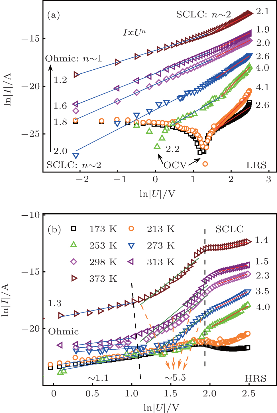
To systematically investigate the conductive mechanisms, we analyze the I– V curves in different temperature and bias ranges. For simplicity, we focus on the positive bias range, in which relatively large resistive switching could be obtained. In ferroelectric oxide films, there may occur some typical conducting mechanisms, including thermionic emission limited (TEL), Poole– Frenkel emission limited (PFL), Fowler– Nordheim tunneling (FNT), and space charge limited (SCLC), and Ohmic behaviors.[14, 15, 29, 31, 32] We replot the I– V curves for both HRS and LRS to fit the individual conducting mechanisms, and find that the I– V behaviors could fit better to the SCLC relation. The SCLC can be described by the following equation[14, 31– 34]
where μ is the electronic mobility, ɛ 0 is the permittivity of free space, ɛ r is the optical dielectric permittivity, V is the bias voltage, d is the film thickness, and θ is a constant related to the charge trap filling status, which is a function of temperature.
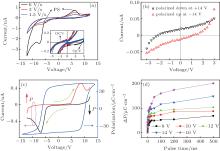
We plot both the LRS (upward polarization) and HRS (downward polarization) I– V curves for different temperatures in Fig. 6. The LRS curves in Fig. 6(a) show well-linear relations as described by I ∝ Vn.[15] At a low temperature (∼ 173 K), the curve deviates from linear relation at low bias, which is likely to be affected by the OCV from dielectric relaxation. At a moderate bias, the curve conforms to the SCLC relation with n ∼ 2. While in a large bias range, n exceeds 2, which may be related to other conducting mechanisms, e.g. FNT, or partially filled deep trap state. As temperature increases from 253 K to 298 K), n varies from 2.2 to 1.8 in a low voltage range (ln V < 1.8), which is nearly consistent with the SCLC relation. For higher voltages (ln V > 1.8), it has a larger n > 2. At high temperatures (313 K and 373 K, Fig. 6(a)), index n gradually reduces to below 1.6 at low bias (ln V < 1.6), which is between SCLC and Ohmic behaviors. This may be related to the partially unfilled trap states, owing to the increase of the number of charge traps activated at elevated temperatures. In this case (> 298 K), the SCLC relation shifts toward higher voltages (ln V > 1.8), which shows a nearly trap-free conductive behavior with n ∼ 2 (1.9– 2.1).
Figure 6(b) shows the I– V curves for the HRS (downward polarization) on a logarithmic scale. The curves fit to the Ohmic and SCLC relations fairy well, similar to those reported by Lee et al.[14] At low temperatures (< 253 K), the curve conforms to the Ohmic conduction (I ∝ V) below bias voltage of ln V ≈ 1.8, suggesting that the shallow traps are not fully filled by charge carriers injected from the electrodes. When the bias voltage increases (to ln V > 1.9), there occurs an abnormal hump at around ferroelectric coercive voltage due to the displacement transient current from polarization reversal, which were discussed previously. At moderate temperatures (253 K– 273 K), the conduction exhibits Ohmic behavior at low bias (ln V < 1.1), beyond which the conduction takes place via a partially deep-trap-filled state, which is reflected with a large slope (I ∝ Vn, n > 3.5) in the graph. At a high temperature (< 298 K), a similar transition of Ohmic conduction to partially deep-trap-filled conduction (n > 2) can be observed below a bias voltage of ln V ≈ 2.1. While at bias voltages (ln V > 2.1), the index n declines to 2.3– 1.4, which indicates that the conduction behavior evolves from deep-trap-filled to partially filled trap states as temperature increases.
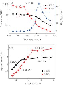
Finally, we also plot the curves of resistance versus temperature, measured at small voltage of 3 V in Fig. 7(a). Both the LRS (downward polarization) and HRS (upward polarization) gradually decrease with the rising of temperature. The On/Off resistance ratio first rises up and then drops down as temperature increases, resulting in a maximum value at around 313 K. It is also worth mentioning that at a low temperature (< 253 K) there is also some extent of resistive-switching-like behavior. However, such a resistive variation is related to the OCV and dielectric relaxation effects, which is not stable. Only above 253 K can we see a robust ferroelectric resistive switching, which is applicable for memory application.
The resistance as a function of 1/T is also plotted in Fig. 7(b). The lnR– (1000/T) curve shows linear relations in different temperature ranges. The behavior well conforms to the Arrhenius relation (R ∝ exp(− Ea/kBT)), where Ea is the activation energy.[29, 35– 37] For the LRS, the activation energy (Ea) deduced from the slope of the linear plot is very small (Ea = 0.04 eV) at low temperatures (< 253 K). Such a small activation energy indicates that the majority of the charge carriers are close to free electrons. From Fig. 6(a), we can see that in similar temperature and bias ranges for the small activation energy, the conduction behaviors are mainly dominated by Ohmic behavior or dielectric relaxation-related OCVs. When the temperature increases above 253 K, the activation energy rises to 0.57 eV, which corresponds to the SCLC conduction region shown in Fig. 6(a). From the SCLC relation in Eq. (1), the constant related to the trap filling state can be written as θ = (Nc /Nt e− (Ec − Et) / kBT, where Nc and Nt are the effective density of states in the conduction band and the density of states for charge traps, and Ec and Et are the electron energies at the minimum of conduction band and energy of trapped charge, respectively; kB is the Boltzmann constant; and, T is the absolute temperature, [33, 34] Therefore, the SCLC conduction also produces an exponential relation against 1/T, and the activation energy derived from the Arrhenius relation can correspond to Ec− Et. Thus, the relatively large activation energy (0.57 eV) at above 253 K for the LRS is most probably attributed to Ec− Et for the SCLC. For HRS (upward polarization), the activation energy is ∼ 0.04 eV below 198 K, which may be also related to electron conduction, above which its activation energy increases to 0.47 eV, and it is likely to be correspondent to Ec− Et for the SCLC. It is also found that there is an apparent variation in activation energy for the SCLCs between the LRS (0.57 eV) and HRS (0.47 eV). The variation of activation energy is associated with the different polarization states, which generate dissimilar bound charge states that are able to attract or repulse charge traps. As a result, we are able to observe an apparent resistive change with a maximum On/Off ratio located at 313 K.
Therefore, at low temperatures (< 253 K) the resistive behaviors in the Pt/BFO/SRO structure are mostly dominated by dielectric relaxation current related to OCVs. At relatively high temperatures (> 253 K), the HRS conducive mechanisms are governed by both the Ohmic conduction in a low voltage range and the charge-trap-related SCLC behavior in a high voltage range. While the LRS is mainly dominated by the SCLC conduction. The polarization reversal is able to change the low voltage conductive behavior from Ohmic conduction to SCLC. This causes a significant variation in resistivity, which is likely to be due to the change of trap filled status which can be affected by the polarization bound charge-related interface energy band bending. At high temperatures (> 298 K), an additional resistive switching appears in a high bias voltage range. This is likely to be related to the defect-mediated trapping/detrapping effects. Our observations indicate that in a high quality BFO film, the general ferroelectric resistive switching is more likely to originate from the polarization-modulated SCLC conduction, rather than from the defect-mediated trapping/detrapping process. In highly defective films, other conduction mechanisms like trapping/detrapping process can also occur. Our work may help to clarify some of previous controversies regarding the ferroelectric resistive switching mechanism.
However, since SCLC is a bulk effect, it is unlikely to produce the observed asymmetric conductive behaviors between the forward and backward I– V curves. This discrepancy can be accounted for by the existence of a defective layer (e.g. oxygen vacancy layer) adjacent to Pt/BFO interface, which could be produced in a film deposition process and which acts as charge carrier traps for the SCLC behavior.[14] Therefore, it is critical to control the defect layer to improve the resistive switching properties for certain applications.


 , Yan Zhi-Bo