


Effects of surface adsorbed oxygen, applied voltage, and temperature on UV photoresponse of ZnO nanorods
[Zong Xian-Li, Zhu Rong† ]
]
]
|
|


†Corresponding author. E-mail: rong zhu@263.net
*Project supported by the National Natural Science Foundation of China (Grant No. 91123017).
The ultraviolet (UV) photoresponses of ZnO nanorods directly grown on and between two micro Au-electrodes by using electric-field-assisted wet chemical method are measured comprehensively under different conditions, including ambient environment, applied bias voltage, gate voltage and temperature. Experimental results indicate that the photoresponses of the ZnO nanorods can be modulated by surface oxygen adsorptions, applied voltages, as well as temperatures. A model taking into account both surface adsorbed oxygen and electron-hole activities inside ZnO nanorods is proposed. The enhancement effect of the bias voltage on photoresponse is also analyzed. Experimental results shows that the UV response time (to 63%) of ZnO nanorods in air and at 59 °C could be shortened from 34.8 s to 0.24 s with a bias of 4 V applied between anode and cathode.
One-dimensional ZnO nanorods (NRs) and nanowires (NWs) have a wide band gap energy of 3.3 eV, high electron binding energy of 60 meV, high electron mobility, and large piezoelectric coefficient.[1] Therefore, they have attracted a lot of attention as promising materials with broad applications in piezoelectric nanogenerators, [2] UV sensors, [3] light-emitting diodes, [4] etc. In the study of UV sensors, a majority of ZnO films[4, 5] and nanostructures[6– 11] exhibit a slow photoresponse, which was usually supposed to be attributed to the slow surface adsorption and desorption processes of oxygen molecules.[6– 10] In practical applications, the response time of a sensor is a critical performance index. The slow response of ZnO nanomaterial will seriously hinder its applications in UV photosensitive sensors. So improving the photoresponse time of ZnO nanorods is of great importance.
In this paper, a three-electrode FET structure including two top electrodes (anode and cathode) and gate electrode is presented. Growth of ZnO nanorods (ZnO NRs) on and between anode and cathode is achieved by using the electric-field-assisted wet chemical method. Photoresponse measurements under different bias voltages between anode and cathode are carried out in air, vacuum and under different oxygen pressure, respectively. A model taking into account surface adsorbed oxygen and electron-hole activities inside ZnO nanorods is proposed. In order to verify the mechanism, UV illumination measurements of ZnO nanorods before and after coating parylene C are also conducted. The influence of gate potential and temperature on the photoresponse of nanorods are further tested and analyzed. Experimental results indicate that: surface oxygen adsorption and desorption could shorten the UV response time but reduce the photocurrent; increasing bias voltage between anode and cathode could enhance the photocurrent and speed up the UV response; and, the UV response time of ZnO nanorods can be significantly shortened by increasing the temperature.
The ZnO nanorod UV detector was fabricated by using a wet chemical method, with alternating current (AC) electric-field applied to three-electrode microstructure, [12, 13] as shown in Fig. 1. A similar field effect transistor (FET) structure with three electrodes including two top coplanar electrodes (anode and cathode) and a bottom electrode (gate) was used to grow ZnO nanorods on micro electrodes directly. The fabrication process started with thermal oxidation of a 0.008-Ω · cm∼ 0.02-Ω · cm N-doped silicon wafer (served as gate) to form the 500-nm insulation layer. Next, the SiO2 layer was masked and etched to expose the gate electrode. Afterwards, 100-nm Cr/Au film was deposited on the SiO2 layer and patterned by photolithography to form a comb-like anode and cathode with a gap distance of 4 μ m. Wire bonding was used to connect three electrodes with outside pins. Then, the chip was immerged in equal molar aqueous solution (0.015 M) of Zn(NO3)2 and HMTA at 75 ° C. A sine wave AC power (1 MHz, 3.5 Vpp∼ 4.5 Vpp) was applied to anode and cathode while the gate was connected to a DC power (0 ∼ − 40 mV). After 3.5 h, the chip was picked up from the solution, rinsed with deionized water, and dried in air.
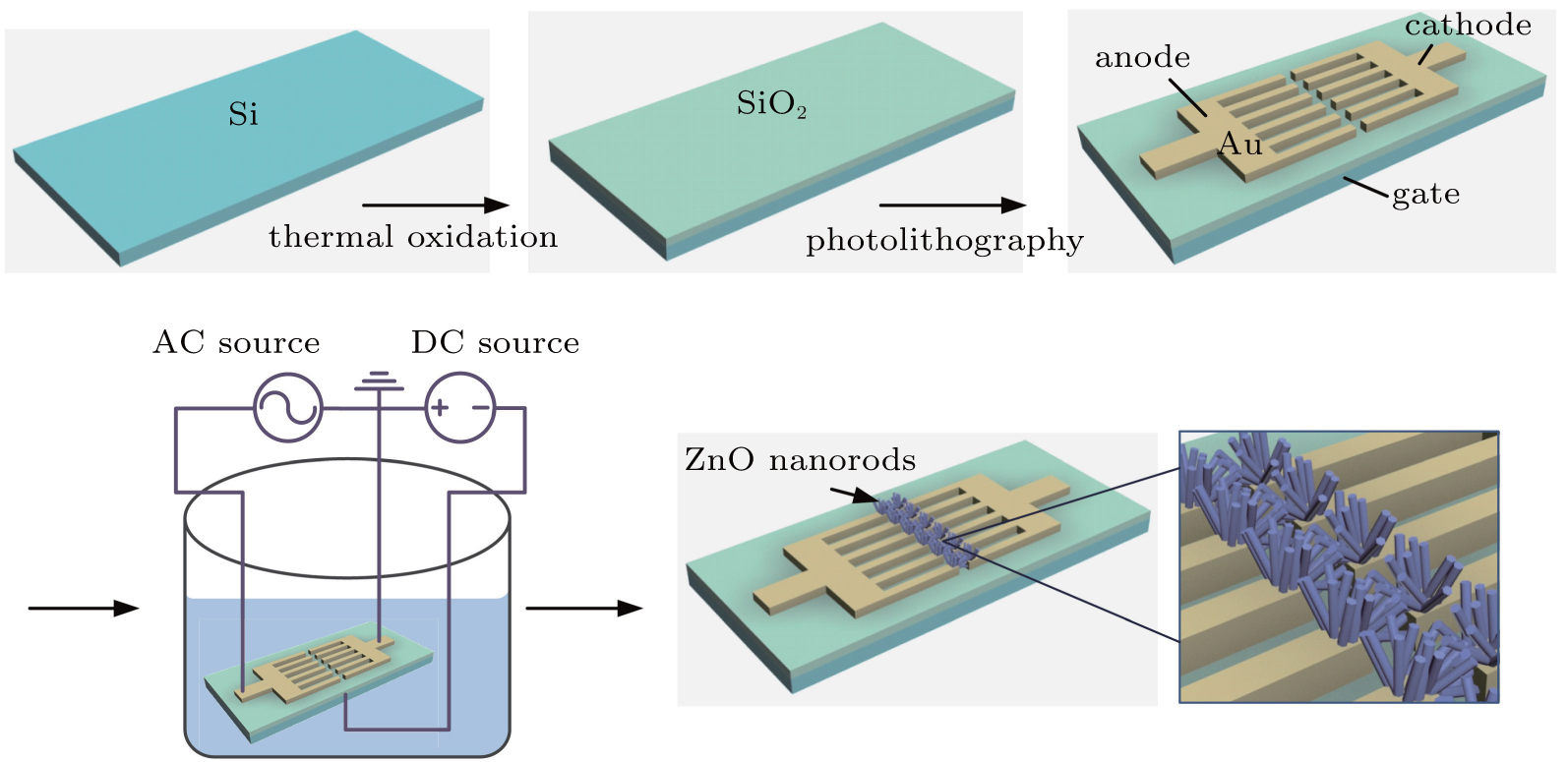 | Fig. 1. Schematic illustration of the set-up for growing ZnO nanorods on and between electrodes. |
The UV measurements were conducted under the illumination of a 365-nm UV light emitting diode (LED) (Ocean Optics, LLS) with a 10-nm FWHM (full width at half maximum) and intensity of 1.26 mW under 13% RH at room temperature of 23.5 ° C. The UV light was transmitted and guided by fibers to irradiate the chip with ZnO NRs. The currents through nanorods were measured using a sub-femtoamp meter (Keithley 6430). The temperature control was performed by using a temperature controlled oven (CIMO DZF-6020).
Four ZnO NRs samples (1, 2, 3, and 4) were used to carry out the measurements under different conditions. Samples 1, 2, and 3 were used to investigate the influence of the ambient atmosphere and applied bias voltage on the UV photoresponse of ZnO nanorods. Sample 4 was used to investigate the influence of the gate voltages and temperature.
Figure 2 shows the scanning electron microscopy (SEM) images of single crystalline ZnO nanorods growing on and between the anode and cathode. Figures 2(b) and 2(c) show higher resolution SEM images of Fig. 2(a), indicating an average diameter of 300 nm– 500 nm and an average length of 3 μ m∼ 5 μ m of ZnO NRs.
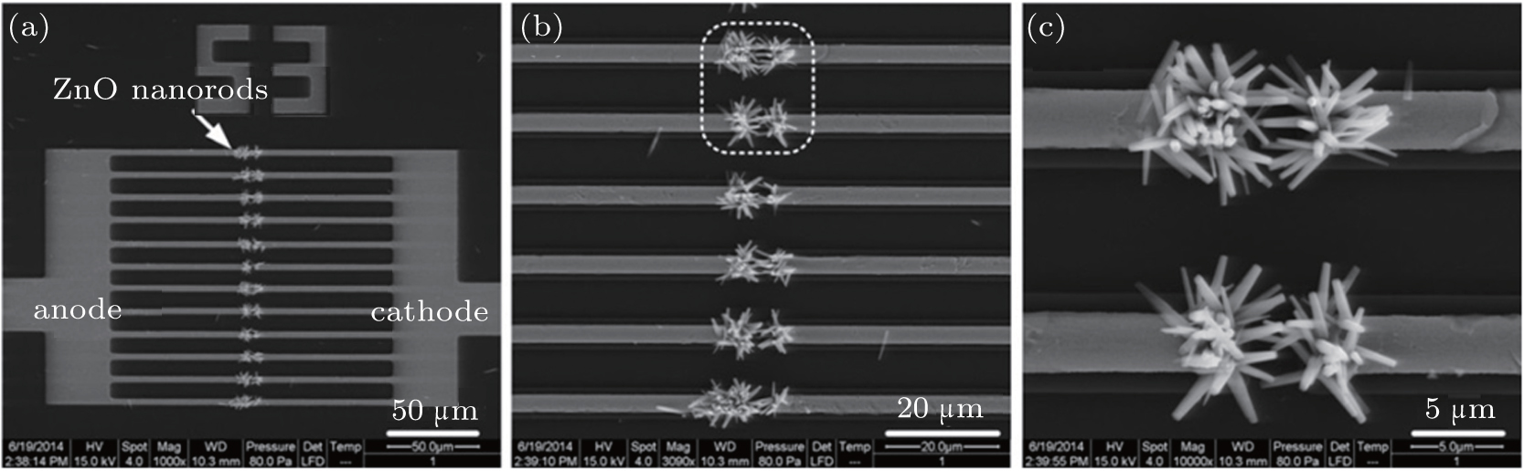 | Fig. 2. SEM images of ZnO nanorods growing on and between the microelectrodes. Panels (b) and (c) show the higher resolution SEM images of panel (a). |
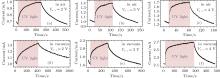
Sample 1 is used to investigate the time-resolved photocurrent rise and decay of ZnO nanorods by switching on and off the UV LED in air and vacuum (4 Pa∼ 6 Pa), as shown in Fig. 3. From left to right, the curves are obtained with bias voltages of 2, 3, and 4 V, respectively. Dark current, saturation current under UV illumination, photocurrent (difference between the saturation current under UV illumination and the dark current), rise time (to 63%) and decay time (to 37%) under different conditions are summarized in Table 1. The results in Table 1 exhibit that when changing the ambient environment from air into vacuum, the dark current and photocurrent both become larger and the UV response turns slower. Specifically, with ambient environment changing from air to vacuum for sample 1 at a bias voltage of 4 V, the dark current increases from 1.23 mA to 2.13 mA and the photocurrent slightly increases from 0.47 mA to 0.58 mA. In addition, the rise time increases from 3.2 s to 9.1 s and the decay time increases from 24.4 s to 54.6 s. These results indicate that the air environment can speed up the UV response, which is consistent with most of the relevant literature reports.[4, 5]
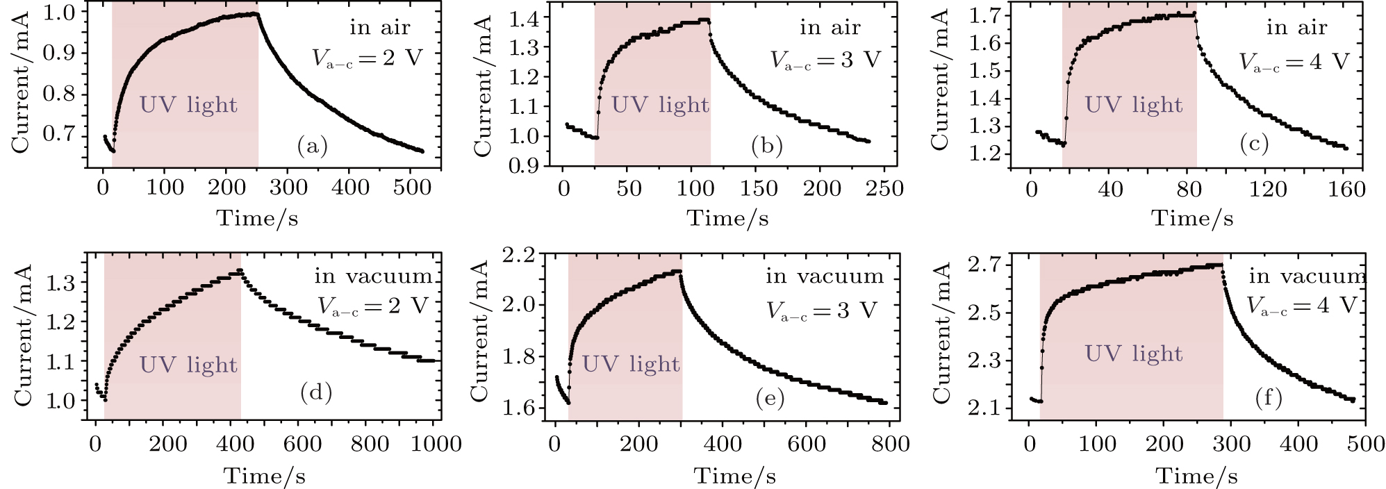 | Fig. 3. Time-resolved photocurrent rise and decay of ZnO nanorods sample 1 in air ((a)– (c)) and vacuum (4 Pa∼ 6 Pa) ((d)– (f)) at bias voltages between anode and cathode (Va − c) of 2, 3, 4 V (from left to right, respectively. All the measurements are conducted under the illumination of a 365-nm UV LED with an intensity of 1.26 mW at 23.5 ° C under 13% RH. |
| Table 1. Illumination results with different ambient conditions and bias voltages. |
In other reports, the slow response of ZnO UV detector exposed in a low pressure or vacuum is usually attributed to the lower density of oxygen, which results in slower equilibrium processes of oxygen adsorption and desorption on the surface of ZnO nanostructures.[
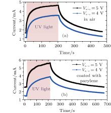
 | Fig. 4. Time-resolved photocurrent rises and decays of ZnO nanorod sample 2 (a) in air and (b) after coating with parylene C with different bias voltages between anode and cathode (Va − c). |
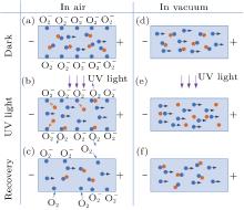
To explain these phenomena, a model taking into account surface adsorption and desorption together with electron-hole activities inside ZnO nanorods is proposed. The mechanisms of the photoresponse in air and vacuum are summarized in Fig. 5. In an n-type semiconductor, the electrons play a main role in making the contribution to conductivity, so the effect of holes on conductivity can be ignored. In the dark air environment (Fig. 5(a)), oxygen molecules are adsorbed on the surface by trapping free electrons 

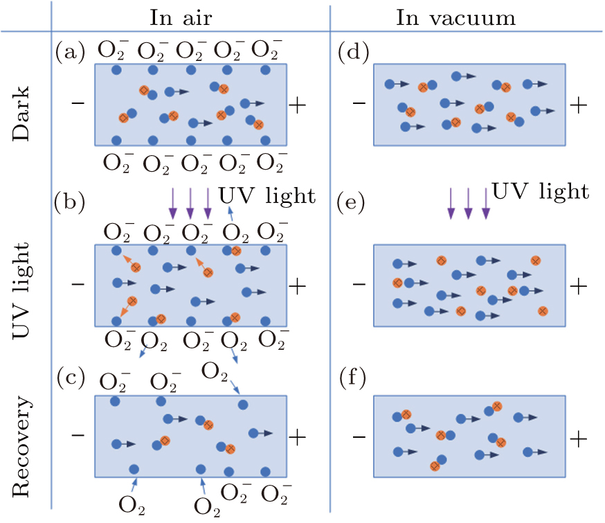 | Fig. 5. Schematic views of the UV photoresponse process of a ZnO nanorods in air ((a)– (c)) and vacuum ((e)– (g)). Blue and orange grid solid dots represent electrons and holes, respectively. |
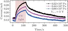
Further, UV photoresponse measurements are conducted under different oxygen partial pressures (0.22× 10⁵ Pa, 0.44× 10⁵ Pa, and 0.88× 10⁵ Pa) by increasing the chamber pressure using an air compressor. The results are shown in Fig. 6 and Table 2. These results show that with the increase of oxygen partial pressure, more electrons are trapped by oxygen molecules, thus creating a deeper surface depletion layer. Therefore, the UV photoresponse is accelerated and the photocurrent is reduced.
 | Fig. 6. UV photoresponses with different oxygen partial pressures (2.2× 10⁴ Pa, 4.4× 10⁴ Pa, and 8.8× 10⁴ Pa) at the same applied voltage between anode and cathode (Va − c = 3 V). |
| Table 2. Illumination results with different oxygen partial pressures at an applied voltage of 3 V. |
In the above experiments, we found that the increasing of bias voltage between anode and cathode could help to enhance the photocurrent and speed up the UV response. Specifically, when the bias voltage rose from 2 V to 4 V for sample 1 in air, the dark current increased from 0.67 mA to 1.23 mA and the photocurrent increased from 0.32 mA to 0.47 mA as the rise time shortened from 42 s to 3.2 s and the decay time shortened from 96.7 s to 24.4 s. According to semiconductor physics theory, [

where τ n and τ p are photo-generated excess carrier lifetimes for electrons and holes, respectively, tn and tp are transit times for electrons and holes, respectively, μ n and μ p are the electron and hole mobilities, V is the applied voltage, and L is the separation between two electrodes. Equation (1) shows that with the increase of V, the photoconductive gain G is increased, which means the photocurrent will be enhanced. According to the reports, [10, 16] the deep defect states in ZnO NRs can bring a long carrier relaxation process and make the photoresponse slow. When increasing the applied voltage, the carriers have a higher energy to escape from the trap states, which results in the shortening of the relaxation time, and this accelerates the photocurrent response.
Based on the above analysis, the potential gradient across nanorods, created by surface oxygen adsorption, can trap excess holes and reduce the probability of combination between electrons and holes in the illumination process, thus accelerating the UV response. To further validate the potential gradient effect, we generate additional potential gradients across nanorods by applying different bias voltages (− 15 V, − 10 V, and 10 V respectively) to the bottom gate and applying the same bias voltage (4 V) between anode and cathode. The photoresponse measurements are shown in Figs. 7(a) and 7(b). The results summarized in Table 3 illustrate that by applying the gate voltages, dark currents increase almost twice higher than that with null voltage. That probably happens because a monotonic outside additional potential gradient will be created, with a gate voltage applied. Under this condition, the adsorption of oxygen molecules can only be conducted on one side of ZnO nanorods surface. So less free electrons will be trapped, which induces both dark current and photocurrent to increase. Upon UV illumination, excess electrons and holes are generated. In addition to migrating to the one side-surface to release 
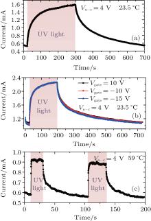
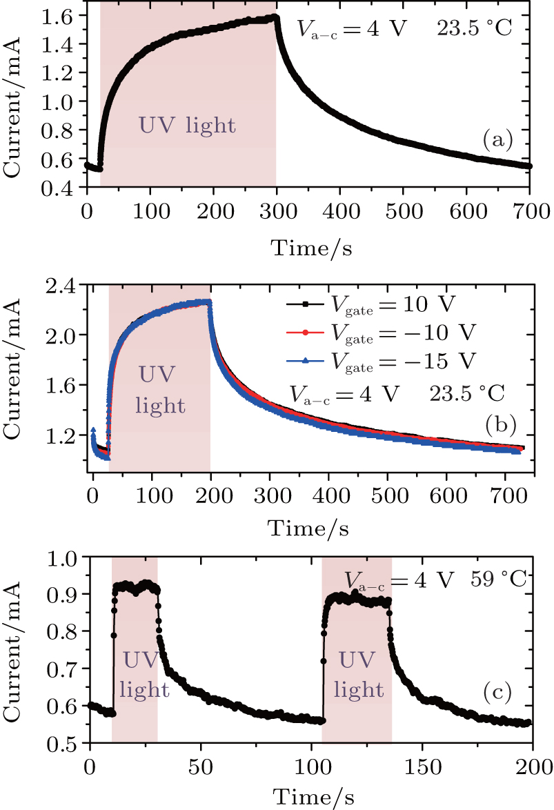 | Fig. 7. Time-resolved photocurrent rises and decays of ZnO nanorods sample 3 in air with gate voltage (Vgate) values of 0 V (a), and 10 V, − 10 V, − 15 V (b) with the same bias voltage of 4 V between anode and cathode (Va − c). Temperatures are 23.5 ° C ((a) and (b)) and 59 ° C (c). |
| Table 3. Illumination results of sample 4 with different temperatures and gate voltages, with the applied voltage between anode and cathode being 4 V. |
A UV response experiment by using sample 3 in air at a higher temperature of 59 ° C is also conducted, as shown in Fig. 7(c) and the results are also summarized in Table 3. By increasing the temperature from 23.5 ° C to 59 ° C, the rise time and decay time of UV response significantly shorten from 34.8 s to 0.24 s and from 90.9 s to 7.1 s, respectively. The accelerating reason is that ZnO NRs grow from anode and cathode simultaneously and meet in the middle of the cathode-anode gap, forming the bascule-bridge contacts and influencing the UV photoresponse of ZnO NRs according to the reports in Ref. [
In this paper, the UV photoresponse of ZnO nanorods that are directly grown on and between micro-electrodes by using electric-field-assisted wet chemical method are measured comprehensively in air, vacuum, under different applied voltages, and at different temperatures. A model illustrating the mechanisms of surface adsorption effect and electron-hole activities inside ZnO nanorods in UV response process is proposed and experimentally validated. Our experimental results show that the surface adsorbed oxygen and raising temperature can help to shorten the UV response time but reduce the photocurrent of ZnO nanorods, while increasing the bias voltage between anode and cathode will enhance both the photocurrent and the response speed. By exposing ZnO nanorods to air at 59 ° C, and by applying a bias voltage of 4 V between anode and cathode, a shorter rise time (to 63%) from 34.8 s to 0.24 s is reached for our UV detector.
| 1 |
|
| 2 |
|
| 3 |
|
| 4 |
|
| 5 |
|
| 6 |
|
| 7 |
|
| 8 |
|
| 9 |
|
| 10 |
|
| 11 |
|
| 12 |
|
| 13 |
|
| 14 |
|
| 15 |
|
| 16 |
|
| 17 |
|