Structural and optical characteristic features of RF sputtered CdS/ZnO thin films
Al-Baradi Ateyyah M1, †, Altowairqi Fatimah A1, Atta A A1, 2, Badawi Ali1, Algarni Saud A1, Almalki Abdulraheem S A3, Hassanien A M4, Alodhayb A5, Kamal A M6, El-Nahass M M2
Department of Physics, Faculty of Science, Taif University, Taif 21974, Saudi Arabia
Department of Physics, Faculty of Education, Ain Shams University, Roxy 11757, Cairo, Egypt
Department of Chemistry, Faculty of Science, Taif University, Taif, Saudi Arabia
Department of Physics, College of Science and Humanities – Al Quwaiiyah, Shaqra University, Saudi Arabia
Research Chair for Tribology, Surface, and Interface Sciences, Department of Physics and Astronomy, College of Science, King Saud University, Riyadh 11451, Saudi Arabia
Department of Physics and Astronomy, College of Science, King Saud University, Riyadh 11451, Saudi Arabia


† Corresponding author. E-mail: thobyani@yahoo.com

Project supported by the Deanship of Scientific Research, Taif University, Kingdom of Saudi Arabia (Grant No. 1-440-6136).

Abstract

In this study, CdS/ZnO (2:3 mol%) thin films are successfully deposited on quartz substrates by using the sputtering technique. Good images on the structural and optical characteristic features of CdS/ZnO thin films before and after annealing are obtained. The CdS/ZnO thin films are annealed respectively at temperatures of 373 K, 473 K, and 573 K and the structural features are examined by XRD, ATR-FTIR, and FESEM. The optical properties of CdS/ZnO thin films such as refractive indices, absorption coefficients, optical band gap energy values, Urbach energy values, lattice dielectric constants, and high frequency dielectric constants are determined from spectrophotometer data recorded over the spectral range of 300 nm–2500 nm. Dispersion parameters are investigated by using a single-oscillator model. Photoluminescence spectra of CdS/ZnO thin films show an overall decrease in their intensity peaks after annealing. The third-order nonlinear optical parameter, and nonlinear refractive index are also estimated.

PACS: ;07.79.-v;;73.61.-r;
1. Introduction

In recent years, the binary nanocomposites materials have received much attention of scientists due to their distinguished performances in microelectronic, optoelectronic devices, photocatalysts, and optics. Binary nanocomposites such as cadmium sulphide–zinc oxide (CdS/ZnO) shows good stable transport properties and has many interesting applications in optoelectronic devices.[17] Coupling of CdS/ZnO nanostructures has been continuously attractive and produced innovative prospects for numerous modern optoelectronic devices. Thin films consisting of (CdS/ZnO) nanocomposites have been widely explored due to their applications in the area of optoelectronic, photo-catalysis and optics.[812]

The CdS possesses a narrow direct optical band gap (∼ 2.4 eV) and is extensively used as a visible light photocatalyst. The CdS is the most appropriate visible sensitizer for zinc oxide (ZnO) because its crystal lattice constant is similar to that of ZnO, having the optical band-gap energy in the visible light region creating a heterojunction with zinc oxide, which enables a very fast interband electronic charge transfer between these compounds. The electronic charge injection from ZnO to CdS produces an efficient electronic charge separation due to a decrease in the exciton recombination; one of the excitons is bounded to the ZnO and the other to the coupled CdS.[13,14] The CdS is suitable to constructing the core-shell heterostructures with ZnO, including one-dimensional core–shell heterostructure, which are the most promising heterostructures for photo-catalytic and solar energy applications.[1521] In the CdS/ZnO nanostructures, ZnO is a wide optical band gap in the range of ∼ 3.34 eV. It is responsible for a charge separation that suppresses the recombination process.[22] The CdS/ZnO nanostructures also have better physicochemical characteristics than the constituents. For example, the conductivity of CdS/ZnO nanostructure is better than that of pure ZnO nanorod.[23,24]

Structural and optical characteristic features of nanostructured CdS/ZnO thin films have been previously investigated by many researchers.[2528] They reported that the optical properties and the optical band gaps of the nanostructured CdS/ZnO thin films can be controlled by the content ratio.

In the present study, we focus our attention on the influence of the annealing temperature on microstructural (FTIR, XRD, EDX and FESEM), optical, and photoluminescence properties of binary nanocomposites materials (CdS/ZnO) thin films.

2. Methods and materials

The CdS/ZnO thin films were deposited on quartz substrates by using the UNIVEX 350 sputtering coating technique. The deposition parameters of CdS/ZnO thin films are listed in Table 1.

Table 1.

Experimental parameters of sputtering-deposited CdS/ZnO thin films.

.

The chemical bonds of the CdS/ZnO thin films were estimated using attenuated total reflection Fourier transform infrared (ATR-FTIR) spectrometer (Bruker, Germany) with using reflection mode. The attenuated total reflection Fourier transform infrared (ATR-FTIR) spectra of the CdS/ZnO thin films were obtained in the spectral range from 4000 cm−1 to 450 cm−1. FESEM analysis of transparent CdS/ZnO thin films was done using SEM Model Quanta 250 field emission gun, FEI Company, Netherlands. The crystalline structures of CdS/ZnO thin films were examined by x-ray diffraction (XRD) using a D8 Advance (Bruker, USA) x-ray diffractometer with Cu (λ = 1.54056 Å) operated at 40 kV and 40 mA. The scanning angular range was from 7° to 90° in 2θ.

The optical data (transmittance and reflectance) were taken by using a V-670 JASCO spectrophotometer that covers wavelengths of 300 nm–2500 nm. The V-670 JASCO spectrophotometer was connected with a constant angle specular reflection accessory (5°). The optical quantities n (real part of the refractive index) and k (extinction coefficient) of the CdS/ZnO thin films are calculated using the same methods as that reported in Refs. [2932].

As reported in Ref. [33], the experimental errors in measuring the film thickness and the T (or R) parameter were estimated at ±2% and ± 1%, respectively; whereas, the errors in measuring n and k were less than ±4%. A JASCO (FP-8200A) specrofluorometer with λexcitation = 300 nm was used to investigate the emission spectra of the as-deposited and thermally annealed CdS/ZnO thin films.

3. Results and discussion

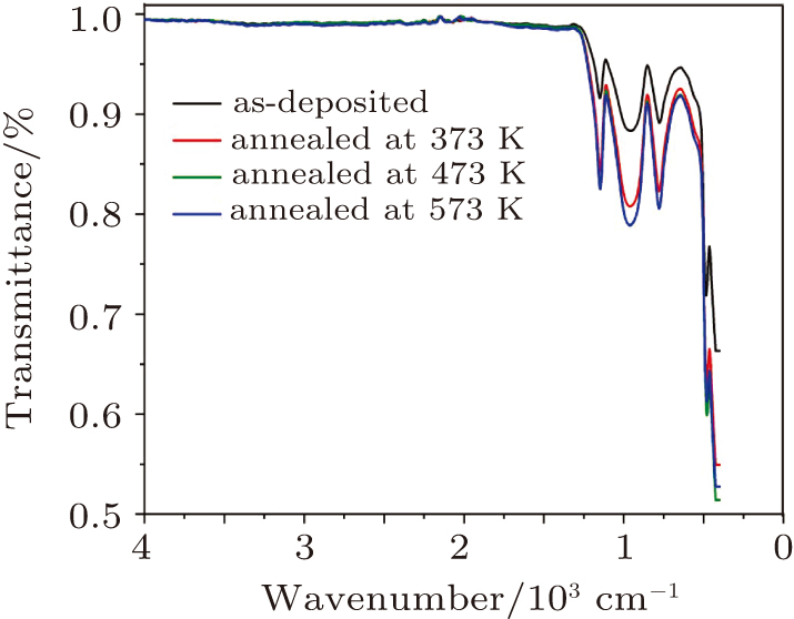
The FT-IR spectra of CdS-ZnO for the as-deposited and thermally annealed CdS/ZnO thin films are shown in Fig. 1 within the range of 450 cm−1 to 4000 cm−1. In the higher energy region, there are not any detectable peaks due to O–H stretching of absorbed water vapor on the surface of CdS–ZnO thin films. The band positioned at 485 cm−1 is attributed to Zn–O zinc oxide bond, which confirms the formation of ZnO.[34] There are two bands at 960 cm−1 and 775 cm−1 due to the stretching frequency of Cd–S bond.[35] The band at 1150 cm−1 corresponds to the S–O stretching vibration of the CdS–ZnO thin film.[36]

Fig. 1. FTIR spectra of as-deposited and thermally annealed CdS/ZnO thin films.

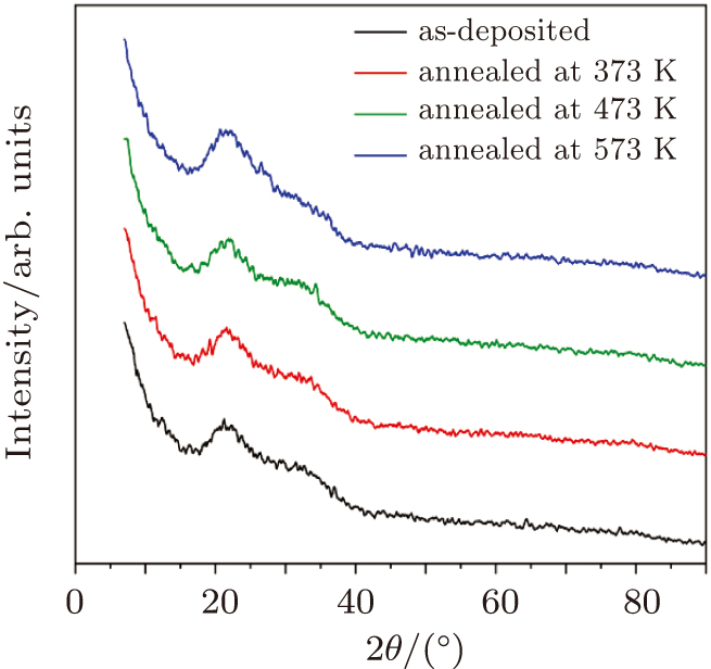
Figure 2 shows the observed XRD patterns for the as-deposited and thermally annealed CdS/ZnO thin films. It can be seen that the as-deposited and annealed CdS/ZnO thin films display no remarkable recognizable reflection of either ZnO or CdS; the films each have an amorphous structure (lack of clear diffraction peaks) and at these annealing temperatures are not adequate to form a crystalline phase for each of CdS/ZnO thin films.

Fig. 2. Observed XRD patterns of as-deposited and thermally annealed CdS/ZnO thin films.

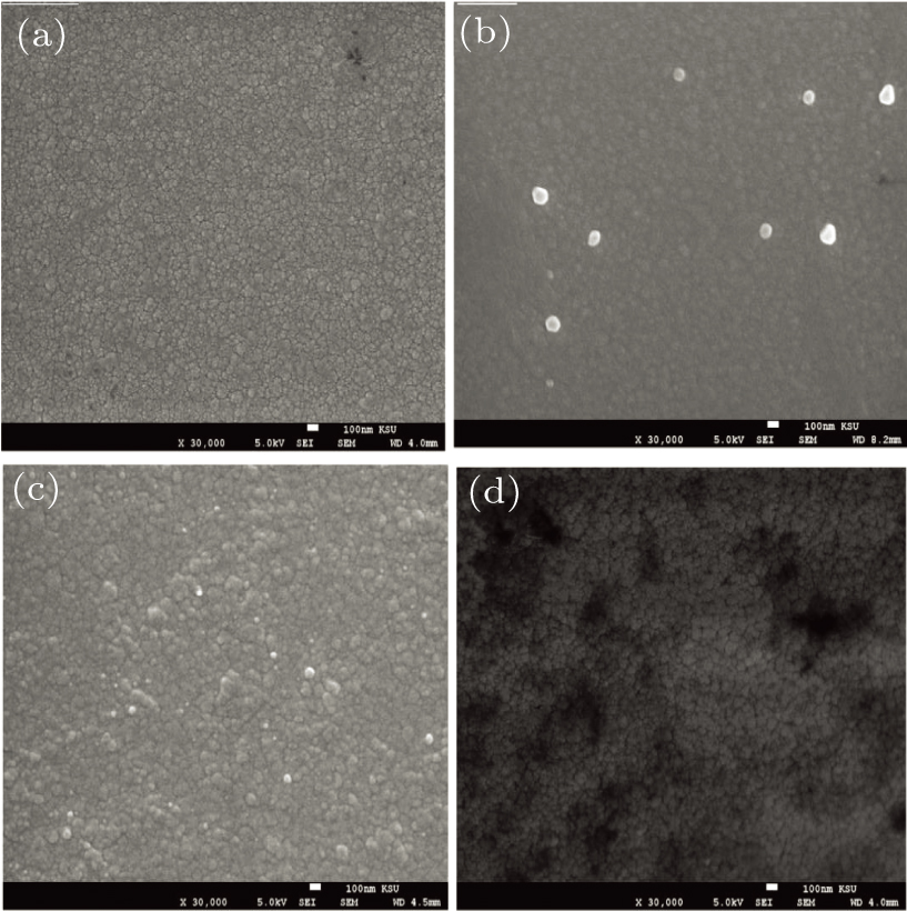
Figure 3 shows the FESEM micrographs of the as-deposited and thermally annealed CdS/ZnO thin films. The as-deposited and annealed CdS/ZnO thin films show low roughness with no vacancy and uniform distribution with small agglomeration (homogeneity) across the scanned areas and no cracks were observed on their surfaces. The FESEM micrographs reveals that the quartz substrate is well covered by a large number of sphere-like structures with different diameters. The observed mean size of the as-deposited and annealed CdS/ZnO particles is in a range of 120 ± 9 nm.

Fig. 3. FESEM micrographs of as-deposited and thermally annealed CdS/ZnO thin films as a function of temperatures: (a) as-deposited film, (b) annealed film at 373 K, (c) annealed film at 473 K, and (d) annealed film at 573 K.

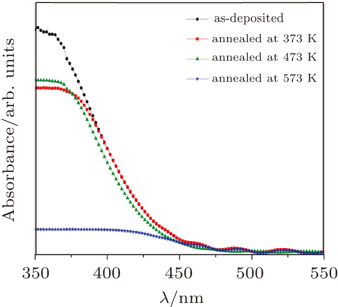
The absorbance spectra of the as-deposited and thermally annealed CdS/ZnO thin films are presented in Fig. 4. The CdS/ZnO thin films show better absorbance in the wavelength range of 350 nm–400 nm and lower absorbance in the wavelength range of 450 nm–550 nm. One can see that the improvement of the optical absorbance (decrease in absorbance) of the thermally annealed CdS/ZnO thin films results from the increase in the transparency of the films.

Fig. 4. The absorbance spectra of as-deposited and thermally annealed CdS/ZnO thin films.

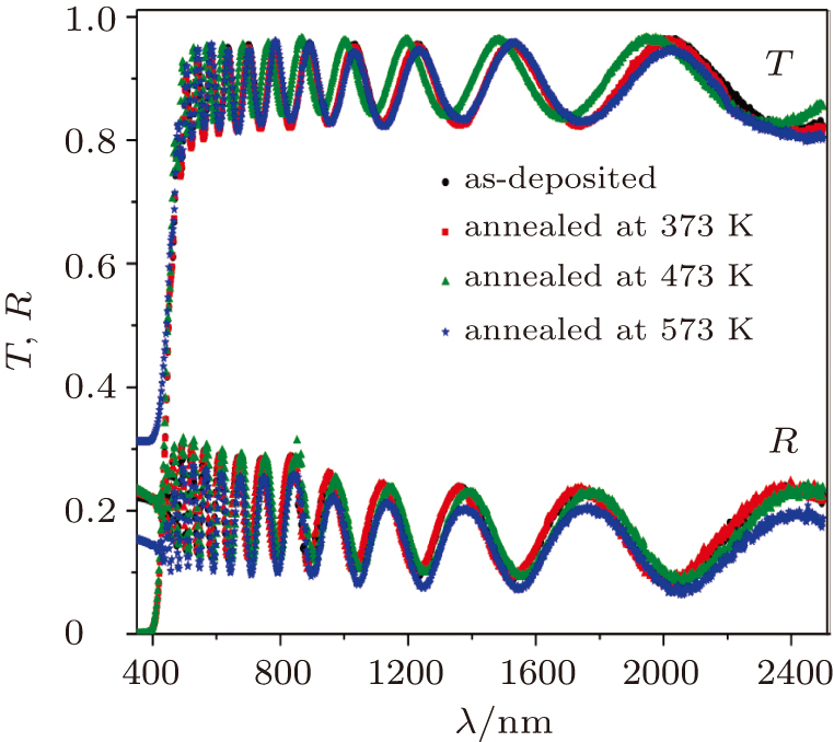
Figure 5 shows the spectrophotometrically measured curves of R and T versus the wavelength for the as-deposited and thermally annealed CdS/ZnO thin films. The well oscillating and homogenous interference fringes of the optical transmissions indicate that the as-deposited and thermally annealed CdS/ZnO have flat surfaces and the film thickness has a uniform distribution.[37] The distinct absorption band edges are at λ ≈ 400 nm, and these band edges of the as-deposited and thermally annealed CdS/ZnO are not strongly affected by the annealing temperature up to 573 K. The presence of such a sharp band edge in the visible region indicates that the CdS/ZnO thin films each possess a good band pass at λ > 400 nm. The as-deposited and thermally annealed CdS/ZnO thin films display no significant difference in their reflectance spectrum patterns.

Fig. 5. Transmittance and reflectance spectra of asdeposited and thermally annealed CdS/ZnO thin films.

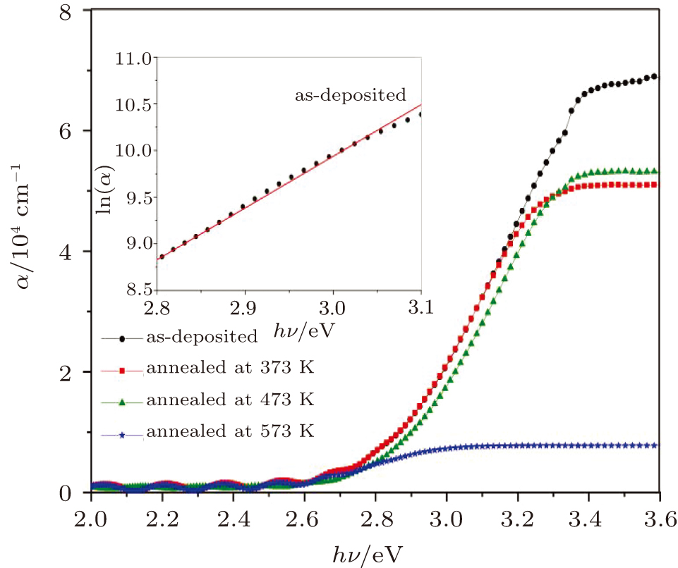
The variations of absorption coefficient α with wavelength (where α = 4πk/λ) for the as-deposited and thermally annealed CdS/ZnO thin films are shown in Fig. 6. The wavelength-dependent absorption coefficients show two sections: an exponential region at lower energy and a power law region at high photon energy.

Fig. 6. Spectral dependence of absorption coefficient of as-deposited and thermally annealed CdS/ZnO thin films with inset showing energy dependence of ln(α) for as-deposited and thermally annealed CdS/ZnO.

In the lower energy region, where the absorption coefficients vary exponentially with , the exponential dependence of the absorption at the band edge is due to the perturbation of the density of the states (DOS). The spectral dependence of the absorption edge follows the Urbach energy (Eu), which describes the width of the absorption tail as given in the following expression:[38]

The plot of ln(α) versus hν for the as-deposited and thermally annealed CdS/ZnO film is displayed in the inset of Fig. 6. The calculated values of Eu for the as-deposited and thermally annealed CdS/ZnO are given in Table 2. These results support that the optical band gap widening CdS/ZnO thin films can be due to the decrease of the band tail, while the decrease of optical band gap could be attributed to the widening of the band tail.

Table 2.

Optical parameters of transparent CdS/ZnO thin films.

.

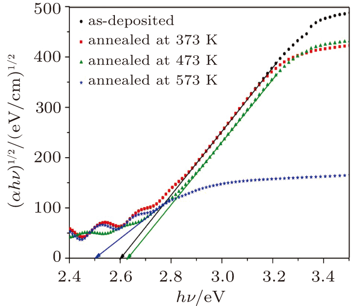
The optical band gap energy values of the as-deposited and thermally annealed CdS/ZnO thin films and the type of optical electronic transitions are assessed from the examination of the absorption coefficient, α, versus hν nearby the fundamental absorption edge by using the allowed indirect transitions expression:[39]

where is the allowed indirect optical band gap energy, Aind is the characteristic transition parameter, independent of photon energy, and Ephanton is the phonon assisted transitions. As observed in Fig. 7, the values of indirect allowed optical band gap of the as-deposited and thermally annealed CdS/ZnO thin films are calculated by extrapolating the linear section of the plot (αhν)1/2 as a function of () and taking the intercept on the () axis. The calculated values of optical band gap are given in Table 2. The optical band gap displayed a blue shift with temperature increasing up to 473 K. The band bending effect (temperatures band will become sharper, and the gap will be wider) gives an acceptable explanation to this phenomenon.[40,41] Slight red shift in the band gap at 573 K can be discussed based on band gap narrowing effect through many-body effects like electron–electron and electron–ion scatterings.[42]

Fig. 7. Plots of (αhν)1/2 versus hν for as-deposited and thermally annealed CdS/ZnO thin films.

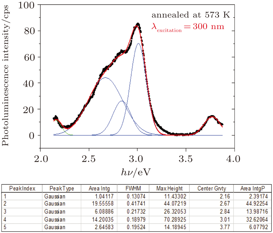
Photoluminescence emission is a key mechanism in the study of light emission properties of optoelectronic semiconductor devices, optical communication and lasers.[43] Photoluminescence emission at room temperature is performed for the as-deposited and thermally annealed CdS/ZnO thin films with λexcitation = 300 nm. The photoluminescence emission spectra are shown in Fig. 8. The photoluminescence spectra of the CdS/ZnO thin films show an overall decrease in their peak intensities after annealing. These figures, i.e., Figs. 8(a)8(d), show emission peaks centered at 330 nm, 410 nm, 426 nm, 461 nm, and 573 nm, respectively. A Gaussian fitting to the emission spectrum of the annealed CdS/ZnO thin film at 573 K is shown in Fig. 9. With the constant background subtracted, the emission spectra are deconvoluted into different components, followed by a Gaussian fitting. The emission peaks are attributed to the intrinsic defects such as sulfur vacancies, surface states, and oxygen vacancies.[44] The maximum in the photoluminescence emission is “Stokes shifted” with respect to the absorption edge in the CdS/ZnO thin film due to capturing the defect states and trapping.[43]

Fig. 8. Room-temperature PL spectra of as-deposited and thermally annealed CdS/ZnO thin films excited at 300 nm.
Fig. 9. De-convoluted analysis of annealed CdS/ZnO thin film at 573 K.

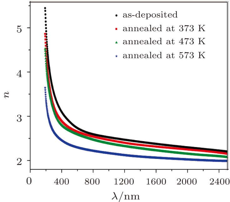
Figure 10 shows the variations of refractive index (n) with wavelength for the as-deposited and thermally annealed CdS/ZnO thin films. In this figure, each curve displays that the value of n sharply decreases with λ increasing in the range of λ < 500 nm and slightly decreases in the range of λ > 500 nm. The values of the refractive index slightly decrease by annealing up to 573 K with respect to the as-deposited CdS/ZnO film. This decrease in the refractive index may be attributed to the improvement in stoichiometry of the films due to the reaction of oxygen.

Fig. 10. Spectral dependence of mean real part of refractive index, n, of as-deposited and thermally annealed CdS/ZnO thin films.

At the low optical frequencies, the single oscillator parameters of the as-deposited and thermally annealed CdS/ZnO thin films can be estimated from the following equation[45,46]

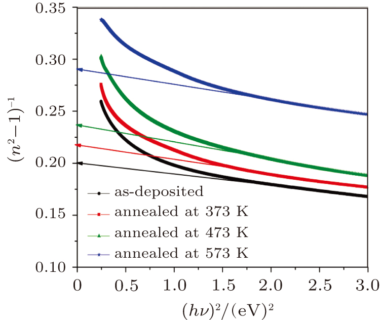
The oscillator parameters such as the dispersion energy (Ed) and the single oscillator energy (Eo) can be determined from the relation between (n2 − 1)−1 and ()2 as displayed in Fig. 11 for the as-deposited and thermally annealed CdS/ZnO thin films. In addition, the infinite frequency dielectric constant, ε, can be estimated. The single oscillator parameters are displayed in Table 2.

Fig. 11. Plots of (n2 − 1)−1 versus ()2 for as-deposited and thermally annealed of CdS/ZnO thin films.

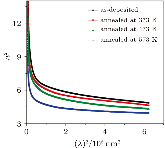
Also, at the low optical frequencies, the relationship between squared refractive index (n2) and squared wavelength (λ2) is given by the following equation[47]

where εL is the lattice dielectric constant, e is the electronic charge, εo is the permittivity of free space, c is the velocity of light, and N/m* is the ratio of free carrier concentration to the effective mass of charge carrier. As shown in Fig. 12, at longer wavelengths the dependence of squared refractive index (n2) on squared wavelength (λ2) for each of the as-deposited and thermally annealed CdS/ZnO thin films is linear. The lattice dielectric constant (εL) is calculated by extrapolating this linear part to zero wavelength and the ratio of free carrier concentration to the effective mass of charge carrier (N/m*) is calculated from the slope of this linear part. These parameters are displayed in Table 2.

Fig. 12. Plots of n2 versus λ2 for as-deposited and thermally annealed of CdS/ZnO thin films.

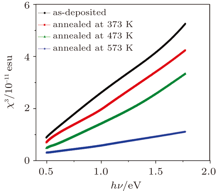
In a system showing a negligible absorption, the third-order nonlinear susceptibility for the as-deposited and thermally annealed CdS/ZnO thin films can be calculated from the following relation[4851]

where A ≈ 10−10 esu is a constant.[4851] The plots of χ(3) versus for the as-deposited and thermally annealed CdS/ZnO thin films are displayed in Fig. 13.

Fig. 13. Spectral behaviors of third-order nonlinear susceptibility, χ(3) for as-deposited and thermally annealed of CdS/ZnO thin films.

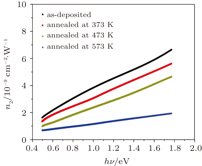
Furthermore, the nonlinear refractive index (n2) can be determined from the relation[51]

The plots of n2 versus for the as-deposited and thermally annealed CdS/ZnO thin films are displayed in Fig. 14. Figures 13 and 14 show that the spectral behaviors of the third-order nonlinear susceptibility and nonlinear refractive index are slightly weakened by annealing up to 573 K. The spectral thermal behavior of χ(3) and n2 follow the same trend as the real part of the refractive index.

Fig. 14. Spectral behaviors of nonlinear refractive index n2 for as-deposited and thermally annealed of CdS/ZnO thin films.

From the above experimental results, it may be concluded that the influences of the annealing temperature on the microstructural (FTIR, XRD, and FESEM), optical and photoluminescence properties of binary nanocomposite materials (CdS/ZnO) thin films can be attributed to physical rather than chemical changes, for this can be explained on the basis of the difference in chemical bonding structure after annealing and the reaction between the atoms of both cadmium and zinc metal. Thus, the nature of chemical bonding among certain constituent atoms should play a significant role in the onset of non-metallic physical properties of quasicrystals bearing transition-metal elements. On the other hand, the self-similar symmetry of the underlying structure gives rise to the presence of an extended chemical bonding network due to a hierarchical nesting of clusters. Also, the dislocation density and the compressive stress induced in the as-deposited CdS/ZnO thin films decrease with annealing temperature increasing.

4. Conclusions

The influences of annealing temperature on the morphological, structural, and optical characteristics of RF sputtered CdS/ZnO thin films are analyzed. The FTIR spectra are verified by the existence of the band centered at 485 cm−1 assigned to Zn–O zinc oxide bond, two bands at 960 cm−1 and 775 cm−1 assigned to the stretching frequency of Cd–S bond and the band at 1150 cm−1 assigned to the S–O stretching vibration of the CdS–ZnO thin films. The XRD analyses of the as-deposited and thermally annealed CdS/ZnO thin films reveal that the films are all amorphous in nature. The FESEM images reveal that the thin films possess uniform distribution of identical nanoparticles in the range of (120 ± 9) nm. Photoluminescence emission spectra of CdS/ZnO thin films show overall decrease in their peak intensities after annealing. The emission peaks can be attributed to the intrinsic defects such as sulfur vacancies, surface states, and oxygen vacancies. The optical band gaps of CdS/ZnO thin films all show a distinct blue shift with temperature increasing up to 473 K, which can be related to the band bending effect. The slight red shift in the band gap at 573 K can be attributed to the band gap narrowing effect through many-body effects. The microstructural and optical properties of the as-deposited and thermally annealed CdS/ZnO thin films are studied to identify and verify the characteristics of CdS/ZnO thin films for optoelectronic applications. Additionally, the estimated third-order nonlinear susceptibility and nonlinear refractive index are observed to be reduced as the annealing temperature increases.

Reference
[1] Rajput J K Purohit L P 2016 Nanosci. Technol. 3 1
[2] Nwanya A C Deshmukh P R Osujib R U Maazad M Lokhande C D Ezema F I 2015 Sens. Actuat. B: Chem. 206 671
[3] McCool N S Swierk J R Nemes C T Schmuttenmaer C A Mallouk T E 2016 J. Phys. Chem. Lett. 7 2930
[4] Kuang W J Li Q Sun Y Chen J Tolner H 2016 Mater. Lett. 178 27
[5] Wang L Wei H Fan Y Liu X Zhan J 2009 Nanoscale Res. Lett. 4 558
[6] Sikarwar S Yadav B C Singh S Dzhardimalieva G I Pomogailo S I Golubeva N D Pomogailo A D 2016 Sensor Actuat. B: Chem. 232 283
[7] Xiong W 2016 Superlattice Microstruc. 98 158
[8] Vishwakarma A K Yadava L 2018 Vacuum 155 214
[9] Fang F Zhao D X Li B H Zhang Z Z Zhang J Y Shen D Z 2008 Appl. Phys. Lett. 93 233115
[10] Vasa P Taneja P Ayyub P Singh B P Banerjee R 2002 J. Phys.: Condens. Matter 14 281
[11] Wang X Liu G Lu G Q Cheng H M 2010 Int. J. Hydrogen Energy 35 8199
[12] Sharma M Jeevanandam P 2012 Mater. Res. Bull. 47 1755
[13] Kozhevnikova N S Gyrdasova O I Vorokh A S Baklanova I V 2014 Nanosyst. Phys. Chem. Math. 5 579
[14] Velanganni S Pravinraj S Immanuel P Thiruneelakandan R 2018 Physica B 534 56
[15] Meng X Q Zhao D X Zhang J Y Shen D Z Lu Y M Fan X W Wang X H 2007 Mater. Lett. 61 3535
[16] Rajeshwar K de Tacconi N R 2001 Chem. Mater. 139 2765
[17] Alivisatos A P 1996 Science 271 933
[18] Anderson M A Gorer S Penner R M 1997 J. Phys. Chem. B 101 5895
[19] Caruso F 2001 Adv. Mater. 13 11
[20] Thambidurai M Muthukumarasamy N Arul N S Agilan S Balasundaraprabhu R 2011 J. Nanopart. Res. 13 3267
[21] Yang X Yang Q Hu Z Guo S Li Y Sun J Xu N Wu J 2015 Sol. Energy Mater. Sol. Cells 137 169
[22] Nayak J Sahu S N Kasuya J Nozaki S 2008 Appl. Surf. Sci. 254 7215
[23] Gao T Li Q Wang T 2005 Chem. Mater. 17 887
[24] Du N Zhang H Chen B Wu J Yang D 2007 Nanotechnology 18 115619
[25] Panda S K Chakrabarti S Satpati B Satyam P V Chaudhuri S 2004 J. Phys. D: Appl. Phys. 37 628
[26] Vasa P Singh B P Ayyub P 2005 J. Phys.: Condens. Matter 17 189
[27] Vanalakar S A Mali S S Suryawanshi M P Tarwal N L Jadhav P R Agawane G L Gurav K V Kamble A S Shin S W Moholkar A V Kim J Y Kim J H Patil P S 2014 Opt. Mater. 37 766
[28] Adegoke K A Iqbal M Louis H Bello O S 2019 Mater. Sci. Energy Technol. 2 329
[29] El-Nahass M M 1992 J. Mater. Sci. 27 6597
[30] Di Giulio M Micocci G Rella R Siciliano P Tepore A 1993 Phys. Status Solidi A 136 K101
[31] El-Nahass M M Atta A A Abd El-Raheem M M Hassanien A M 2014 J. Alloys Compd. 585 1
[32] Hassanien A M Atta A A El-Nahass M M Ahmed S I Shaltout A A Al-Baradi A M Alodhayb A Kamal A M 2020 Opt. Quantum Electron. 52 194
[33] Konstantinov I Babeva T Kitova S 1998 Appl. Opt. 37 4260
[34] Hong R Y Li J H Chen L L Liu D Q Li H Z Zheng Y Ding J 2009 Powder Technol. 189 426
[35] Acharya A Mishra R Roy G S 2010 Lat. Am. J. Phys. Educ. 4 603
[36] Zandi S Kameli P Salamati H Ahmadvand H Hakimi M 2011 Physica B 406 3215
[37] Rawal S K Chawla A K Jayaganthan R Chandra R 2014 Mater. Sci. Eng. B 181 16
[38] Dimova-Malinovska D Nichev H Angelov O 2008 Phys. Stat. Sol. (c) 5 3353
[39] Astinchapa B Laelabadic K G 2019 J. Phys. Chem. Solids 129 217
[40] Beena D Lethy K Vinodkumar R Pillai V M Ganesan V Phase D Sudheer S 2009 Appl. Surf. Sci. 255 8334
[41] Goswami S Sharma A K 2019 Appl. Surf. Sci. 495 143609
[42] Feneberg M Nixdorf J Lidig C Goldhahn R Galazka Z Bierwagen O Speck J S 2016 Phys. Rev. B 93 45203
[43] Ayyub P Vasa P Taneja P Banerjee R Singh B P 2005 J. Appl. Phys. 97 104310
[44] Vanalakar S A Mali S S Suryawanshi M P et al. 2014 Opt. Mater. 37 766
[45] Wemple S H DiDomenico M 1971 Phys. Rev. B 3 1338
[46] Wemple S H 1973 Phys. Rev. B 7 3767
[47] Palik D E 1985 Handbook of Optical Constants of Solids Academic Press 265
[48] Miller R C 1964 Appl. Phys. Lett. 5 17
[49] Wang C C 1970 Phys. Rev. B 2 2045
[50] Tichý L Tichá H Nagels P Callaerts R Mertens R Vlček M 1999 Mater. Lett. 39 122
[51] del Coso R Solis J 2004 J. Opt. Soc. Am. B 21 640