† Corresponding author. E-mail:
Project supported by the Natural Science Foundation of Zhejiang Province, China (Grant No. LY17F010022) and the National Natural Science Foundation of China (Grant No. 61372156).
Dark count is one of the inherent noise types in single-photon diodes, which may restrict the performances of detectors based on these diodes. To formulate better designs for peripheral circuits of such diodes, an accurate statistical behavioral model of dark current must be established. Research has shown that there are four main mechanisms that contribute to the dark count in single-photon avalanche diodes. However, in the existing dark count models only three models have been considered, thus leading to inaccuracies in these models. To resolve these shortcomings, the dark current caused by carrier diffusion in the neutral region is deduced by multiplying the carrier detection probability with the carrier particle current at the boundary of the depletion layer. Thus, a comprehensive dark current model is constructed by adding the dark current caused by carrier diffusion to the dark current caused by the other three mechanisms. To the best of our knowledge, this is the first dark count simulation model into which incorporated simultaneously are the thermal generation, trap-assisted tunneling, band-to-band tunneling mechanisms, and carrier diffusion in neutral regions to evaluate dark count behavior. The comparison between the measured data and the simulation results from the models shows that the proposed model is more accurate than other existing models, and the maximum of accuracy increases up to 31.48% when excess bias voltage equals 3.5 V and temperature is 50 °C.
With the development of the complementary metal–oxide–semiconductor (CMOS) technology,[1,2] single-photon avalanche diode (SPAD) detectors based on this technology have been favored by researchers and have been applied to many fields, including laser ranging,[3] fluorescence lifetime imaging,[4] two-dimensional scanning imaging,[5] and other such applications because of their increased sensitivity, high gain coefficients, and increased response speeds.
However, CMOS technology gives rise to the generation of the dark count that constitutes the inherent noise in SPADs. Accordingly, this noise may cause photon counting errors and can considerably restrict the performances of SPAD detectors. To design the peripheral circuits of SPADs and ensure normal SPAD operations, a precise behavioral model for simulating the statistical characteristics of the dark count must be established. However, the early models described only the current–voltage (I–V) characteristics and ignored the statistical behavior of the dark count in SPADs.[6,7] Subsequently, other reports[8,9] proposed a behavioral model to predict the dark count. However, this simulation model considers only the thermal dependence of the dark count and ignores the electric-field-dependent tunneling effects. The effect of band-to-band tunneling (BTBT) on the dark count was also considered for the first time in Ref.[10], but the trap-assisted tunneling (TAT) mechanism was ignored. Recently, a comprehensive and accurate dark count model was proposed.[11,12] However, studies have shown that carrier diffusion in the neutral region can also cause the dark count[13,14] that has been ignored in the aforementioned dark count models.
In the present study, the dark current caused by carrier diffusion in the neutral region is deduced by multiplying the carrier detection probability with the carrier particle current from three neutral regions at the boundary of the depletion layer. Therefore, based on previous dark count modeling studies in Refs. [11,12], a more accurate theoretical and statistical model is deduced that simultaneously considers the effects of thermal generation, carrier diffusion, and TAT and BTBT mechanisms for the first time. Furthermore, unlike the existing statistical models of dark current, which consider the avalanche triggering probability and electric field strength as constants under the same excess bias voltage that is denoted as Vex in this paper, the parameters of the proposed theoretical dark count model are varied with depth, obtained by extracting the model parameters of the SPAD device as a function of depth of the depletion region under the same excess bias voltage, thereby improving the accuracy of the proposed dark count model. Finally, the developed theoretical model for the dark counts was implemented with Verilog-A (a hardware description language) to formulate a statistical behavioral model.
The rest of this paper is organized as follows. In Section
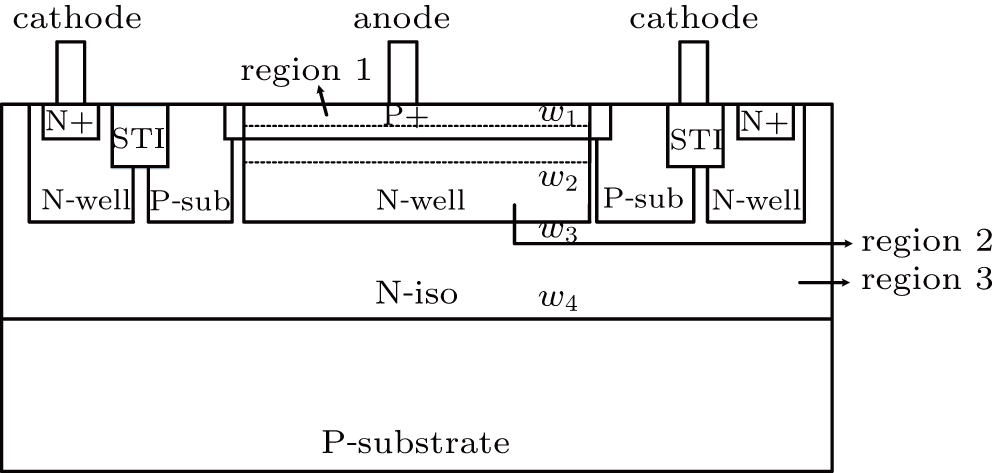
The device model used in this study is based on a standard CMOS process in an effort to form an SPAD with a virtual guard-ring structure, as shown in Fig.
Dark counts are generally caused by device defects[14] and effectively correspond to the inherent noise in CMOS technology. In the absence of light, the dark carriers caused by the noise itself will produce the same avalanche as the photon-generated carrier and result in photon counting deviations. The dark counts are usually expressed as the dark count rate (DCR), i.e., the number of dark count occurrences per second (Hz). Studies have shown that dark count generation is mainly affected by four factors: Shockley–Read–Hall (SRH) thermal generation, TAT, BTBT,[8–12] and carrier diffusion.[13,14] The contributions from each of these four generating mechanisms are described in the following subsections.
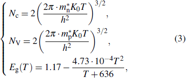
In general, the SRH theory is used to determine the rate of thermally generated carriers. In the depletion region, the density of electrons and holes are both much lower than the intrinsic carrier concentration. So the rate of carrier generation due to thermal generation can be expressed as[10]




The rate of carrier generation caused by TAT can be calculated by the field-effect-enhanced SRH model based on the following formula:[11]

The rate of carrier generation due to BTBT can be given by the Hurkx model according to the following formula:[16]

The overall rate of carrier generation in the depletion region can be expressed as


The minority carriers in the neutral regions will diffuse to the edge of the depletion region, which can additionally cause the dark counts. We define the undepleted P+ layer as region 1, the undepleted N-well layer as region 2, and the N-iso layer as region 3. Based on the carrier diffusion theory discussed in Ref. [19], we conduct the deduction in the following.
The dark count caused by electron diffusion in region 1 is equal to the electron detection probability multiplied by Collectione that is the electron particle current at the boundary of the depletion layer, and expressed by

Similarly, the dark counts in regions 2 and 3 are equal to the hole detection probability multiplied by Collectionh that is the hole particle current at the boundary of the depletion layer, i.e.,


The diffusion length in Eqs. (

In summary, the dark count caused by carrier diffusion in the neutral region is the sum of the dark count caused by carrier diffusion in region 1, in region 2, and in region 3 and can be expressed by

According to the above discussion, we can formulate the proposed model of dark counts as

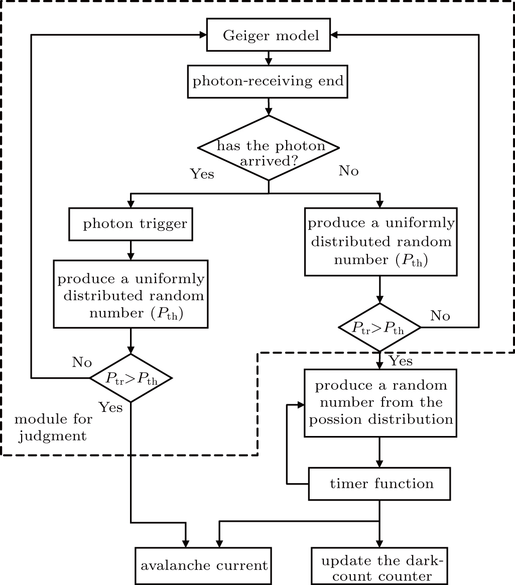
After successfully constructing the theoretical and statistical models of the dark counts, the behavioral model based on Verilog-A is built to describe the behavioral character of the dark counts in SPAD. This model includes five modules as shown in Fig.
The judging module evaluates whether or not a dark count occurs. In the random number module the Poisson distribution is used to produce a random number. The timer function calls the random number to mark the moment at which a dark count occurs. The equivalent circuit model of SPAD generates a large current caused by the dark counts. The dark count counter module counts the number of dark counts. The logical relationships among the modules are schematically shown in Fig.
When the SPAD detector works in the Geiger mode, the judgment module detects the voltage of the photon-receiving end to judge whether or not the photon has arrived. If the photon has arrived, the voltage of the photon-receiving end is high, and if not, the voltage of the photon-receiving end is low. No matter whether the photon has arrived, the judgment module generates a random number to simulate the actual probability of occurrence, which follows a uniform distribution[10] expressed as Pth, and the function $redis_uniform() in Verilog-A is used to generate these random numbers. The probability of triggering a carrier avalanche Ptr is then calculated from Eq. (

In most of the existing statistical dark count models, the avalanche triggering probability (including the hole triggering and electron triggering probabilities) and the electric field strength are obtained from empirical formula and are both considered to be constant for the same excess bias voltage. However, the changes of the corresponding parameter values at different depths of the depletion region under the same excess bias voltage are ignored.[8–10] In the present study, the Silvaco technology computer-aided design (TCAD) tool is used to simulate the SPAD device model to accurately extract the avalanche triggering probabilities and electric field strengths at different depths in the depletion region. Accordingly, using MATLAB tools, these extracted values are fitted with respect to the depletion depth. The obtained fitting functions are incorporated into Eqs. (
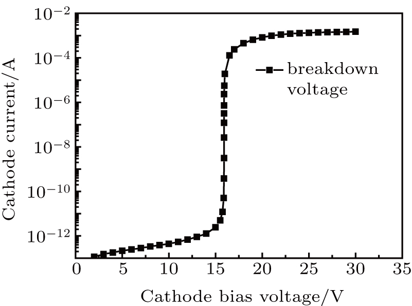
To ensure that the simulation results are as close as possible to the results obtained from the actual device reported in Ref.[15] and to extract more accurate physical parameters, the breakdown voltage is calibrated based on parameter adjustments for the SPAD device. These parameters are listed in Table
| Table 1. Key parameters of Verilog-A model of SPAD. . |
The distributions of the hole and electron triggering probability and the distribution of the electric field strength as a function of depth at different excess bias voltages are shown in Fig.
 | Fig. 5. Extracted (a) hole trigger probability, (b) electron trigger probability, and (c) electric field strength at different depths. |
Figures
The proposed dark count statistical model is implemented by using the behavioral hardware description language of Verilog-A according to the flowchart in Fig.
Table
| Table 2. Simulated DCR as a function of excess bias voltage at 26.7 °C. . |
Table
| Table 3. Simulation of DCR as a function of temperature at Vex = 3.5 V. . |
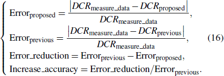
Two indices are calculated to evaluate the proposed dark current model, where the variable Errorproposed represents the error of the proposed model relative to the measured data. The variable Errorprevious indicates the error of the existing model in Refs. [11,12] relative to the measured data. The variable Errorreduction is the decrement in the error in the existing model relative to that of the model proposed in Refs. [11,12], and the parameter Increased_accuracy is the increment in the accuracy of the proposed model relative to that of the existing model.
Tables
In this study, a statistical model for the dark current is proposed to simulate the behavior of the dark current more accurately than the existing models. The proposed model is primarily based on this existing theoretical model but also reflects the effect of carrier diffusion. The developed statistical model of the dark current is implemented with Verilog-A. Correspondingly, the Cadence Spectre simulations that invoked this behavioral model confirm the validity of the proposed model. This is the first time that the effect of carrier diffusion on dark counts has been considered, where the important parameters in the proposed model are varied with the depth of the depletion region of SPAD device. The simulation results show that the DCRs from proposed method are closer to the measured data than those from the existing models. Effectively, the relative error is 2.39% lower than those from the existing models, and its accuracy is 31.48% higher than the existing models, when excess bias voltage equals 3.5 V and temperature is 50 °C. The proposed dark current model can offer a beneficial reference for accurately simulating the physical characteristics of SPADs and in turn, for designing the peripheral circuit for SPADs.
| [1] | |
| [2] | |
| [3] | |
| [4] | |
| [5] | |
| [6] | |
| [7] | |
| [8] | |
| [9] | |
| [10] | |
| [11] | |
| [12] | |
| [13] | |
| [14] | |
| [15] | |
| [16] | |
| [17] | |
| [18] | |
| [19] |


