Effect of initial crystallization temperature and surface diffusion on formation of GaAs multiple concentric nanoring structures by droplet epitaxy
Wang Yi1, 2, Guo Xiang1, 2, 3, Wei Jiemin2, Yang Chen1, 3, 4, Luo Zijiang1, 4, Wang Jihong1, Ding Zhao1, 2, 3, †
College of Big Data and Information Engineering, Guizhou University, Guiyang 550025, China
Power Semiconductor Device Reliability Research Center of the Ministry of Education, Guizhou University, Guiyang 550025, China
Key Laboratory of Micro-Nano-Electronics of Guizhou Province, Guiyang 550025, China
School of Information, Guizhou University of Finance and Economics, Guiyang 550025, China


† Corresponding author. E-mail: zding@gzu.edu.cn

Project supported by the National Natural Science Foundation of China (Grant Nos. 61564002 and 11664005), the Science and Technology Foundation of Guizhou Province, China (Grant No. QKH-[2017]1055), and Guizhou University Talent Foundation (Grant No. GDJHZ-[2015]23).

Abstract

GaAs multiple concentric nano-ring structures (CNRs) are prepared with multistep crystallization procedures by droplets epitaxy on GaAs (001) to explore the influence of different initial crystallization temperatures on CNRs morphology. Atomic force microscope (AFM) images show that GaAs nanostructures are more likely to form elliptical rings due to diffusion anisotropy. Meanwhile, with the increase of initial crystallization temperature, the inner ring height and density of CNRs are increased, and outer rings are harder to form. In addition, the mechanism of formation of CNRs is discussed by classical nucleation theory and diffusion theory. The method can be used to calculate the diffusion activation energy of gallium atoms (0.7±0.1 eV) on the GaAs (001) surface conveniently.

1. Introduction

In nearly a decade, numerous efforts have been devoted to low-dimensional semiconductor nanostructures due to the growing interest in both unique physical properties and their potential application in nanodevices.[13] Concentric quantum ring nanostructures make it possible to explore magneto–optical excitation based on Rashba spin–orbit interaction. Concentric quantum ring has a unique dispersion of magnetic field energy level. The energy dispersion of excitons with different radii of ring is different because the total angular momentum of the ground state changes from zero to non-zero by increasing the magnetic field, unlike quantum dots.[4,5] Concentric quantum rings offer the control of effective coupling of direct–indirect excitons, it could pave the way to multiple level states devices with switchable interaction in the research of semiconductor-based quantum computational devices.[6] More and more researchers are attracted to determine the geometry of concentric quantum rings carefully.

To date, many theoretical contributions have been made on the formation of nanostructures, such as nano holes, quantum dot rings, concentric quantum rings, and quantum dots that formed from gallium droplets on GaAs (001).[7] Spirina studied the process of metal droplet formation and motion under the Langmuir evaporation conditions through Monte Carlo simulation.[8] Barseghyan investigated the Josephson effect in quantum structures by performing the numerical renormalization group calculations.[9] However, only a few experimental results on the GaAs concentric quantum rings (CNRs) by droplet epitaxy (DE) are reported, the details of the processes controlling the shapes and sizes of nanostructure have not been systematically investigated yet.[10,11] There still has not been well understood on the influences of crystallization temperature and time on the formation of GaAs CNRs.

In this paper, GaAs multiple concentric nano-ring structures (CNRs) are prepared by multistep crystallization procedures by droplets epitaxy to research the influence of different initial crystallization temperatures on CNRs morphology. The theoretical physical model and experimental results are combined to explore the formation mechanism of CNRs. In addition, the method gives a convenient way to calculate the diffusion activation energy of gallium atoms on the GaAs (001) surface.

2. Samples and experimental

The experiments were carried out in a molecular beam epitaxy (MBE) system (Omicron) under ultra-high vacuum (UHV) (4 × 10⁻⁹–8 × 10⁻⁹ Torr (1 Torr = 1.33322×10² Pa) throughout). The substrates used in experiments were ‘epi-ready’ n-type (Si doped 10−18 cm−3) GaAs (001) wafer. After the oxide desorption at 580 °C, A 1000-nm thick GaAs buffer layer was first grown at a growth rate of 0.3 monolayer (ML)/s and substrate temperature of 560 °C. The GaAs layer was annealed without changing substrate temperature for 40 min to prepare the atomically smooth surface under 9-μTorr As4 beam equivalent pressure (BEP).

To research the formation mechanisms and diffusion anisotropy of multiple structures of GaAs CNRs, the substrate temperature was then decreased to 350 °C and the arsenic valve closed. Subsequently, we performed a sequential four-steps procedure.

Step 1 An equivalent amount of 15 MLs of gallium at 350 °C in absence of arsenic pressure.

Step 2 An arsenic flux supply of 5.6 μTorr at different initial crystallization temperatures (240 °C; 250 °C; 260 °C; 270 °C) for 10 s, after that, the arsenic valve closed.

Step 3 Increase the crystallization temperature to 270 °C and an arsenic flux is supplied with the same intensity as in Step 2 for 10 s.

Step 4 The arsenic flux without changing is supplied for 20 min at 290 °C to ensure the complete crystallization of the deposited gallium atoms.

The reflection high-energy electron diffraction (RHEED) pattern changes during the every growth experiment, as described in Ref. [12], allowing us to assess the structural evolution of CNRs which happened during the growth. After the above procedure, the morphology of samples was obtained by atomic force microscope (AFM) at room temperature.

3. Results and discussion
3.1. Effect of initial crystallization temperature on formation of GaAs CNRs

Under the arsenic flux, CNRs evolve starting from gallium droplets to concentric quantum rings at different initial crystallization temperatures according to experimental arrangement in Step 2 (240 °C; 250 °C; 260 °C; 270 °C). The AFM images of CNRs obtained from the deposited droplets after crystallization at different temperature are shown in Figs. 1(a)1(c), respectively. Through the four-step experiment, the atoms inside gallium droplets diffuse outward, crystallize into rings with arsenic atoms and formed a three-layer concentric ring nanostructure (T-CNRs). The density of GaAs nano-rings increases from 4.3 × 108 cm−2 to 7 × 108 cm−2 with the increase of the initial crystallization temperatures in Step 2. We speculate this change is due to different nucleation processes. In our experiment, the initial nucleation of gallium droplet was kept at the same temperature (350 °C), but the droplets were split when the sequential crystallization temperatures change in Step 2. The higher the temperature for sequential crystallization, the more favorable it will be for the droplets to split and re-nucleate, and it may lead to an increase in the CNRs density, as shown in Figs. 1(a)1(c).
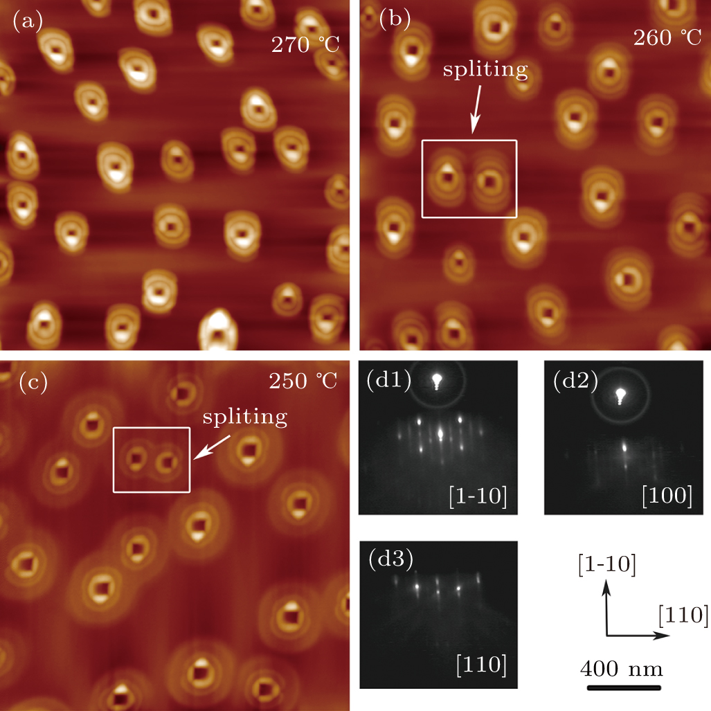
Fig. 1. AFM images (a)–(c) and RHEED patterns (d1)–(d3) of the samples with different initial crystallization temperatures at Step 2 (270 °C; 260 °C; 250 °C) respectively.

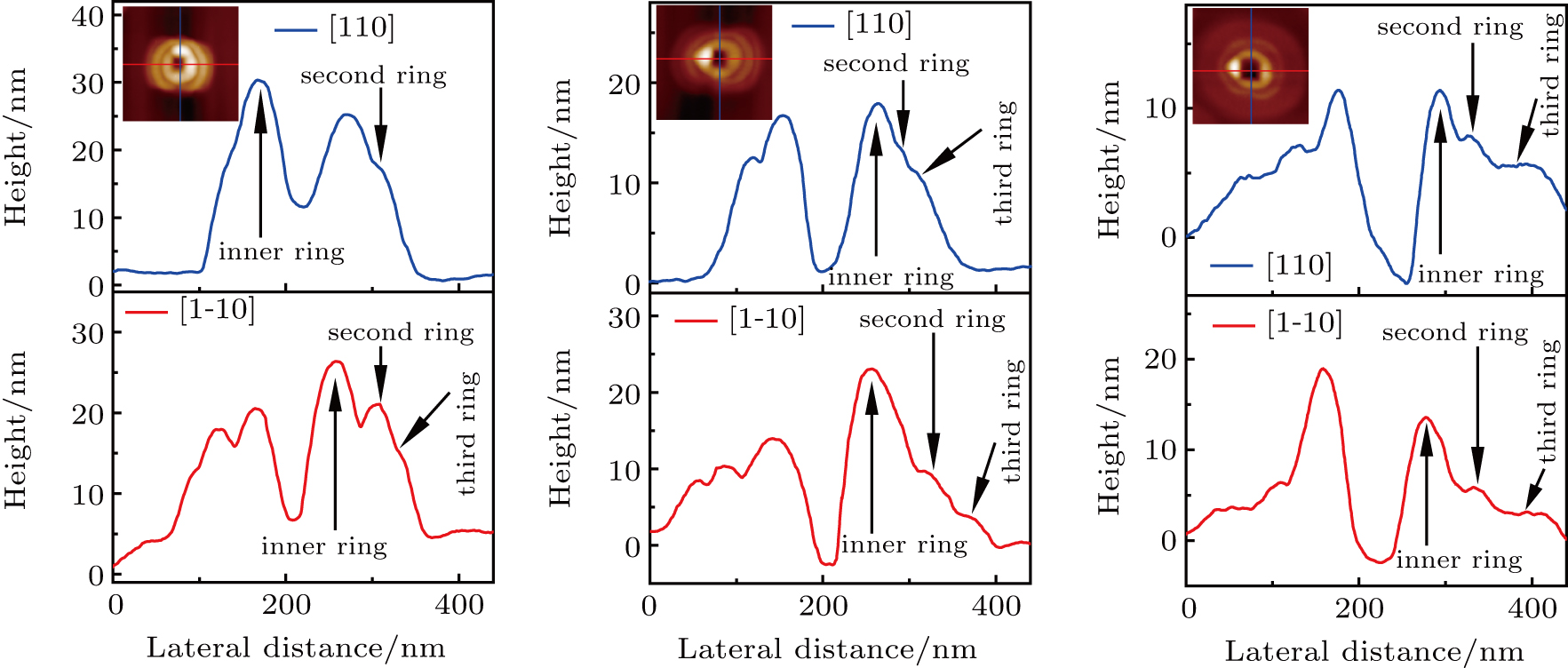
The RHEED patterns (in panels (d1)–(d3)) show that there is still weak reconstruction on the substrate surface after the crystallization, which indicates that gallium atoms diffused outward and crystalized with arsenic flux in layer by layer growth mode to form rings that kept the reconstruction of substrate.[13] In order to obtain quantitative morphology change information in our experiments, each GaAs CNRs was selected from Figs. 1(a)1(c) to measure the average height and radius of each layer ring, the AFM profile line analysis of each nanostructures along the [110] direction (blue line) and the [1-10] (red line) is performed in Figs. 2(a)2(c). Comparing the profile line measurement results, a good rotational symmetry of GaAs triple CNRs (T-CNRs) is observed at 250 °C with the inner, second, and third rings with average heights of about 15 nm, 12 nm, and 7 nm respectively, and with average diameters about 76 nm for the inner rings, 119 nm for second rings, and 184 nm for the third rings. Meanwhile, the higher initial crystallization temperature causes the atoms in the droplets to form a higher inner ring, which causes the atoms to diffuse outward across the inner ring, overcoming a larger potential barrier. It makes the structure of the second ring less obvious, especially in the [110] direction (this is caused by the anisotropy of surface diffusion of gallium atoms).

Fig. 2. Upper panel: AFM profiles along the [110] direction (insets show 450 nm × 450 nm AFM images of the fabricated nanostructures for samples in Figs. 1(a)1(c). Lower panel: AFM profiles along the [1-10] direction.

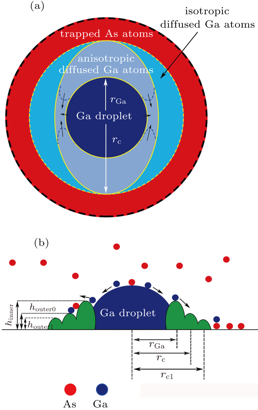
Taking into account the AFM images of samples, we propose a formation mechanism of CNRs based on the arsenic atoms adsorption and diffusion anisotropy of gallium atoms. Figure 3 schematically illustrates diffusion of gallium atoms and trapped arsenic atoms. According to the formation mechanism of CNRs, we can divided the surface into three regions, the first is the region of gallium droplets, the second is the anisotropic diffusion (or isotropic diffusion) region of gallium atoms, and the last is trapped region of arsenic atoms as shown in Fig. 3(a). The gallium atoms at boundary of droplet are crystallized by the arsenic atoms deposited on droplet surface. Also, the diffused gallium atoms can crystallized with the trapped arsenic atoms at the periphery region of gallium atoms. However, because of the short crystallization time and the increasing substrate temperature during each crystallization process, some of the free gallium atoms not trapped by the arsenic atom diffuse outward and cross the boundary to form the second or third ring on the outer side. Due to the anisotropy of surface diffusion, gallium atoms are more likely to diffuse into a ring in the direction of [1-10], thus forming an oval outer ring.[14] The higher the temperature is, the more obvious the anisotropy is (see the insets in Figs. 2(a)2(c)). To explain the differences in structure formation, we can define some parameter in the crystallization with different growth regimes, such as the third ring radii (rc1); the second ring radii (rc); inner ring radii (rGa); height of the inner ring (hinner); height of the second ring (houter0); height of the third ring (houter1), as shown in Fig. 3(b).

Fig. 3. (a) Schematic drawing of diffusion of gallium atoms and trapped arsenic atoms. (b) Schematic drawing of the formation process of CNRs. Definition of the third ring radii (rc1); the second ring uadius (rc); the inner ring radius (rGa); height of the inner ring (hinner); height of the second ring (houter0); height of the third ring (houter1).

According to nucleation theory by Venables,[1416] the equations for cluster density (nx) are of the form

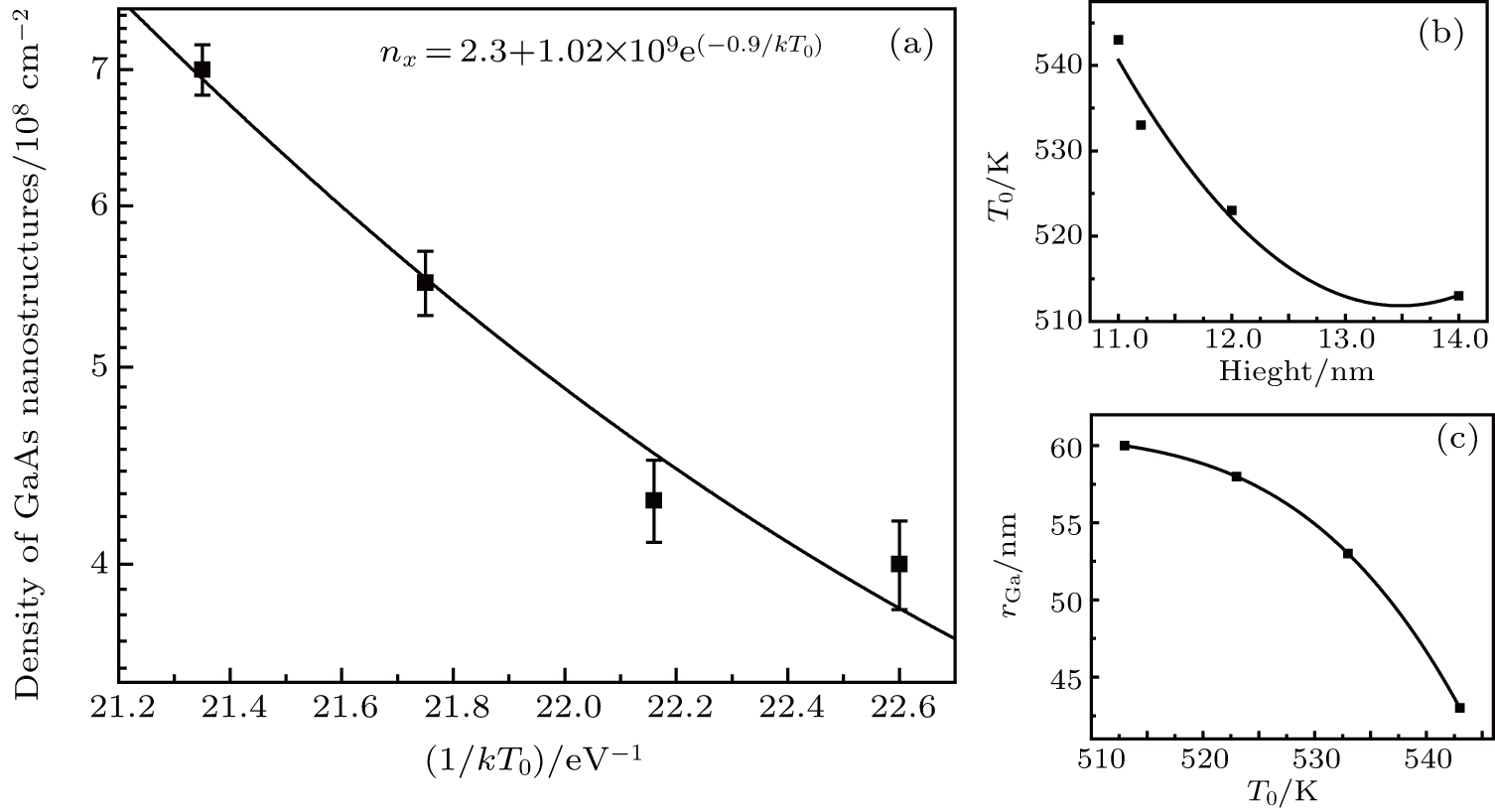
where R is the deposition rate of gallium, v is an atomic vibration frequency, p are tabulated in Refs. [15] and [16] elsewhere for two-dimensional (2D) and three-dimensional (3D) clusters in various condensation regimes,[15,16] k is the Boltzmann constant; ΔE is the total energy required for nucleation of CNRs which is closely related to adsorption (Ea), diffusion (Ed) and activation (EGa) energies in Eq. (2). T is the crystallization temperature. The droplet density statistics are carried out based on the experimental results, and the statistical values, as shown in Fig. 4(a), are fitted according to Eq. (1). From the fitting curve, the value of ΔE can be calculated to be −0.91 eV.

Fig. 4. (a) Density of GaAs CNRs plotted as a function of initial crystallization temperature (T0). The line represents exponential fit to the data on Eq. (1); (b) hinner versus initial crystallization temperature; (c) rGa versus initial crystallization temperature.

In addition, we measured the average height and radius of the inner ring, statistically averaged the measured results and plotted them, as shown in Figs. 4(b)4(c). It is found that with the increase of temperature, the inner ring radius decreases while the height increases, It is not hard to see that the higher the initial crystallization temperature is, the easier it is for the large droplets to split, and more atoms in the droplets are activated to form an inner ring, so that the higher the height of the ring, the smaller the radius of the ring. This is consistent with the change trend of structure density and confirms the theory we put forward earlier in Fig. 3.[17]

3.2. Thermodynamics of surface diffusion during GaAs nano-rings formation

According to Fick law and the growth model of CNRs,[18] we can retrieve the size of diffusion of gallium atoms as follows:

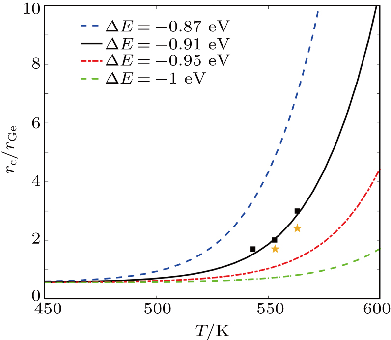
where w(x) represents the Lambert W function which is also called the omega function and is the inverse function of f(W) = WeW. Because w(x) is a monotonically increasing function. D0 is the prefactor, v0 and v1 are the thermal vibration frequencies for the upward direction and lateral direction, α0 is the space between surface sites, C0 refers to the concentration of Ga atoms on the droplet boundary, h0 is the thickness of the monolayer. The value of rc determines the second boundary of final GaAs CNRs, and the size of gallium droplet determines the inner ring of GaAs CNRs. Thus, the height of concentric rings of GaAs CNRs can be controlled through regulating crystallization temperature and the intensity of arsenic flux (P). The rc/rGa in [1-10] direction (black square dots) and [110] direction (orange pentagram dots) of Figs. 2(a)2(c) are substituted into Eq. (3), respectively, and the temperature versus rc/rGa relationship is drawn and fitted by exponential function (see Fig. 5). The value of ΔE can be retrieved to be −0.91 eV in [1-10] direction and −0.92 eV in [110] direction in our experiment. This is close to the results in Ref. [18] and supported by the value of ΔE fitted by Eq. (1). The gap in the activation energy of diffusion in different crystal directions obviously leads to a decrease in the ability of atoms to diffuse along [110] directions. This also affects the shape of the ring and the outer ring. Meanwhile, as can be seen from Fig. 5, the value of ΔE influences the change of rc/rGa. With ΔE decreases, the droplet becomes more stable, gallium atoms in the droplet need more energy to diffuse out of the boundary. So, it becomes more and more difficult for the droplets to diffuse to form an outer ring.

Fig. 5. The rc/rGa versus crystallization temperature with various ΔE (−0.87 eV; −0.91 eV; −0.95 eV; −1 eV) by Eq. (3).

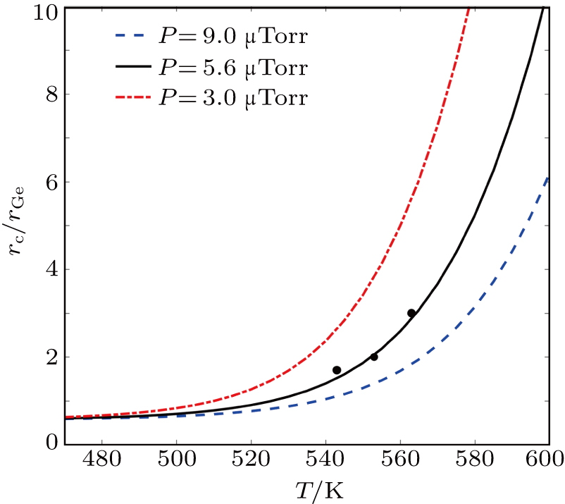
For this model, we can further discuss the effect of arsenic pressure on outer ring formation. With arsenic pressure as a parameter (ΔE is −0.91 eV), the fitting of the Eq. (3) was carried out and the results were shown in Fig. 6. The results show that as the arsenic pressure increases, the growth of rc/rGa slows down significantly. This is because the increase of arsenic atoms will hinder the outward diffusion of gallium atoms and makes the formation of the outer ring more difficult. Therefore, low arsenic pressure and appropriate temperature is conducive to the formation of the outer ring.

Fig. 6. rc/rGa versus crystallization temperature with various arsenic pressures (9 μTorr; 5.6 μTorr; 3 μTorr) by Eq. (3).

To confirm the formation mechanism of GaAs CNRs and to generalize the growth model, we extended one more crystallization step performed at different crystallization temperatures by the techniques previously described to realize four concentric nanorings (F-CNRs) grown. 15-MLs gallium is deposited at 350 °C and four subsequent crystallization processes were performed at 240 °C, 270 °C, and 280 °C for 10 s respectively and at 290 °C for 20 min to ensure full crystallization of the F-CNRs. The AFM images and line profile, showing the good rotational symmetry F-CNRs, are observed in Figs. 7(a)7(b). The realization of F-CNRs shows the success of the formation mechanism that we proposed in GaAs CNRs clearly. A regular behavior was observed in the dependence of each ring radius on crystallization temperature in Fig. 7(b). It offers a possibility to finely tune the radius and height of each ring in CNRs by a suitable choice of the each crystallization temperature, as a growth parameter for CNRs.

Fig. 7. (a) AFM image of as-grown sample with four-CNR; (b) half AFM profiles along the [110] direction; (c) hinner/houter(n) versus crystallization temperature.

We can extend the formula for the relation between the height of the reference outer ring and inner ring in Ref. [19] to a more general case.[19] The ratio between the heights of each layer of outer ring (houter(n)) and inner ring (hinner) could be closely proportional to

The crystallization temperature dependence agrees well with the model of GaAs CNRs growth we proposed, where the radius and height of the outer ring are determined by the diffusion limited process from the gallium droplet and inner ring during the crystallization process. The height of rings measured in the experiment is substituted into Eq. (4), and the curve is fitted in Fig. 7(c). The experimental data are in good agreement with the model trends. The value of EdEa can be calculated as −0.21(±0.1) eV.

Table 1.

Comparation of values in scientific literature for EGa.

.

This result can be further substituted into Eq. (2) for EGa, we calculate the value of EGa being 0.7 ± 0.1 eV. In Table 1, the different results are compared for EGa retrieved from various scientific articles.[2023] Our value of EGa agrees well with the result by Deluca.[23] The agreement demonstrates the validity of the diffusivity parameter set obtained in this work. However, the great gap between our result and the published result by Neave might because the RHHED is involving an averaged result over a large area.

It should be pointed out that the previous model by Koshiba did not take into account of the time consumed when the temperature rises or drops in the actual experiment, which may lead to the extension of the diffusion distance, and thus may cause a certain error between the result we solved and the theoretical result of Koshiba. Also, the result of our model is an average that ignores the diffusion anisotropy. As the temperature increases, more obvious anisotropy will lead to more and more errors between the experimental and the theoretical results.

4. Conclusions

In conclusion, the GaAs CNRs were fabricated by droplet epitaxy. We proposed a growth model based on the surface diffusion of gallium atoms at various initial crystallization temperatures and interpreted the growth mechanism on the basis of the morphological evolution of the CNRs and the diffusion of gallium atoms by the model we used. AFM images show that GaAs nanostructures are more likely to form elliptical rings due to diffusion anisotropy. Meanwhile, with the increase of initial crystallization temperature, the inner ring height and density of CNRs increased, and outer rings are harder to form. In addition, the mechanism of the formation of CNRs was discussed by classical nucleation theory and diffusion theory and calculated the diffusion activation energy of gallium atoms (0.7 ± 0.1 eV) on the GaAs (001) surface. The reliable determination of the diffusion activation energy of gallium atoms on GaAs (001) will provide an effective control way to design and fabricated GaAs CNRs.

Reference
[1] Barseghyan M G Manaselyan A K Larozec D Kirakosyan A A 2016 Physica 81 31
[2] Zhao Z Y Min Y Huang Y Y 2019 Physica 114 113589
[3] Li H D Wang Y Liu S H Kang X B Ding J Hao H S 2018 J. Appl. Phys. 124 085103
[4] Zhao X Zheng J Yuan R Y Guo Y 2019 Curr. Appl. Phys. 19 447
[5] Somaschini C Bietti S Koguchi N Sanguinetti S 2009 Nano Lett. 9 3419
[6] Dias da Silva L G G V M Villas-Boas J Ulloa S E 2007 Phys. Rev. 76 155306
[7] Yi G Y Wang X Q Gong W J Wu H N Chen X H 2016 Phys. Lett. 380 1385
[8] Barseghyan M G Kirakosyan A A Laroze D 2017 Opt. Commun. 383 571
[9] Spirina A A Shwartz N L 2019 Mat. Sci. Semicon. Proc. 100 319
[10] Boonpeng P Jevasuwan W Nuntawong N Thainoi S Panyakeow S Ratanathammaphan S 2011 J. Cryst. Growth 323 271
[11] Mano T Kuroda T Sanguinetti S Ochiai T Tateno T Kim J Noda T Kawabe M Sakoda K Kido G Koguchi N 2005 Nano Lett. 5 425
[12] Somaschini C Bietti S Sanguinetti S Koguchi N Fedorov A 2010 Nanotechnology 21 125601
[13] Somaschini C Bietti S Fedorov A Koguchi N Sanguinetti S 2010 Nanoscale Res. Lett. 5 1865
[14] Venables J A Persaud R Metcalfe F L Milne R H Azim M 1994 J. Phys. Chem. Solids 55 955
[15] Venables J A 1987 Phys. Rev. 36 4153
[16] Venables J A Spiller G D T Hanbucken M 1984 Rep. Prog. Phys. 47 399
[17] Li Z H Ding Z Tang J W Wang Y Luo Z J Ma M M Huang Y B Zhang Z D Guo X 2019 Acta Phys. Sin. 68 183601 in Chinese
[18] Li X L 2010 J. Phys. Chem. 114 15343
[19] Li X L 2013 J. Cryst. Growth 377 59
[20] Neave J H Dobson P J Joyce B A Zhang J 1985 Appl. Phys. Lett. 47 100
[21] Koshiba S Nakamura Y Tsuchiya M Noge H Kano H Nagamune Y Noda T Sakaki H 1994 J. Appl. Phys. 76 4138
[22] Labella V P Bullock D W Ding Z Emery C Harter W G Thibado P M 2000 J. Vac. Sci. Technol. 18 1526
[23] Deluca P M Lananda J G C Barnett S A 1999 Appl. Phys. Lett. 74 1719