† Corresponding author. E-mail:
Project supported by the National Natural Science Foundation of China (Grant Nos. 11775191, 61404115, 61434006, and 11475256) and the Promotion Funding for Excellent Young Backbone Teacher of Henan Province, China (Grant No. 2019GGJS017).
An anti-radiation structure of InP-based high electron mobility transistor (HEMT) has been proposed and optimized with double Si-doped planes. The additional Si-doped plane under channel layer has made a huge promotion in channel current, transconductance, current gain cut-off frequency, and maximum oscillation frequency of InP-based HEMTs. Moreover, direct current (DC) and radio frequency (RF) characteristic properties and their reduction rates have been compared in detail between single Si-doped and double Si-doped structures after 75-keV proton irradiation with dose of 5 × 1011 cm−2, 1 × 1012 cm−2, and 5 × 1012 cm−2. DC and RF characteristics for both structures are observed to decrease gradually as irradiation dose rises, which particularly show a drastic drop at dose of 5 × 1012 cm−2. Besides, characteristic degradation degree of the double Si-doped structure is significantly lower than that of the single Si-doped structure, especially at large proton irradiation dose. The enhancement of proton radiation tolerance by the insertion of another Si-doped plane could be accounted for the tremendously increased native carriers, which are bound to weaken substantially the carrier removal effect by irradiation-induced defects.
In nearly several decades, many effective measures have been taken to extend Moore’s law, such as advanced micro/nano-fabrication technologies, novel materials and structures.[1–3] Because of high carrier sheet density, high carrier peak drift velocity, and low-field mobility in InGaAs channel, InAlAs/InGaAs InP-based high electron mobility transistors (HEMTs) have stood out and become competitive alternatives with high frequency, low noise figure, superior gain performance, and so on.[4–6] Furthermore, benefiting from electron beam lithography (EBL) and molecular beam epitaxy (MBE) techniques, the current gain cut-off frequency (fT) and maximum oscillation frequency (fmax) of InP-based HEMTs have been reported to be over than 700 GHz[7] and 1 THz,[8] respectively. Consequently, InP-based HEMTs become as potential candidates for various high speed circuits of transceiver systems in space applications, such as national defense, aerospace, and satellite radar.[9]
In harsh space environment, various high-energy particles and rays will inevitably lead to performance deterioration of devices and even abnormality of electronic systems.[10,11] Especially, proton is one of the main particles in space irradiation environment. Considering mature high technology, low manufacturing cost, and broad usage, researches about proton irradiation effect and hardness techniques are mainly concentrated on Si-based complementary metal–oxide–semiconductor transistor (CMOS) and silicon on insulator (SOI) devices.[12,13] Nevertheless, there are some existing exploratory research on the proton irradiation effects of the various III–V materials devices.[14–17] As a result, the degradation degree of the device characteristics after proton irradiation is directly related to the amount of vacancy defects which are caused by displacement effect, and this damage mechanism has gained wide consensus.[18]
The reliability research of III–V devices about proton irradiation rarely involves anti-radiation device structure and technology techniques. Admittedly, some anti-radiation measures have been proposed yet for III–V devices based on the above proton irradiation damage mechanism and hetero-junction structure, that are the reduction of the body-traps in materials or substitution for current materials with high displacement threshold energy.[19] However, these irradiation hardness techniques will involve enormous constraint from either epitaxy technology or lattice mismatch.
In this paper, InP-based HEMT structure with double Si-doping planes has been put forward and optimized to increase the native carrier concentration and thus improve the proton irradiation tolerance. The DC and RF characteristics of InAlAs/InGaAs InP-based HEMTs with single and double Si-doped plane have been investigated comprehensively by two-dimensional digital simulation. Additionally, their properties of radiation hardness have been studied in detail before and after 75-keV proton irradiation with dose of 5 × 1011 cm−2, 1 × 1012 cm−2, and 5 × 1012 cm−2.
Figure
 | Fig. 1. Schematic cross-section of InP-based HEMTs: (a) single Si-doping plane; (b) double Si-doping plane. |
Reasonable physical models are used to describe the device performances, including hydrodynamic transport model, Shockley–Read–Hall recombination, Auger recombination, radiative recombination, density gradient model, and high field-dependent mobility. And, the hydrodynamic transport model precisely describes many non-equilibrium conditions such as quasi-ballistic transport in thin regions and velocity overshoot effect in depleted regions. Shockley–Read–Hall recombination, Auger recombination, and radiative recombination models are adopted to describe carrier exchange process with the impurity defects in the band-gap. The density gradient model of eQuantumPotential is introduced to depict the quantum effect of 2DEG in InGaAs channel region. The doping and high field-dependent mobility model is used to describe the degradation of electron mobility. Moreover, the irradiation-induced vacancies by displacement effect after proton irradiation are considered self-consistently through solving Poisson and current continuity equations as follows:[22,23]


With the increasing of proton energy, the ultimate stopping position of incident protons in target object will undoubtedly transform from gate metal to hetero-junction layer, and eventually protons will pass through the entire material layers. Consequently, the number of induced defects in hetero-junction region increases firstly and reaches the largest value at about 75 keV.[24] To make a comprehensive impact of proton irradiation on device, the incident proton energy was set as 75 keV with dose of 5 × 1011 cm−2, 1 × 1012 cm−2, and 5 × 1012 cm−2.
The output drain current (IDS) versus drain–source voltage (VDS) characteristics of two structures are assessed before and after 75-keV proton irradiation, as shown in Fig.
 | Fig. 3. Reduction rates of saturation output drain current for devices with single Si-doped plane and double Si-doped plane. |
Figure
 | Fig. 5. Reduction rates of maximum transconductance for devices with single Si-doped plane and double Si-doped planes. |
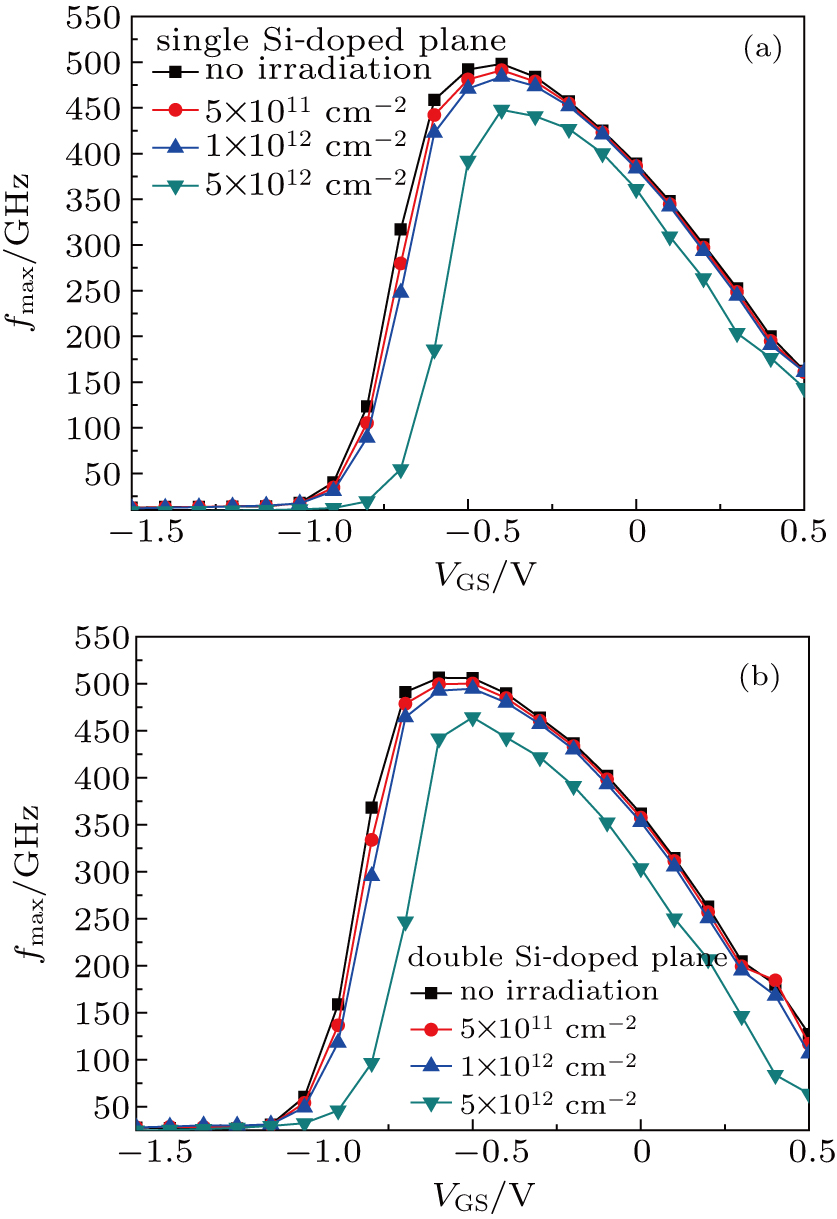
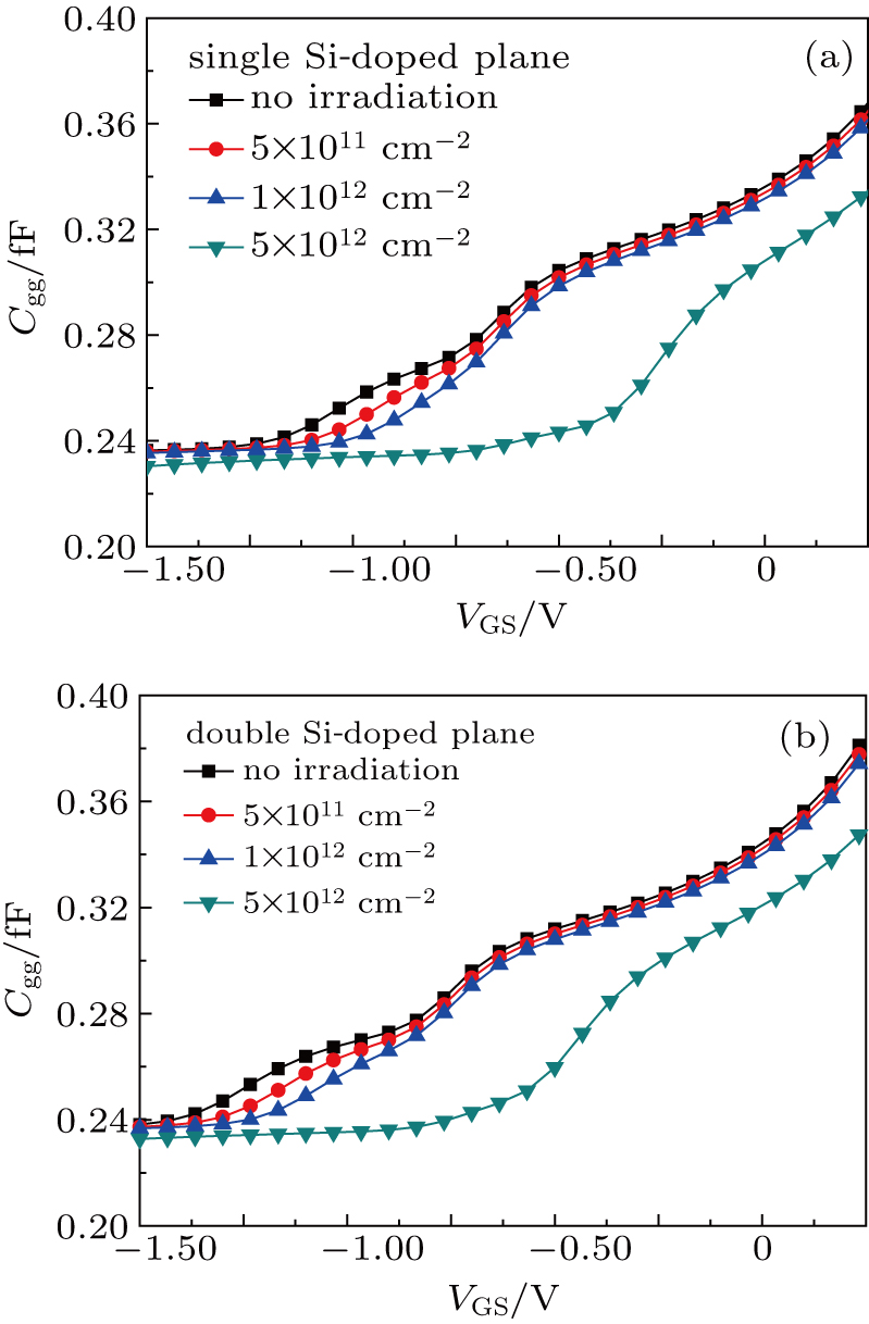
The fT and fmax are vital parameters for high speed device application. Exactly, fmax affects the device power gain of analog circuit, while fT determines the switching speed of digital circuit. Figures
 | Fig. 6. fT of InP-based HEMTs before and after proton irradiations with dose of 5 × 1011 cm−2, 1 × 1012 cm−2, and 5 × 1012 cm−2. (a) Single Si-doped structure; (b) double Si-doped structure. |
 | Fig. 7. fmax of InP-based HEMTs before and after proton irradiations with dose of 5 × 1011 cm−2, 1 × 1012 cm−2, and 5 × 1012 cm−2. (a) Single Si-doped structure; (b) double Si-doped structure. |
 | Fig. 8. Cgg of InP-based HEMTs before and after proton irradiations with dose of 5 × 1011 cm−2, 1 × 1012 cm−2, and 5 × 1012 cm−2. (a) Single Si-doped structure; (b) double Si-doped structure. |
 | Fig. 9. Reduction rates of frequency characteristics for devices with single Si-doped plane and double Si-doped planes: (a) ΔfT; (b) Δfmax. |
The electron concentration in the channel region and their reduction rates are investigated for two kinds of structures before and after 75-keV proton irradiation, as shown in Fig.
In summary, the double Si-doped structure of InP-based HEMT was designed and optimized to improve the proton irradiation tolerance, which eventually has demonstrated superior DC and RF characteristics than traditional single Si-doped structure. Moreover, the inserted another Si-doped plane under channel layer increases the native carrier concentration in channel region, which weakens substantially the carrier removal effect by irradiation-induced defects. Consequently, proton radiation tolerance of double Si-doped structure has been greatly improved with lower reduction rates of DC and RF properties, especially at large irradiation dose. These studies could provide theoretical basis and technical support for irradiation harden design of InP-based HEMTs and integrated circuits, so as to further improve the stability and durability of relative electronic systems.
| [1] | |
| [2] | |
| [3] | |
| [4] | |
| [5] | |
| [6] | |
| [7] | |
| [8] | |
| [9] | |
| [10] | |
| [11] | |
| [12] | |
| [13] | |
| [14] | |
| [15] | |
| [16] | |
| [17] | |
| [18] | |
| [19] | |
| [20] | |
| [21] | |
| [22] | |
| [23] | |
| [24] |


