† Corresponding author. E-mail:
Due to its remarkable electrical and optical properties, graphene continues to receive more and more attention from researchers around the world. An excellent advantage of graphene is the possibility of controlling its charge density, and consequently, the management of its conductivity and dielectric constant, among other parameters. It is noteworthy that the control of these properties enables the obtaining of new optical/electronic devices, which would not exist based on conventional materials. However, to work in this area of science, it is necessary to have a thorough knowledge regarding the electrical/optical properties of graphene. In this review paper, we show these graphene properties very well detailed.
Due to their excellent electrical and optical properties, graphene and other two-dimensioanl metamaterials are attacking tremendous interest from the international scientific community. It is possible to control its charge density, and consequently, the management of its conductivity and dielectric constant, among other parameters. Hence, obtaining new electronic and optoelectronic devices is possible, which would not exist based on the conventional materials. Researchers have already presented many graphene-based optoelectronic devices that would not be developed based on conventional materials, such as transistors, sensors, antennas, switching cells, as well as highly promising solar cells, among many other new devices.
Although in this manuscript we focus on graphene’s photonic and optoelectronic properties, the inserted subjects can serve as the basis for the study of the technology related to nanophotonic devices based on other two-dimensional (2D) metamaterials that are emerging. For example, black phosphorous (BP) is being highly researched, for the same reason that occurs with graphene, i.e., the very promising electronic, photonic, and mechanical properties.[1] There is a huge interest in 2D silicon – silicene (the term silicene was introduced by Gusmán-Verry and Lew Yan Voon in 2007), due to the preservation of silicon use in the electronic/optical industry, as well as the fact that silicon is the second most abundant chemical element in the earth’s crust.[2]
Despite the enormous interest in the use of electromagnetic waves in telecommunications, in the THz frequency range, technologies-based devices related to conventional materials (3D) do not offer conditions to take advantage of this large and important frequency range. On the other hand, materials consisting of one or a few layers of graphene, black phosphorus and transition metal dichalcogenides (TMDs), for example, can be used in optoelectronic devices to operate with electromagnetic waves in this frequency range. It is possible due to their photonic and optoelectronic properties, as well as the possibility of manipulation of the physical parameters inherent to these materials via the application of an external voltage (gate voltage) or chemical doping. In addition, these devices can operate in the modulation-based THz frequency range, nonlinearity, filtering, and plasmonic.[3]
In dense wavelength division multiplexing (DWDM) optical communication networks, the high transmission rate is impaired, because on routers/switches require an optical/electric/optical conversion. Although the fully optical switches already exist for some time, the switching process is poor, since the optical buffers made up of optical delay lines have huge dimensions and difficult operational control. We have obtained a photonic crystal-based optical memory operating similarly to a dynamic random access electronic memory (DRAM).[4] However, we replaced the photonic crystal with graphene, so that we developed a nanophotonic DRAM optical memory with much smaller dimensions and much faster than a DRAM electronic memory, and got its respective patent (INPE/BR 10 2015 029772 6 - 27/11/2015). Besides, due to the nanometric dimensions of the graphene-based devices, we can integrate these referred devices into photonic integrated circuits (PICs), which will replace, with enormous advantages, the current electrical integrated circuits.
It is noteworthy that to work in this area of science, it is necessary to have a thorough knowledge regarding the photonic and optoelectronic properties of graphene. In this review paper, we show the photonic, electrical, and optical properties of graphene in a very well detailed way.
Phonon-plasmon polaritons, exciton-plasmon polaritons and plasmons polaritons are detailed in Section
For a better understanding of the surface plasmon polaritons in graphene (Section
This subject may be extended to other actively researched 2D materials such as hexagonal boron nitride (insulator),[5] phosphorene (direct bandgap semiconductor),[6] silicene, germanene, and stanene (monolayers of silicon, germanium, and tin, respectively, which are also in the so-called carbon group),[7] and transition metal dichalcogenides (DTMs), i.e., MX2 (M is a transition metal and X a chalcogen),[8] which are also very promising 2D materials, for the next generation of electronic and optoelectronic devices.
The term polariton is used to represent the tight coupling of an electromagnetic wave with an excited state having a dipole moment (phonon, exciton, or photon). Briefly, for the longitudinal polaritons, the electric field has a nonzero component in the propagation direction. On the other hand, for the transverse polaritons, the electric field has no component in the propagation direction.
Phonon polaritons were first studied by Kun Huang (1951) when he studied photon coupling with the phonon and named this phenomenon as phonon polariton. Following this, in 1958, Hopfield, after researching photon coupling with exciton, defined this coupling as exciton polariton. The theory involving these two phenomena continues being developed to date (bulk and surface). However, concerning plasmons polaritons in graphene (and in other 2D materials), researchers have focused on surface plasmons polaritons.
Phonon-plasmon polaritons are quasiparticles that result from strong interactions between photons and phonons, which can occur as surface and volume confined waves. The dispersion relation for phonon polaritons is highly dependent on the material. While volume polaritons tend to approach asymptotically to the longitudinal optical phonon frequency of the material, the surface polaritons tend to approach the surface phonon frequency.[9]
One reason for interest in recent research on bulk and surface polaritons is to obtain optoelectronic devices that operate with electromagnetic waves in the THz and mid-infrared (MIR) ranges.[10–12] We will comment on the results of studies on surface plasmon-phonon polaritons (SPPPs) in doped GaAs, which resulted in the emission of radiation in the THz range.[13]
It is noteworthy that SPPPs occur at the interface of two media with dielectric permittivities of different signs. The dispersion relation for SPPPs is given by[14]


Other research has revealed that the electrical permittivity for electron-doped GaAs (n-GaAs), considering the contributions of the lattice, as well as the free electrons, is given by[15]


For the existence of surface plasmon-photon polaritons at the GaAs/vacuum interface, it is necessary that Re(ε1) < 0, and |Re(ε1)| > 1, the curves referring to the real and imaginary parts of ε1 are plotted as a function of the energy of the modes (in meV) present in a GaAs/vacuum plane interface (Fig.
 | Fig. 1. Real (solid line) and imaginary (dashed line) parts of n-GaAs dielectric permittivity (from Ref. [13]). |
It is noteworthy that the following values were considered: the free electron concentration Ne = 2 × 1018 cm−3, and mobility μ = 2500 cm2/V·s. Moreover, as the GaAs conduction band is nonparabolic, the dependencies of μ and γ on the doping level were taken into account,[16,17] as well as the electron concentration dependence on me.[17]
As we can see in Fig
From Eqs. (
 | Fig. 2. (a) SPPP mode energy versus KSPPP, or versus kPh sin θ + mkG for θ = 11° (solid line). (b) Those for normal incidence (adapted from Ref. [13]). |
Notice in Fig.
Figure
The reflectivity that occurs on a flat GaAs/vacuum interface was also investigated, as shown in Fig.
 | Fig. 3. (a) Reflectivity spectrum in a sem-infinite plane interface GaAs/vacuum. (b) Absorptivity spectrum in a sem-infinite plane interface GaAs/vacuum (adapted from Ref. [13]). |
The insertion of a regular grating at the semiconductor surface (for instance, using photolithography technique) may cause changes in the reflectivity spectrum, which may provide the conversion of photons into surface plasmon-phonon polaritons, as well as the conversion of surface plasmon-phonon polaritons into photons. It is noteworthy that the occurrence of such a conversion may lead to the emergence of resonant dips in the reflectivity spectrum.
The reflectivity spectrum points were determined (where these dips exist, i.e., SPPP modes excitation occurs), considering the surface grating period a = 60 μm, as shown in Fig.
Inserting a surface grating can also alter the absorptivity spectrum of GaAs significantly. It is noteworthy that in this case, as the non-equilibrium SPPPs modes can scatter on the surface grating, there may be the occurrence of a transformation of surface plasmon-phonon polaritons into photons. Consequently, this transformation can cause resonant peaks in the absorptivity spectrum, which are shown in Fig.
The incidence of photons on the surface of a solid may lead to the occurrence of electron (in the conduction band)–hole (in the valence band) pairs, i.e., excitons, due to the absorption of photons.[19,20] There are two types of excitons: Wanner[21] and Frenkel.[22] Wanner excitons are generally present in semiconductor materials, have weak coupling interaction and wide distributions of electrons and holes. On the other hand, the Frenkel excitons are usually located in insulating materials, have strong Coulomb interaction, and the electrons and holes are bound in somatic cells. Indeed, the incidence of photons in a two-level system (for example, an atom or ion characterized by a ground state and an excited state) can cause the periodic exchange of energy between the light field and this two-level system. The oscillations arising from the above mentioned process, called Rabi oscillations (named after Nobel Prize laureate Isidor Isaac Rabi), are associated with oscillations of electrons and photons. In other words, these oscillations can be defined as a periodic change between absorption and stimulated emission of photons and can be modeled by the Bloch vector formalism. The angular frequency of the Rabbi oscillations is called the Rabi frequency.
The coupling between photon and exciton (exciton-polariton) can be detailed from Maxwell’s equations so that the equation that determines the dispersion relationship for excitons-polaritons is given by[23]

The dispersion relationship for bulk exciton-plasmon polaritons, related to the GaP, is shown in Fig.
 | Fig. 4. (a) Dispersion relation of bulk exciton-plasmon polariton in ZnO (solid lines). (b) Dispersion relation of surface exciton-plasmon polariton in ZnO (solid line between wT and wL, adapted from Ref. [23]). |
The horizontal dashed line represents the longitudinal resonance frequency, and the dashed-dotted line represents the transverse resonance frequency. Note that there are two branches, upper and lower branches. The longitudinal-transverse splitting, i.e., wLT = wL − wT, represents the possibility of coupling strength between the exciton and photon.
The surface exciton-plasmon polariton is made up of strong coupling between photons and excitons, and these modes have the wave vector component in the surface plane. From Maxwell’s equations, considering the continuity of the electric field at the surface, it is possible to obtain the dispersion relation of the surface exciton-plasmon polaritons according to the equations shown below:


Equations (
It is noteworthy that both phonon-polariton and exciton-polariton have longitudinal-transverse splitting, i.e., longitudinal-transverse symmetry breaking. However, the LT-splitting for exciton-polariton is small. Note that wLT = 008 meV for GaAs,[24] and wLT = 5.00 meV for ZnO so that the dispersion relation for the surface exciton-plasmon polariton is approximately linear. Therefore, the effective mass of exciton-polariton approaches infinity, which means that it can not move, and the states in this band can be neglected.
The interaction between localized surface plasmons (LSPs) and photons may provide some advantages regarding optical properties, such as, a longer lifetime of excitons and a large increase in the quantum yield.[25,26] Taking into account that in metal nanostructures can have an energy of localized EM field, the intensity of the electric field can be increased,[27] and there may be nonlinear effects.[28] To achieve a composite structure with enhanced optical properties, hybrid metal/semiconductor structures are being much researched, because of the interaction between SPs and excitons.[29–31]
The combination of metal and semiconductor constituting a hybrid structure provides optical properties which can be used for the nanometer scale of electromagnetic energy flow control. For example, interactions in hybrid structures can be obtained between quantum-confined electronic states located in the semiconductor and confined electromagnetic modes located in the metal. In other words, exciton-plasmon interactions obtained in this way can provide various effects, such as absorption and emission, control of nanoscale energy-transfer processes, creation of new excitations in the strong coupling regime, and increase of optical nonlinearities.[32]
Surface plasmon polaritons (SPPs) can occur due to the coupling between the oscillations of the electron plasma with photons, which propagate at the interface between a dielectric and a conductor.
To enable the detailing of SSPs in graphene (GSPPs) as well as in other 2D materials, we start from the theory that involves SPPs in metallic interfaces.
From the Maxwell and Helmholtz equations, we can determine the equations that represent the behavior of the metal/dielectric interface SPPs, referring to both sides of this interface, as shown in Fig.
 | Fig. 5. Schematic representation of an electromagnetic wave propagating in the x-direction of a metal/dielectric planar interface. |
The following equations can be used for TM modes:[14]


Recall that a metal (in this case located at z < 0) has a negative real part dielectric function (Re[ε1(w)] < 0) for frequencies below the plasmon frequency (wp), and the dielectric (in this case located at z > 0) has positive dielectric constant ε2.
The continuity condition of Hy ad εiEz at the interface requires that A1 = A2 so that


Getting back to the SPPs TM on metal/dielectric interfaces, we can state that the energy of electric and magnetic fields of SPPs at these interfaces has exponential evanescent decay, as shown in Fig.
We can apply the Drude model by adding the effective parameters wp (plasmon frequency in eV), γbulk (proportional to the reciprocal of the mean free time between electron collisions), and ε0 (contribution of interband transitions to the polarizability)[33] to determine the dielectric function of the metal, as given by

From Eq. (
 | Fig. 7. Real and imaginary parts of the propagation constant of SPPs modes in a gold/silica interface, as a function of the incident photons energy. |
We used Eq. (
In Fig.
Note that we used the energy range between ∼ 0.8 eV (λ = 1.55 μm) and ∼ 4.133 eV (λ = 0.3 μm) for the incident photons, i.e., in the range from infrared to ultraviolet. Interestingly, in this case, the maximum value of the real part for SPP modes is βm ≈ 4.332 × 10⁷ + 3.469 × 10⁷i, the energy of this mode is Eβ m ≈ 2.561 eV, and λβ m ≈ 2π/Re(βm) ≈ 145.05 nm. It is noteworthy that for values greater than Eβ m, the real part of SPPs modes drops dramatically, but from certain energy, the real part of SPPs modes starts to grow again, but less intensely. This means that from this maximum wavenumber value, the value of the wavenumber in the z direction (
Besides, for the occurrence of SPPs at the metal/dielectric interfaces, it is necessary to use an insertion technique to achieve the match for the wave vectors of the SPPs and the incident light. Recall that the imaginary part of the propagation constant represents the energy loss of the SPPs modes, that is, the attenuation of the SPPs modes so that the propagation length and wavelength of SPPs modes are given by

Although the surface plasmons polaritons in metals (SPPs) and in graphene (GSPPs) come from identical processes, their physical characteristics are different. The main reason for this occurrence is because, in graphene, the electrons are practically free in the normal direction to the plane. It is noteworthy that in graphene, electrons behave like massless Dirac fermions, which gives excellent properties, such as charge carriers (electrons and holes) with high mobility and relatively long average propagation length. Moreover, graphene provides the charge density management via gate voltage (or chemical doping), as well as anomalous Hall effects, among many other advantages, compared to noble metals.[36,37]
The aforementioned, combined with the different dispersion relations, provide different TM modes in graphene (compared to what happens in metals), which brings other advantages, such as higher concentrations of fields, electric and magnetic, as well as higher wavelengths ratio from photons in air and surface plasmons polaritons (λair/λGSPP), as well as higher propagation length of GSPPs. Note that this last cited advantage provides much more efficient graphene-guided nanophotonic devices based on guided waves. Besides, in graphene, TE modes can be coupled, unlike noble metals, which are much more expensive than graphene.
We can also cite the fact that due to the physical properties of GSPPs, graphene can enhance photon absorption.[38,39] Incident light can be completely absorbed in nano-disks with graphene matrix structures, depending on the angle of the incident light.[40]
As we will detail in the following sections, the electrical and optical properties of graphene are based on plasmon. We can note that these properties are being increasingly researched, resulting in new and efficient optoelectronic devices. Research has been conducted to investigate the coupling process of radiations emitted by an emitter located above and adjacent (in the same plane) to the plane of a thin graphene film with SPs modes present.[41] Radiations have been polarized in all three dimensions to find out which type of emission is the most efficient. An emitter is located 30 nm above the graphene plane so that the emitted radiation reaches the central part of the plane. When the emitted radiation has polarization in the y-direction, the coupling efficiency between the emitted radiation and the GSPPs rises (greater amount of transmitted energy, i.e., more GSPPs modes are produced). The coupling efficiency for the polarization of the light in the y-direction is greater than that polarized in x and z-directions (z-direction is normal to the graphene plane). On the other hand, when the light emitter is located on the same plane as the graphene film, it is obvious that there is no coupling when the radiation is polarized in the z-direction. Moreover, the coupling efficiency for the x and y-directions is lower than that for the light emitter located above this plane. Hence, unlike metal/dielectric interfaces, where it is necessary to apply a Kretschmann or an Otto configuration to enable the coupling of photons to SPPs, in graphene, photons can be directly coupled to GSPPs.
Hybrid structures based on graphene and other 2D and 3D materials are providing excellent results. A photodetector consisting of a multilayer MoS2 thin film and a thin layer of graphene quantum dots over the MoS2 layer was presented, which has photo responsiveness of approximately 104 A·W−1 and a photo gain of approximately 107 electrons per photon. This phenomenon is caused due to the effective transfer of charge and re-absorption of photons during the photons incidence. Thus, the light–matter interaction is enhanced, causing enhanced light absorption as well as the creation of electron–hole pairs.[42]
In the following sections, we will detail the GSPPs-based electrical and optical properties of graphene.
Even considering the ideal graphene, i.e., without charge density at Dirac point, its conductivity is not null, since graphene has a universal conductivity (for any frequency) with value 
However, it is possible to move the Fermi level (EF) located at the Dirac point up (electrons (n)-doped)) or down (holes (p)-doped)) by applying a gate voltage, or a chemical doping, so that the change in charge density provides the change of the conductivity of graphene.
In the left part of Fig.
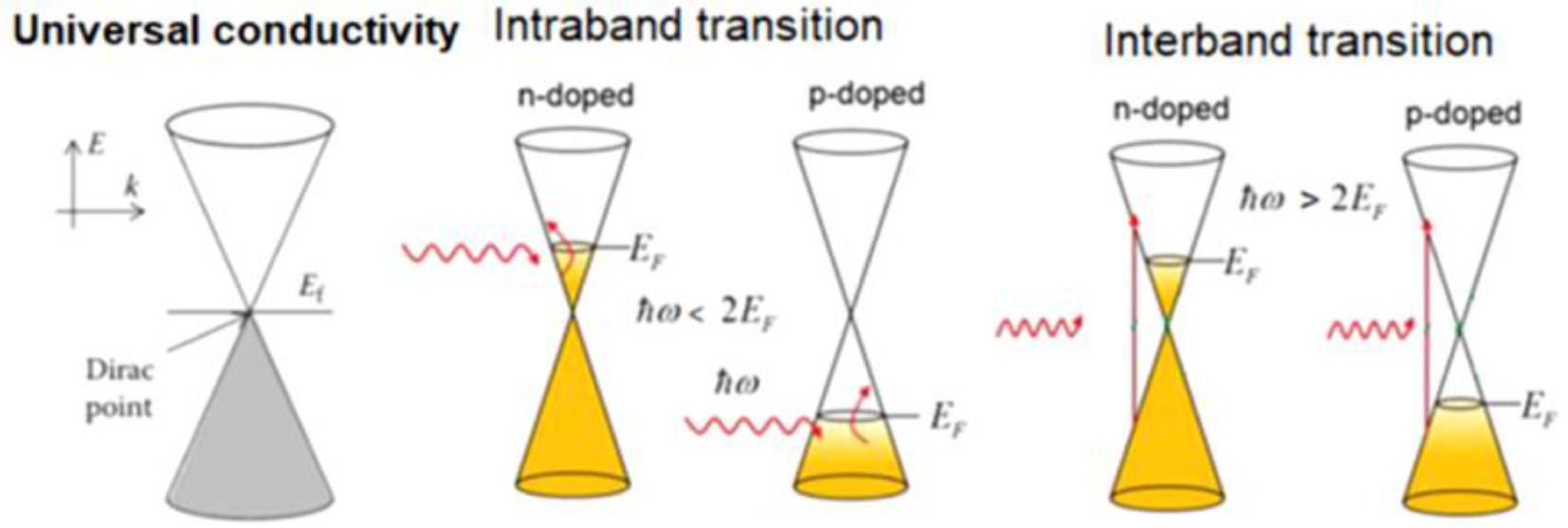 | Fig. 8. Schematic representation of the energy band referring to intrinsic graphene (left part), intraband transition (central part), and interband transition (right part). |
Note in the central and right parts of Fig.
In addition to what we have shown above, to detail graphene conductivity, it is also necessary to show the relationship of the chemical potential (μ) with the Fermi level, as well as the equations that determine the chemical potential, charge density (n), and electron relaxation time (τ) for graphene. Therefore, considering the value of the KBT/μ ratio too small, we can state that[44–47]


To find the graphene conductivity equation, we start from the following equation:[44,48]
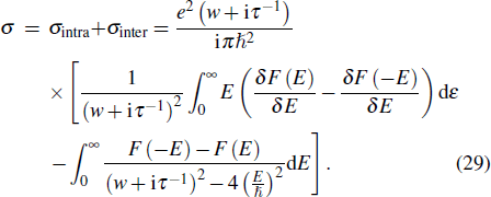
After some mathematical manipulations, we arrive at the mathematical expression that determines the intraband conductivity[44,49]


We also rely on the following equation for the determination of graphene conductivity:[50]

In the above equations, the conductivity values are given as sheet conductivity (with uniform thickness) in Siemens (S). Briefly, to transform sheet conductivity to volume conductivity (S/m), it is necessary to divide the value of the sheet conductivity by the thickness of the film.
Equations (
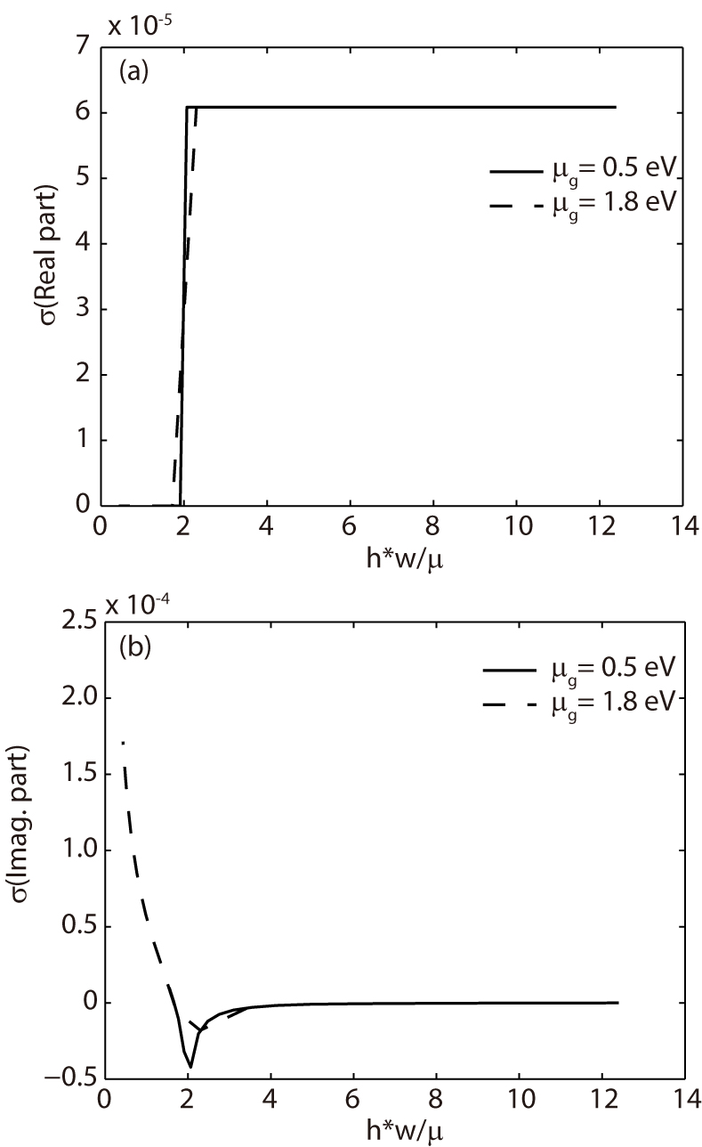 | Fig. 9. (a) Real part and (b) imaginary part of the conductivity for a graphene layer (as a function of Ω). |
We use the value of load mobility in isolated graphene (3.39 × 105 cm2·V−1·s−1).[51] Note at the top of Fig.
It is necessary to block interband transitions, i.e., the first-order process, by increasing the graphene’s chemical potential to avoid the changing in the conductivity. Thus, only GSPPs with a frequency above the limit (ħwinter/μ = 2 → winter = 2μ/ħ) suffer this type of attenuation.
However, it has been proven through research that there is still another mechanism of energy loss of SPPs (including GSPPs), which is caused by the phonon emission (second-order process) and the consequent occurrence of electron–hole pair. It is noteworthy that this second-order process, although often neglected, happens for frequencies above a certain threshold (woph), i.e., w > woph since losses are negligible for frequencies below this threshold. It is important to state that for woph < w < winter optical losses, as the first-order process is avoided, but attenuations still occur due to the second-order process. In these researches, the optical loss values were obtained using the methods random-phase approximation (RPA) and number conserving relaxation-time (RT) for the second-order process.[52]
The general equation that gives the effective relative permittivity (dielectric constant) of isolated graphene is given by[53]

However, for the determination of the effective relative permittivity of graphene, another equation was obtained. In this case, by admitting a volume conductivity as a function of very thin thickness, i.e., Δ → 0 (to recover the two-dimensional geometry of graphene), this equation is given by[54]

Note that in this case, the real part of the graphene’s effective relative permittivity is given by 


Besides, an equation concerning the effective relative permittivity, which takes into account the air impedance (η0 ≈ 377 Ω), photon wavenumber of the vacuum (k0), as well as the 2D graphene conductivity (σ) is given by[45]

The dispersion relationship obtained from Maxwell’s equations for TM modes, considering the dielectric layer embedded in two distinct dielectrics, is given by[45]


We can state that for TE modes using the same reasoning as above, the dispersion relation for graphene embedded in a dielectric medium is given by


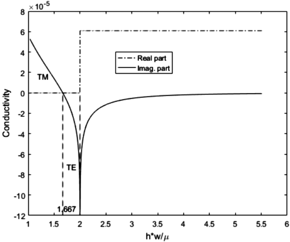
The plot of the imaginary part of graphene conductivity in air calculated by Eqs. (
In Fig.
Note that for ħw/μg > 2, the real part of the graphene conductivity is greater than zero so that the TE modes are attenuated, and there are no TE modes.
It is noteworthy that the increase in temperature causes a slight change in the real part of graphene conductivity around the bifurcation point (where σ′ = 0) so that the real part of conductivity becomes slightly positive for some values of ħw/μg ≈< 2, which results in small attenuations of GSPPs modes. However, TE modes suffer greater attenuation than TM modes.[45]
The schematic representation of a double-layer of graphene, embedded between 3 dielectric media, is shown in Fig.
From the equations that determine the electric fields, applying the boundary conditions on both interfaces, and assuming exponential decay of the fields, we can get the dispersion relation for this device[56]


Assuming all dielectrics are equal, that is, ε1 = ε2 = ε3 = εd and 

On the other hand, according to the conventional waveguide theory, the electric fields in the different regions of the double-layer graphene device (Fig.
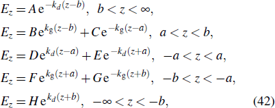


Taking into account the boundary conditions (the transverse electric and magnetic fields are continuous at the interfaces), as well as using the limit for the smallest possible value of the distance d, when d → 0, the dispersion relation of this device is given by


We plot the real parts of the even and odd mode propagation constants using Eq. (
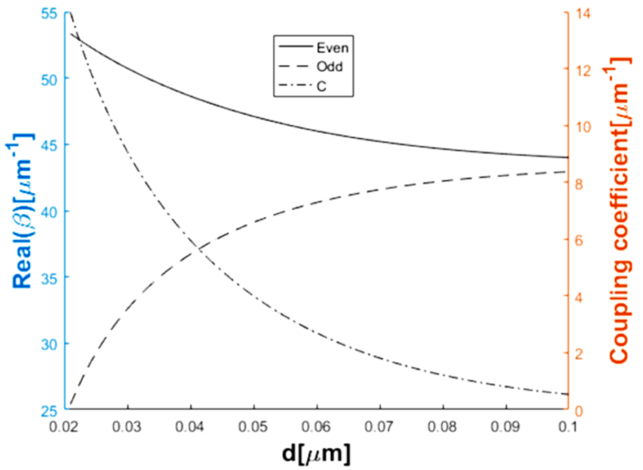 | Fig. 14. Graphs referring to dispersion relations for even and odd modes, and coupling coefficient, according to the parameters presented above. |
The results are identical, and the slight difference between the values may have been caused by the fact that we used the general graphene conductivity equation (σ = σintra + σinter) according to Eqs. (
It is noteworthy that this device can operate as a directional coupler whose coupling coefficient (C) is given by[46]

For comparison, in Fig.
Taking into account a graphene sheet over h-BN, according to Eq. (


It is noteworthy that for the same conditions as above, but using graphene over h-BN, we have λ0/λGSPP ≈ 165 and δGSPP ≈ 1775 μm. Note that the propagation length in graphene over h-BN is approximately 6.673 greater than that in graphene over SiO2.
Figure
Figure
Figure
As we can see (for the conditions mentioned above), the higher the chemical potential, the lower the ratio λGSPP/λ0 and, the higher the λ0, the lower this ratio.
The quality of the substrate on which a graphene sheet is deposited needs to be carefully checked to maintain graphene with good quality. This is very important because to obtain graphene with good quality (after its transfer), the substrate must be free of wrinkles, distortion, and other types of defects. However, the thermal deposition of SiO2 usually causes high surface roughness, and graphene over SiO2 has no homogeneity of charges along its surface.
For comparison, while a SiO2 surface with dimensions 0.5 μm × 0.5 μm has Rpm (average of the highest roughness peaks above the average level in five measurements) = 250, an h-BN surface with the same dimensions has Rpm = 50.[62]
A single layer of h-BN, termed white graphene, is also contained in a plane. This material is a graphene isomorphic, in which the boron and nitrogen atoms are located at points A and B of the same atomic structure presented for graphene so that the atomic structure of h-BN is similar to that of graphene. Note that boron and nitrogen atoms are the closest neighbors to carbon atoms in the periodic table, the number of electrons of two carbons is equal to the sum of the number of electrons of boron and nitrogen.
It is noteworthy that graphene has a unit cell consisting of carbon atoms distanced by 0.142 nm, its atomic lattice has a structure parameter with a value of 0.246 nm. On the other hand, h-BN atoms (boron and nitrogen) are 0.144 nm apart, and its structure parameter has a value of 0.25 nm. Moreover, the space between two layers of graphene is 0.355 nm and the space between two layers of cubic h-BN is 0.333 nm.[63] The value of the dielectric constant of h-BN (between 3 and 4) is close to that of SiO2.[58,59,64,65]
Besides, we have mentioned above, note at the bottom of Fig.
 | Fig. 18. Schematic representation of a system consisting of a graphene layer embedded between two layers of h-BN. |
Despite of the existence of a great similarity of graphene with h-BN, while graphene is considered as a null bandgap semiconductor, h-BN is considered as an insulator, whose bandgap is 5.97 eV.[66] Like graphene, in h-BN, the covalent bonds between boron and nitrogen atoms are composed of sp2 hybrid covalent bonds, which form strong σ bonds in the plane,[67,68] and the layers are supported by weak van der Waals forces. Therefore, both graphene and h-BN have very strong covalent bonds in the plane and weak van der Waals forces between adjacent planes.
Considering that the h-BN roughness is much lower than the SiO2 roughness, graphene embedded between h-BN layers has much higher charge mobility and homogeneity, when compared to embedded between SiO2 layers.
It is noteworthy that the charge mobility of graphene over h-BN has been determined, i.e., μm = 60000 cm2/V·s,[58] which is the value we adopted in our work.
On the other hand, a lot of research has been carried out to determine graphene on SiO2,[69–72] but the value μm = 10000 cm2/V·s is the most widely reported in the international scientific literature. Note that this value is much lower than that of graphene on h-BN.
Since there are very few charge traps on the h-BN surface, graphene on h-BN has a marked improvement on its electronic properties, when compared to on SiO2.[64] Experiments have shown that graphene sheets can withstand electrical current density greater than 108 A/cm2, for widths less than 16 nm. The graphene sheets used in these experiments were produced by exfoliation of graphite through adhesive tapes and adhered to an oxidized silicon substrate with an oxide thickness of 300 nm. The breaking current density is related to the resistivity of the graphene sheet, Joule heating being the most likely breaking mechanism.[73] Therefore, as the resistivity of graphene on SiO2 is higher than that of graphene over h-BN, the breaking current density in graphene over h-BN must be even higher.
In Fig.
As graphene has no prohibited bandgap, the generation of charges due to light absorption occurs over a wide range of wavelengths, including ultraviolet, visible, infrared, and teraHertz ranges, which is not possible by the use of metals. Besides, the transmittance (T) of undoped graphene is independent of the incident photon wavelengths. The T is determined by

On the other hand, a graphene layer has a reflectance of only 0.1% of the incident light. However, for a graphene film constituted by ten layers, this value increases to 2%.[51] Therefore, we can state that a graphene layer has absorbance A = 1 − T ≈ 2.3%.
Two-dimensional materials such as graphene and MoS2 have an absorption coefficient > 5 × 10⁷ m−1 in the visible light frequency range, which is ten times higher than that of GaAs and Si.[15] Due to its very thin thickness, the absolute value of graphene absorbance is very small. However, the absorbance of some overlapping layers is approximately proportional to the number of these graphene layers.[50–52] On the other hand, this absorbance loses the proportionality mentioned above when it comes to significant graphene layer numbers, but the transmittance remains high. For example, graphene with overlapping layers providing 1 μm thickness has a transmittance of approximately 70%.
The absorption spectrum of a graphene layer is quite flat (between 300 nm and 2500 nm), but there is an absorption peak in the ultraviolet region (≈ 270 nm).[53]
Indeed, absorbance, reflectance, and transmittance depend on some factors, such as materials used above and below the graphene layer, angle of incidence, and type of light polarization. Although we are focusing on graphene, this theory can serve as the base to other 2D group IV materials (silicene, germanene, and tinene).
Graphene embedded in two media (j = 1, 2), can be characterized by the dielectric functions (or refractive index) of these media. Moreover, the conductivity of graphene defines its effective dielectric constant, which can be complex. We will use the normalized conductivity of graphene (
Let us consider the dielectric functions and the refractive indices of the two media involving the graphene layer, given by

In Fig.
 | Fig. 19. Light propagating through dielectric graphene junctions, where graphene is embedded in two dielectric media, which have real refractive indices. |
However, assuming that the refractive indices of the two media are complex, we have[50,74,75]


It is noteworthy that considering the dielectric medium 1 with real refractive index (with null extinction coefficient), the incidence angle (θ1) is real and the refractive angle (θ2) is given by

Note that the refractive angle can be complex. Considering the medium 2 as absorbent, we have the transmittance, reflectance, and absorbance given by[41–43]


Note that in this case, the transmittance and reflectance values for TM and TE modes are about the same. According to that has already been detailed previously, the TM and TE modes do not suffer attenuation (photon absorption).
At the bottom of Fig.
For the same structure mentioned above, we obtained the wavelength absorbance graphs (0.3 μm ≤ λ ≤ 1.6 μm), for μ = 0.00 eV, 0.50 eV, 1.00 eV, and 1.50 eV, considering the normal incidence angle at the surface, as shown in Fig.
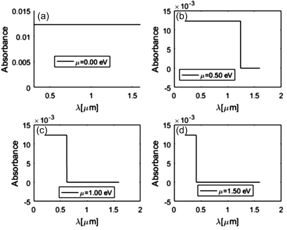 | Fig. 21. The absorbances referring to the structure consisting of h-BN/graphene/h-BN as a function of λ, for μ = 0.00 eV, 0. 50 eV, 1.00 eV, and 1.5 eV. |
Note that for μ = 0, all wavelengths are absorbed (universal) since the conductivity is universal. However, for μ ≠ 0, from the wavelength that provides Ω < 2, the absorbance value is null. Note that for wavelengths in the range of approximately 0.30 μm to 0.50 μm, photon absorption occurs even at μ = 1.5 eV.
Let us now consider an example of a structure air/graphene/silicon for Schottky junction solar cells. We plot the absorbance and transmittance as a function of the incidence angle for TE and TM modes, considering μ = 0, using Eqs. (
We can conclude that while the transmittance and the absorbance for TE modes decrease as a function of the incidence angle increment, for TM modes, the opposite occurs, with a peak value around the angle 0.45 π rad.
In addition to Eq. (


The electrical and optical properties of graphene and other 2D materials are utilized to provide high-efficiency optoelectronic devices that could not be achieved using conventional 3D materials.[76–86] For example, a photo-electrochemical photodetector based on liquid exfoliated lew-layered InSe nanosheets with enhanced stability was presented, taking advantage of the bandgap provided by few 2D-layered materials. The choice of few-layered InSe nanosheets has been determined because of their direct bandgap, excellent transport properties, photoresponse, and simplicity of obtaining (using the liquid-phase exfoliation approach). This photodetector has the advantages of enhanced photocurrent density, responsivity, and cycling stability in KOH solution when subjected to solar irradiation. Moreover, the detection of this photoelectrochemical photodetector can be managed by varying the concentration of KOH and applied potential. Therefore, the physical properties of this device provide a high efficiency of photodetection. Besides, the process of the photodetection, InSe nanosheets can be used in other devices such as dye-sensitized solar cells, water splitting systems, and solar tracking equipments.[87]
Using chemical doping in graphene, it is possible to change the Fermi level, and consequently, the work function. Hence the replacement of metal by graphene in Schottky junction-based solar cells provides enormous advantages and much higher power conversion energy (PCE) regarding metal/silicon interface.
Methodologies for obtaining doped graphene with arsenic and phosphorus have been presented using metal-organic chemical vapor deposition (MOCVD). As a result, it has been found that the value of the phosphor and arsenic doped graphene work function, increased from 4.5 eV (undoped graphene) to 4.7 eV and 4.8 eV, for phosphor and arsenic, respectively.[88]
Other research has shown that the solar cell consisting of graphene/n-silicon Schottky junction, using change in the back contact structure, has a simpler manufacturing process, lower manufacturing cost, and a larger contact area than other graphene/silicon-based solar cells. To increase the PCE value for these solar cells, the poly(methyl methacrylate) (PMMA) residues left in the graphene during the transfer process were removed as much as possible. Due to this cleaning and doping process of graphene, this solar cell presented a PCE value of 14.1%.[89]
It is expected that the size-tunable photon absorption and efficient generation of multiple electron-hole pairs will provide high PCE value for inorganic quantum dot (QD) solar cells (greater than the Shockley–Queisser limit).[90] However, this type of solar cell has poor electron–hole separation and poor transfer of photogenerated electrons to electrodes. The use of graphene as an electron acceptor in this type of solar cell with the multilayered graphene/QD resulted in an incident photon-to-carrier conversion efficiency (IPCE) of around 16% and a photoresponse of 10.8 A/m2 under 1000 W/m2 illumination.[91]
Due to the graphene’s high transparency, up to four layers of graphene enable the replacement of indium tin oxide (ITO) with graphene, for example, in an organic photovoltaic cell (OPV) as a transparent anode, with comparable performance. Research on organic solar cells has revealed that four graphene layers provided the same sheet resistance (30 Ω per square) of the ITO when they were used as the electrode. Hence, the solar cell using graphene replacing the ITO has presented at least 92% of the efficiency regarding the OPV with an ITO electrode for both normal and angular AM1.5 G illumination.[92]
Perovskite metasurface is a new methodology that can be used to increase the efficiency of photonic devices. Research on photonic interactions involving perovskite layer and an interlayer of photoactive organic material in hybrid perovskites has been carried out in order to enable the obtaining of novel photonic devices, such as, photodetectors, solar cells, light-emitting diodes, nanolasers, displays, waveguides, modulators, and nonlinear optical devices.[93]
Gate voltage means applying a voltage between an external medium and a single graphene sheet, between two parallel graphene tapes, or between an external medium and one of the parallel sheets, depending on the geometry of the nanophotonic device which is analyzed. Through the gate voltage, it is possible to control the chemical potential of graphene, which can operate in the conduction or valence band, depending on the applied voltage, due to the diffusion of negative (positive) charges in the graphene plasmonic system (electric field effect).[94]
In Fig.
This type of gate voltage, called back gate voltage, can be used in graphene-based nanophotonic devices, such as a transistor, whose schematic representation is shown in Fig.
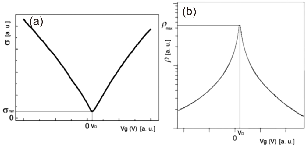 | Fig. 24. (a) Example of conductivity versus gate voltage for a graphene channel transistor. (b) Example of resistivity versus gate voltage. |
The conductivity of graphene increases (while obviously, the resistivity decreases) as the absolute value of the back gate voltage increases, regardless of whether the voltage applied to the highly doped silicon is positive (and negative in graphene, causing electron transfer to graphene) or negative (and positive in graphene, causing the transfer of holes to graphene).
The position of the Fermi level, whose value is practically the same as the chemical potential of graphene, is controlled in this case by the back gate voltage Vbg. It is noteworthy that considering graphene as ideal, for Vbg = 0 eV graphene would have the minimum conductivity (σmin). However, considering real graphene, the minimum conductivity does not occur under this condition, given the unwanted doping of the graphene from the environment and the device manufacturing process, among other factors.
The Dirac voltage (VD), i.e., the gate voltage where the minimum conductivity (or maximum resistivity), for example, in graphene on SiO2 occurs, has been studied in several experiments, where the influence of the manufacturing and cleaning process of graphene was verified. Additionally, at the interface, there are energy states that behave as charge acceptors or donors. Therefore, there are different values for the graphene Dirac voltage.[96–100] It is noteworthy that the residual charge density in graphene n0 has typical values between ∼ 5 × 1010 cm−2 to ∼ 30 × 1010 cm−2 (p-type doping), for graphene on SiO2/Si depending on the charge impurity density in SiO2.[101] So, even without gate voltage, graphene has a residual charge density and for this reason, it is necessary to exclude this charge density from the value of the charge density provided by the gate voltage as shown in Eq. (
In the case of back gate voltage, considering graphene and highly doped silicon surface, such as the plates of a flat capacitor and SiO2 as the dielectric between the plates, the density of graphene charge carriers due to the application of Vbg is given by

On the other hand, the graphene conductivity can be, theoretically, determined from a semiclassic diffusive transport model according to the following equation:

Considering that practically all potential difference occurs in the dielectric medium, which in a back gate structure has a large thickness, a large potential difference (ddp) is needed to obtain moderate increments of charge density. However, the application of high values (ddp > 100 V) causes the damage of SiO2. Therefore, as we have mentioned above, we can state that the back gate voltage process is limited. To overcome this problem, it is necessary to decrease the thickness of the SiO2 layer, but obtaining thinner layers of this dielectric to support the graphene layer requires more advanced techniques. Another solution is to use a medium with high dielectric constant, such as HfO2. Thus, the most used solution is the application of a top gate voltage on graphene, so that the dielectric has a small thickness.
One option for improving the top gate voltage efficiency is to replace SiO2 with h-BN, the thickness of the h-BN layer being thin enough (usually between 10 nm and 20 nm), to increase the efficiency of charge generation in graphene. Figure
In the top gate voltage structure, a graphene sheet shall be deposited on the silicon, and the insulator shall be deposited above the graphene so that the insulator is in contact with the gate electrode. Since in this case, the dielectric thickness is small (generally 5 nm to 15 nm), the quantum capacitance per unit area cannot be neglected. As the quantum capacitance (Cq) is inherent to the graphene layer, we should consider the total capacitance per unit area of the structure (Ct) shown in Fig.


An even more efficient system for applying gate voltage is the simultaneous use of a back gate voltage and a top gate voltage, according to the schematic representation shown in Fig.
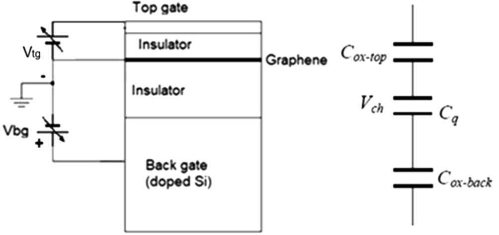 | Fig. 26. Schematic representation of the application of a top gate voltage simultaneously with the application of a back gate voltage. |
Top gate + back gate experiments were performed using a MOSFET where a graphene film was used as the channel of this transistor (length = 5 μm, width = 1 μm). The graphene film has been grown in metal and transferred to a SiO2 layer, which was located on a silicon substrate. The dielectric used in the top gate was HfO2 (εdt = 16) and in the back gate was SiO2 (εdb = 3.9).[105]
The charge density on the graphene channel (Qsh) has been determined by the hole and electron density difference, multiplied by the elementary charge value.[106] Hence, the capacitance has been obtained by the Qsh derivative concerning the graphene potential, i.e., Cq = − dQsh/dVch, where Vch = EF/e.
In these studies, it has been found that the minimum quantum capacity at room temperature had a value Cqmin ≈ 0. 8 μ F·cm−2, without taking into account the intrinsic charge density of graphene. However, considering, for example, n0 = 4 × 1011 cm−2 and Vtg = 0 V, it has been obtained that Cqmin = 1732 μF·cm−2.[105]
Note that the total capacity (Ct2) per unit area for the double gate voltage device, shown in Fig.

Another research used a transistor operating with top gate and back gate together consisting of graphene over Si/insulator, in which the source and drain electrodes (left part of Fig.
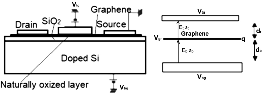 | Fig. 27. (a) Schematic representation of a transistor having top gate + back gate. (b) Electric fields and potentials related to the top gate + back gate system of a graphene channel transistor. |
Between these two electrodes, a 30 nm thick aluminum film was inserted, which was directly deposited on the graphene layer and was used as the top gate electrode. It is noteworthy that the insulation between the aluminum film (top electrode) and the graphene layer was not achieved by the introduction of a conventional insulating film. This isolation was achieved simply after this device remained exposed to the air for a few hours.[108] It was shown that the resistance between the top gate electrode and the source and drain electrodes exceeded 100 MΩ, but the interior of the aluminum electrode remained intact and conductive.
The greater possibility of the occurrence of this insulation film (obtained between the aluminum film and the graphene layer) with an estimated thickness between 5 nm and 9 nm is due to the oxygen diffusion present in the atmosphere, and to the very weak physical contact between the aluminum electrode and graphene layer.[109–111]
In Fig.


The graphene’s Fermi level (approximately the same value as graphene’s chemical potential) is related to the voltage applied to graphene (back voltage) according to the following equation:[112]

Note that for ideal graphene, the gate voltage at which graphene’s maximum resistivity occurs is Vg = VD = 0. In an experiment, it was shown that via the dry transfer of graphene films to the standardized substrate (SiO2/Si), as well as subsequently modified RCA cleaning, devices with low graphene Dirac voltages were obtained, i.e., VD < 4.5 V, with a mean value around 2.5 eV.[113] However, during the investigation of a low flicker frequency in a graphene layer on h-BN/SiO2/Si as well as on SiO2/Si, it was found that VD ≈ 5 V for graphene on h-BN/SiO2/Si and VD ≈ 25 V for graphene over SiO2/Si.[114]
Given the importance of this subject, we will detail the research conducted on gate voltage in a graphene structure over h-BN, which is supported by Cu(111).[115] In this research, the electrostatic doping of graphene, as a function of the applied voltage and the thickness of the h-BN layer, was detailed, using first-principles density-functional theory calculations (DST). It has been observed that even without a gate voltage there is a spontaneous charge transfer between Cu (111) and graphene through h-BN so that graphene maintains intrinsic doping. This charge transfer occurs due to the difference between the work functions of Cu(111) and graphene, but it is strongly altered by displacement of the charges due to the poor chemical interactions at the metal/h-BN interfaces, and h-BN/graphene. However, the application of a variable gate voltage can be used to provide the controlled level of the graphene doping, as it has been shown through other research, where it has been showed that the graphene Fermi level is dependent on the square root of the voltage.[64,116–119]
The structure used in this research has been modeled in a periodic supercell in the normal direction to the plane of the graphene layer (z), with six atomic layers of copper atoms in the surface orientation (111), a thin film with 1 to 6 layers of h-BN, a single graphene layer, and a vacuum region of 15 Å. It has been shown that in this structure (Cu (111)/h-BN/graphene), graphene has intrinsic n-type (electrons) doping. However, the difference between the Fermi level of this structure and that of the graphene decreases with an increasing number of h-BN layers. This intrinsic doping of graphene originates from the transfer of electrons from copper to graphene via h-BN. The working functions related to copper and graphene, without applying a gate voltage, presented the values WM = 5.25 eV and WG = 4.48 eV, respectively. Therefore, in a structure consisting only of copper and graphene, there is an electron transfer from graphene to copper (average electron energy level in graphene is higher than that in copper), so that in this case, graphene is intrinsically positively doped, i.e., the difference in the graphene Fermi level is positive (ΔEF > 0). However, a great influence of the h-BN layer has been proven, because, in the aforementioned structure, this does not occur. Incidentally, in the Cu(111)/h-BN/graphene structure, the difference between the copper and graphene Fermi levels is ΔEFCG = −0.49 eV (average electron energy level in copper is higher than that in graphene), which means that in this case, in order to achieve equilibrium, it is necessary to transfer electrons from copper to graphene so that graphene receives an intrinsic n-type doping.
The explanation for the above can be seen in Fig.
The energy difference between the two interface media is explained by the formation of dipoles between the two materials (at the interface), which occurs due to the Pauli exchange repulsion principle. In other words, this means that the adsorbed charges on the surface cause repulsions concerning substrate charges so that, in this case, electrons transfer to copper occur.[71,120] It is noteworthy that the intensity of these dipoles does not depend on the number of layers of h-BN, for the number of layers greater than 1.[115] In Fig.
 | Fig. 29. (a) Fermi level variance as a function of the applied external voltage (−2 V ≤ V ≤ 2 V), referring to the MG structure. (b) That for the MIG structure. |
Note that the difference between copper and graphene Fermi levels is given by ΔEFMG = WM − ΔEpMH − ΔEpHG − WG. Then, due to charge transfer, a potential difference occurs between copper and graphene so that the h-BN layer is crossed by an electric field, which provides the polarization of the h-BN layer.
On the other hand, by applying a positive gate voltage between copper and graphene, so that an electric field is generated, which opposes the intrinsic electric field mentioned above, it is possible to alter the doping of graphene and consequently its Fermi level. Incidentally, the application of a gate voltage that provides an electric field Eg = 0, 1 V/Å (contrary to the intrinsic electric field) causes a null electric field in the h-BN layers, so that h-BN behaves as if it were isolated. Obviously, the application of an electric field due to a negative gate voltage causes an increase in the polarization of the h-BN layers. Therefore, the application of gate voltage provides the control of graphene doping, and consequently, its Fermi level.
Through further research, an analytical model has been developed for current tunneling and contact resistivity in a metal/insulating/graphene (MIG) structure using gate voltage, where the metal/graphene (MG) junction can be considered as a particular case of the MIG structure.[121] In this model, a voltage drop has been considered between the insulation edges, i.e., between metal and graphene (ΔV). The reason for this voltage drop across the insulator is the difference between the work functions of graphene (Wg) and metal (Wm), so that a charge transfer between these two materials occurs. Moreover, there is also the influence of chemical interactions between graphene and metal.[122]
The displacement of the graphene Fermi level (EFg) concerning the energy level at the Dirac point (ED) as a function of the graphene charge doping is defined as ΔEFg = ED − EFg. In these researches, the relationship between the applied voltage (V) and ΔEFg is presented as

The energy level at the Dirac point (ED = eVD) can be determined by the following equation:


Although equation (
In Fig.
We also plot this same graph for d = 50 nm (not shown in Fig.
The possibility of applying a gate voltage to graphene and other 2D materials is perhaps the most important property of these materials. According to we have detailed in this section, it is possible to change the charge density in graphene by a gate voltage, so that a change occurs in its Fermi level[123,124] and consequently in its work function and conductivity. So, managing graphene’s work function has many benefits that are not possible to achieve using conventional 3D materials. For example, changing the Fermi level makes it possible to use graphene in increasingly efficient optoelectronic devices such as photodetectors and solar cells. On the other hand, changing the controlled conductivity of the graphene via gate voltage causes the change of its effective dielectric constant so that much more efficient optoelectronic devices, such as waveguides, modulators, and full optical switching cells, among many others, can be obtained. We close this review paper, showing the progress and challenges of tuning concerning the electrical and optical properties of graphene via gate voltage.
For some time now, graphene-based transistors have been researched using back, top, or back and top gate voltage, from low frequencies to infrared.[101,125,126] The gate voltage applied to graphene, operating as the channel in a transistor, changes its Fermi level to the conduction (or valence) band so that its conductivity increases with the addition of electrons (or holes) caused by the application of the gate voltage. Hence, it is possible to control the current flowing between the source and the drain electrodes. It is noteworthy that the gate port, i.e., where we apply the gate voltage, the source and the drain ports are located over graphene.
More recent research has presented a logic inverter based on a transistor consisting of p-doped graphene associated with a transistor made up n-doped graphene. Graphene doping was obtained through lanthanide dopants, and the operation of this device is based on C-H-π interactions between graphene and lanthanide dopants.[127] This research may lead to the development of new technologies based on interactions of graphene and other 2D materials with aggregates of molecules, or ions, (supermolecules) joined by noncovalent interactions.
Advances in technology regarding fully optical networks depend on obtaining optoelectronic devices which can be integrated into photonic integrated circuits (PICs). A graphene-based nanophotonic Mach–Zehnder interferometer (MZI) has been introduced to work as a signal follower, switch, splitter, and as a multiplexer/demultiplexer, with dimensions that allow integration into PICs. This MZI consists of an input coupler, two waveguides in the middle (one waveguide longer than the other, so that the modes propagating within the MZI undergo a relative phase shift), and an output coupler. As in graphene-based nanoribbon waveguides, it is possible to insert 90° bends we can reach the difference between the lengths of the two waveguides by inserting a bend in one of these waveguides. However, as the bend is very small and made up of two bends (to allow the same direction), changes were made in its shape to avoid attenuations in the propagating optical signal. Apart from the difference in waveguide lengths, the operation of this device is based on the application of a gate voltage, in order to shift the conductivity and the effective dielectric constant of graphene so that it enables the operation of this device as any of the options shown above. It is noteworthy that the input and output couplers have lengths of 80 nm, and the distance between the two graphene nanoribbons is 2 nm. The difference between the lengths of the two arms has values between 3 nm and 6 nm, which are controlled by the number of carbon atoms located in the propagation direction.[128]
| [1] | |
| [2] | |
| [3] | |
| [4] | |
| [5] | |
| [6] | |
| [7] | |
| [8] | |
| [9] | |
| [10] | |
| [11] | |
| [12] | |
| [13] | |
| [14] | |
| [15] | |
| [16] | |
| [17] | |
| [18] | |
| [19] | |
| [20] | |
| [21] | |
| [22] | |
| [23] | |
| [24] | |
| [25] | |
| [26] | |
| [27] | |
| [28] | |
| [29] | |
| [30] | |
| [31] | |
| [32] | |
| [33] | |
| [34] | |
| [35] | |
| [36] | |
| [37] | |
| [38] | |
| [39] | |
| [40] | |
| [41] | |
| [42] | |
| [43] | |
| [44] | |
| [45] | |
| [46] | |
| [47] | |
| [48] | |
| [49] | |
| [50] | |
| [51] | |
| [52] | |
| [53] | |
| [54] | |
| [55] | |
| [56] | |
| [57] | |
| [58] | |
| [59] | |
| [60] | |
| [61] | |
| [62] | |
| [63] | |
| [64] | |
| [65] | |
| [66] | |
| [67] | |
| [68] | |
| [69] | |
| [70] | |
| [71] | |
| [72] | |
| [73] | |
| [74] | |
| [75] | |
| [76] | |
| [77] | |
| [78] | |
| [79] | |
| [80] | |
| [81] | |
| [82] | |
| [83] | |
| [84] | |
| [85] | |
| [86] | |
| [87] | |
| [88] | |
| [89] | |
| [90] | |
| [91] | |
| [92] | |
| [93] | |
| [94] | |
| [95] | |
| [96] | |
| [97] | |
| [98] | |
| [99] | |
| [100] | |
| [101] | |
| [102] | |
| [103] | |
| [104] | |
| [105] | |
| [106] | |
| [107] | |
| [108] | |
| [109] | |
| [110] | |
| [111] | |
| [112] | |
| [113] | |
| [114] | |
| [115] | |
| [116] | |
| [117] | |
| [118] | |
| [119] | |
| [120] | |
| [121] | |
| [122] | |
| [123] | |
| [124] | |
| [125] | |
| [126] | |
| [127] | |
| [128] |


