Wu Yiqing, Tao Ke, Jiang Shuai, Jia Rui, Huang Ye. Surface passivation in n-type silicon and its application in silicon drift detector. Chinese Physics B, 2020, 29(3): 037702
Permissions
Surface passivation in n-type silicon and its application in silicon drift detector
Project supported by the National Natural Science Foundation of China (Grant Nos. 51602340, 51702355, and 61674167), the Natural Science Foundation of Beijing Municipality of China (Grant No. 4192064), the National Key Research Program of China (Grant Nos. 2018YFB1500500 and 2018YFB1500200), and the JKW Project of China (Grant No. 31512060106).
Abstract
Based on the surface passivation of n-type silicon in a silicon drift detector (SDD), we propose a new passivation structure of SiO2/Al2O3/SiO2 passivation stacks. Since the SiO2 formed by the nitric-acid-oxidation-of-silicon (NAOS) method has good compactness and simple process, the first layer film is formed by the NAOS method. The Al2O3 film is also introduced into the passivation stacks owing to exceptional advantages such as good interface characteristic and simple process. In addition, for requirements of thickness and deposition temperature, the third layer of the SiO2 film is deposited by plasma enhanced chemical vapor deposition (PECVD). The deposition of the SiO2 film by PECVD is a low-temperature process and has a high deposition rate, which causes little damage to the device and makes the SiO2 film very suitable for serving as the third passivation layer. The passivation approach of stacks can saturate dangling bonds at the interface between stacks and the silicon substrate, and provide positive charge to optimize the field passivation of the n-type substrate. The passivation method ultimately achieves a good combination of chemical and field passivations. Experimental results show that with the passivation structure of SiO2/Al2O3/SiO2, the final minority carrier lifetime reaches 5223 μs at injection of 5×1015 cm−3. When it is applied to the passivation of SDD, the leakage current is reduced to the order of nA.
With the rapid development of semiconductor devices, Gatti and Rehak first proposed a new type of nuclear radiation detector, i.e., silicon drift detector (SDD), in 1983.[1] The detector has been widely used in some fields such as space exploration, high energy nuclear physics, and nuclear medicine.[2,3] As the resolution accuracy requirements for SDDs increase, how to reduce the noise of devices plays an important role in the manufacturing process. The noise is mainly determined by the leakage current of SDDs, one of the solutions is to optimize the surface passivation to decrease the surface leakage current. This article is focused on how to optimize the surface passivation of an SDD to reduce its leakage current. There are two main ways for surface passivation of semiconductor devices: chemical and field passivation. Both solutions can be achieved by thin film passivation. The common passivation films are mainly SiO2, Al2O3, etc.[4–8] Since SiO2 passivation films have been put forward, they have been widely used to passivate semiconductor devices. However, high temperature (>1000 °C) to fabricate SiO2 films will cause serious degradation of the silicon substrate. Therefore, plasma-enhanced chemical vapor deposition CVD (PECVD), which features a low-temperature process, has attracted a great deal of attention.[9–13] However, SiO2 films deposited by PECVD are not suitable for surface passivation due to their poor interface and bulk properties, although their deposition speed is very fast. On the contrary, Al2O3 thin films exhibit good passivation property for silicon substrates due to their high atomic hydrogen concentrations.[14–16] However, many experiments have shown that the accumulation of H at the interface during the high-temperature annealing process after deposition of Al2O3 films may cause blistering on the surface, which not only destroys the passivation quality but also increases the leakage current of the device.[17–19] Studies have observed that the blistering phenomenon can be suppressed when a thin SiO2 film is grown between Si-Al2O3 since H has a large diffusion coefficient in SiO2 films.[20–22] Hence, a very thin SiO2 film prepared by the nitric acid oxidation of silicon (NAOS) method is adopted. The NAOS SiO2 film has a compact structure, and is proved to be a good material for surface passivation.[23,24] However, its thickness and deposition rate are limited. In order to achieve high insulation property, a certain thickness of the SiO2 film is needed. Therefore, SiO2/Al2O3/SiO2 stacks is designed to satisfy both the requirements of good interface characteristics and the thickness. At present, such a complex dielectric layer has never been studied in SDD fabrication.
Based on the principles of chemical and field passivation, a new passivation structure, SiO2/Al2O3/SiO2 stacks, is proposed in this paper. The first SiO2 film is formed by the NAOS method because of its low interface state and high density of atomic structure. The second SiO2 film is deposited by PECVD considering fast growth rate at low temperature. A thin Al2O3 film deposited by atomic layer deposition (ALD) is introduced into the two SiO2 stacks to improve the surface passivation. Through the capacitance–voltage (C–V) measurements, it is found that the last fixed charge property in the passivation stacks is the positive charge, which acts as field passivation for the n-type substrate. SiO2/Al2O3/SiO2 stacks fully exploits the advantages of chemical passivation. The passivation structure finally achieves a minority carrier lifetime of 5223 μs at an injection level of 5×1015 cm−3.
2. Experiment
Czochralski-grown 350-μm-thick n-type Si wafers in (100) crystallographic direction, with a resistivity of 3.5 kΩ⋅cm, were used for the passivation experiment. The main process flow is schematically shown in Fig. 1. Firstly, the standard RCA cleaning was performed before passivation to remove saw damage from their surfaces, and then immersed in an HF solution with a ratio of 1 : 100 to remove the native SiO2 layer. Secondly, a thin SiO2 film was formed on the substrate by the NAOS method. Thirdly, an Al2O3 film was deposited by a thermal-ALD system, trimethylaluminum (TMA) and water were used as the reaction source. Finally, a thick SiO2 film was deposited on the Al2O3 film by PECVD at 290 °C and then a short forming gas annealing was performed to activate the passivation layer. It should be noted that all the oxide layers were deposited on both sides of the silicon wafer as shown in Fig. 1. In each step, Sinton instruments were used to record the change of minority carrier lifetime for the samples. The thickness of each oxide layer was measured by an llipsometry (ES) and/or a scanning electron microscope (SEM). The surface morphology of the passivating samples was measured by an optical microscope.
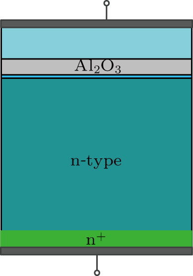
In order to further investigate the fixed charge in the passivation stacks, an MIS structure was designed (as shown in Fig. 2) and C–V curves were measured by a Model 4200-SCS system. At the frequency of 1 MHz, by applying different bias voltages across the electrodes and performing voltage scanning, the MIS structure undergoes three stages of accumulation, depletion, and inversion. By observing the shift of the flatband voltage, the change of fixed charge can be observed. The flatband capacitance is calculated by
where CFB and Cs is the flatband capacitance and the SiO2/Al2O3/SiO2 stacks capacitance, respectively; Cs is the high-frequency capacitance when the device is biased for strong accumulation; εS is the permittivity of the substrate material; and A is the area tested. Here λ is extrinsic Debye length expressed as follows:
where kT is the thermal energy at room temperature (293 K) (4.046 × 10⁻²¹ J), q is the electron charge (1.60219 × 10⁻¹⁹ C), and N = ND/0.9.
We applied SiO2/Al2O3/SiO2 stacks to the manufacturing of the SDD, the main steps are shown in Fig. 3, which has been reported by us in Ref. [25] and the final test structure of the SDD is shown in Fig. 4.
Fig. 3. Schematic of the process flow for the fabrication of the voltage dividers, drift rings, guard rings and entrance windows in silicon drift detectors.
According to the SE results, a thin SiO2 film with a thickness of about 1.2 nm was obtained by the NAOS method. At the beginning, the ALD reaction time was set to 50 cycles, and an about 5.5-nm-thick Al2O3 film was obtained. The thickness of the PECVD-SiO2 film was varied from 300 nm to 600 nm. Figure 5 shows the effective minority carrier lifetime of samples at different structures with or without annealing. The influence of the PECVD-SiO2 film thickness on the passivation lifetime was also described in Fig. 5. When the passivation layer is only a thin SiO2 film obtained by the NAOS method, it is too thin to provide sufficient O to saturate the dangling bond, which results in a low minority carrier lifetime. When the Al2O3 film is grown on the SiO2 film, the lifetime of the minority carrier is improved, whereas the improvement is not great. When the SiO2/Al2O3 stacks are annealed to activate, the minority carrier lifetime is significantly enhanced. In addition, SiO2/SiO2(NAOS-SiO2/PECVD-SiO2) stacks are annealed, of which the passivation effect is not as good as SiO2/Al2O3 stacks, but better than NAOS-SiO2. After PECVD double-sided deposition of the SiO2 film to form SiO2/Al2O3/SiO2 stacks, the minority carrier lifetime decreases slightly. It should be due to the damage to the surface of the sample caused by the interaction of ions during the PECVD deposition. After annealing, a certain recovery atomic-hydrogen (H) passivation is obtained, which finally improves the minority carrier lifetime. The passivation quality of the sandwich structure is increased due to the chemical passivation offered by the SiO2 film.
Fig. 5. Minority carrier lifetime versus passivation layer properties and annealing.
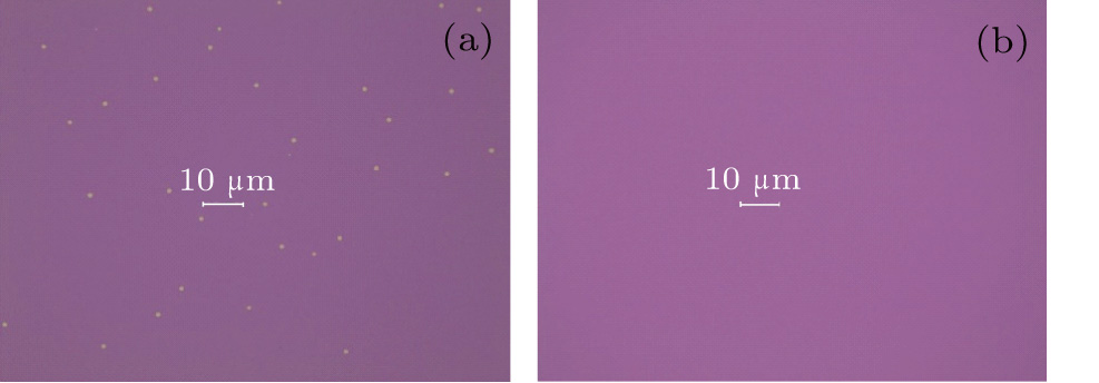
Figure 6 displays the dependence of the blistering phenomenon on SiO2 grown between the Al2O3 film and the silicon substrate at 450 °C. It can be clearly seen that when a SiO2 film grown by the NAOS method is introduced between Al2O3 and the silicon substrate, H escapes to the NAOS-SiO2 film after annealing at 450 °C. It did not overflow to the surface, which significantly suppresses the blistering phenomenon.
Fig. 6. Blistering phenomenon of the passivation stacks: (a) Al2O3/SiO2 at 450 °C, (b) SiO2/Al2O3/SiO2 at 450 °C.
As can be seen from Fig. 7, the minority carrier lifetime varies with the dose ratio of TMA to H2O in the ALD reaction source. As the ratio of TMA and H2O decreases, the amount of Al drops, which causes the amount of negative fixed charge in the Al2O3 to decrease and the amount of positive fixed charge in the stacks to increase. The increase in the number of positive charges optimizes the field effect passivation of the n-type substrate and enhances the minority carrier lifetime. Finally, the optimal value was obtained in the ratio of 1 : 4.
Fig. 7. Relationship between the minority carrier lifetime and the ratio of TMA and H2O.
Figure 8 indicates the dependence of C–V curves on the ratio of TMA and H2O. Compared with other dose ratios of TMA and H2O, when it is 1 : 4, the C–V curve shifts to the left, that is, the amount of positive fixed charge is the largest, which means that the field passivation plays an important role.
Fig. 8. Dependence of C–V curves on the ratio of TMA and H2O.
3.2. Annealing passivation effect
The relationship among the minority carrier lifetime and the first and second annealing temperatures can be seen from Fig. 9, where the first annealing is to activate the Al2O3 film, and the second annealing is to optimize the passivation of the SiO2/Al2O3/SiO2 stacks. When the first annealing temperature is controlled at 400 °C, the activation state of the Al2O3 film is the best. As the temperature becomes higher, the H contained in the Al2O3 film will overflow, which weakens the chemical passivation effect. However, when the temperature is lower than 400 °C, the Al2O3 film is not completely activated, and the passivation effect is also weakened. For the second annealing, the optimum annealing temperature is changed to 450 °C. This may be due to the presence of a certain amount of H after depositing the second SiO2 layer. Therefore, avoiding the passivation effect becoming bad will require a higher annealing temperature.
Fig. 9. Relationship between minority carrier lifetime and (a) first annealing temperature, (b) second annealing temperature.
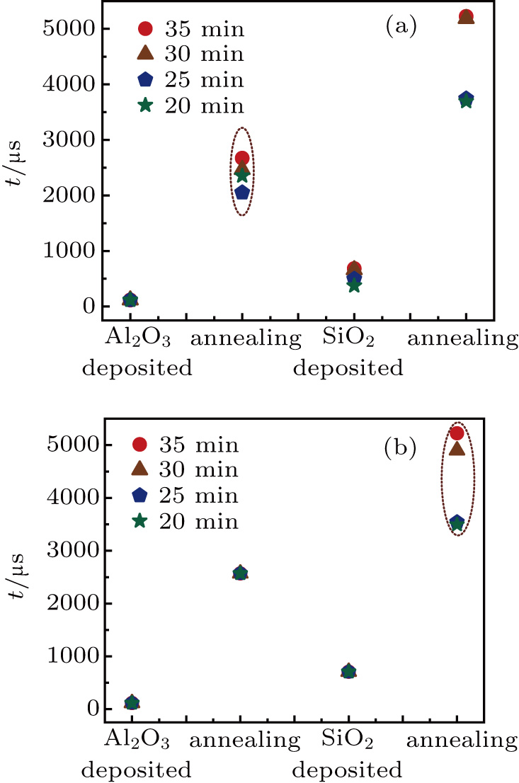
Figure 10 reveals the minority carrier lifetime as functions of first annealing and second annealing time. It can be seen from the figure that the lifetime of the minority carriers increases with the enhancement of annealing time. However, when the annealing time reaches 30 min, the optimization of the passivation layers nearly reaches the saturation value. Although there is a slight increase in minority carrier lifetime when the annealing temperature exceeds 30 min, the improvement is not small. Taking time and cost considerations into account, the annealing time of 30–35 min is enough.
Fig. 10. Minority carrier lifetime as functions of (a) first annealing time and (b) second annealing time.
Figures 11(a) and 11(b) depict the relationship between the minority carrier lifetime and the first and second annealing ambient. It can be seen from Fig. 11(a) that after depositing the Al2O3 film, the annealing ambient environment of forming gas (FGA) is preferable. This is because annealing at 10% H2 condition can offer a certain H compensation to the passivation stacks, which can saturate the dangling bond to optimize the passivation effect. The minority carrier lifetime in compressed air (CA) is obviously better than that of N2 in the first annealing, which is due to the presence of a certain amount of oxygen element in the CA. The deposited Al2O3 film belongs to the oxygen vacancies. Annealing in a certain amount of oxygen element can provide oxygen in these vacancies, which reduces the dangling bonds. Furthermore, figure 11(b) shows that the amount of fixed charge does not change at different annealing ambient environments, which means that the different minority carrier lifetimes in FGA, N2, and CA are mainly caused by chemical passivation. The reason for the best effect at the FGA annealing ambient environment of Fig. 11(c) is the same as Fig. 11(a). N2 and CA are both playing a role of insulation at the second annealing, so there is no big difference.
Fig. 11. (a) Minority carrier lifetime versus the first annealing ambient environment, (b) C–V curves for stacks of the first different annealing ambient environment, (c) minority carrier lifetime versus the second annealing ambient environment.
3.3. SiO2/Al2O3/SiO2 stacks applied to SDD
Figure 12 is an SEM image of the SiO2/Al2O3/SiO2 stacks applied to the SDD. The first SiO2 film grown by the NAOS method is too thin (about 1.2 nm) to show in this graph, but we tested it by ES.
Figure 13 is the test structure of the SDD. Table 1 shows the applied voltages of electrodes. The voltage between the collecting anode and the guard ring is 0 V. The voltage of back contact is −100 V. The voltage of the inner ring is −10 V. The voltage of the outermost ring varies from −200 V to 0 V. Figure 14 exhibits the SDD we made.
Figure 15 illustrates the relationship between leakage current of the SDD and the voltage of the outermost ring at different passivation modes. The experimental results were obtained at room temperature. The thickness of the SiO2 film grown by the thermal oxygen and PECVD is both 600 nm. From Fig. 15, we can find that the leakage current of the SDD increases with the improvement of the applied voltage.
Fig. 15. The relationship between the dark current of the SDD and the outermost ring voltage at different passivation modes.
However, compared with the SiO2 film grown by the thermal oxygen and PECVD, when SiO2/Al2O3/SiO2 stacks are applied to the SDD, the leakage current is significantly reduced.
Table 1.
Table 1.
Table 1.
Voltage of electrodes.
.
Electrode
Voltage/V
collecting anode
0
guard ring
0
outermost ring
−200 to 0
inner ring
−10
back contact
−100
Table 1.
Voltage of electrodes.
.
Figure 16 shows the x-ray source (Am241) without alpha particle detected by the SDD using the SiO2/Al2O3/SiO2 stacks. When the leakage current of the SDD is reduced, the resolution improves, which causes the SDD to detect x-ray source successfully.
Fig. 16. Am241 source detected by the SDD using SiO2/Al2O3/SiO2 stacks.
4. Conclusion and perspectives
In order to lower leakage current of SDDs, we have propose a new passivation structure of SiO2/Al2O3/SiO2 stacks. The passivation structure combines chemical and field passivation well. At an injection level of 5 × 1015 cm−3, the minority carrier lifetime reaches 5223 μs. When we apply the new passivation structure to the SDD, leakage current eventually reduces to the nA level, which is greatly contributed to the detection resolution of SDDs.
AceroM CBeldarrainODuchMZabalaMGonzálezM BCampabadalF2015Spanish Conference on Electron DevicesFebruary 11–13, 2015Madrid, Spain708744310.1109/CDE.2015.7087443