† Corresponding author. E-mail:
Project supported by the National Key Research and Development Program of China (Grant Nos. 2016YFB0400803 and 2016YFB0401801) and the National Natural Science Foundation of China (Grant Nos. 61674138, 61674139, 61604145, 61574135, and 61574134).
In order to investigate the inherent polarization intensity in InGaN/GaN multiple quantum well (MQW) structures, the electroluminescence (EL) spectra of three samples with different GaN barrier thicknesses of 21.3 nm, 11.4 nm, and 6.5 nm are experimentally studied. All of the EL spectra present a similar blue-shift under the low-level current injection, and then turns to a red-shift tendency when the current increases to a specific value, which is defined as the turning point. The value of this turning point differs from one another for the three InGaN/GaN MQW samples. Sample A, which has the GaN barrier thickness of 21.3 nm, shows the highest current injection level at the turning point as well as the largest value of blue-shift. It indicates that sample A has the maximum intensity of the polarization field. The red-shift of the EL spectra results from the vertical electron leakage in InGaN/GaN MQWs and the corresponding self-heating effect under the high-level current injection. As a result, it is an effective approach to evaluate the polarization field in the InGaN/GaN MQW structures by using the injection current level at the turning point and the blue-shift of the EL spectra profiles.
The InGaN-based light emitting devices, such as the light emitting diodes (LEDs) and the laser diodes (LDs), have been commercially produced and been adopted to various applications, such as the solid-state lighting, the full-color display, and the laser projection.[1] One of the special features of III-nitride materials is the inherent polarization field, which origins from the spontaneous polarization and the piezoelectric polarization.[2] In InGaN-based optoelectronic devices grown on c-plane sapphire or free-standing GaN substrates, the polarization field bends the energy band diagrams in InGaN/GaN multiple quantum wells (MQWs) and the quantum wells are changed from rectangular to triangular ones.[3] The integral intensity of the overlapped wave functions between electrons and holes is reduced and the radiative recombination efficiency in MQWs is subsequently suppressed. Meanwhile, the existence of the polarization field results in a non-uniform carrier distribution in the InGaN quantum wells as well as the corresponding vertical electron leakage current, even in the case of an AlGaN electron blocking layer (EBL) is introduced.[4,5] The polarization field is one of the reasons of the efficiency droop for InGaN-based LEDs.[6]
In order to suppress the negative effects of the polarization field in the InGaN-based devices, many results have been reported on how to manipulate the polarization field in InGaN-based LEDs and LDs, such as the application of polarization-matched MQW,[7,8] the design of InGaN quantum well thickness,[9–11] the epitaxial growth on semi-polar or non-polar substrates,[12–14] the introduction of mechanical force,[15] and the thickness thinning of the sapphire substrates.[16,17] We have theoretically calculated the effects of the polarization field on the device performance of InGaN-based light-emitting diodes, the laser diodes, and the solar cells.[18–21] However, it is challenging to evaluate the polarization field before a completed device fabrication procedure. In this article, we present an experimental investigation of the EL spectra characteristics. Three InGaN/GaN MQW samples with different polarization fields are studied. Based on an EL spectra analysis, the polarization field is evaluated after the epitaxial growth.
Three samples of InGaN/GaN multiple quantum well (MQW) structures are grown on the c-plane sapphire substrates by using a ThomasSwan 3 × 2″ metalorganic chemical vapor deposition (MOCVD) system. The trimethylgallium, the trimethylindium, and the ammonia are used as Ga, In, and N precursors, respectively. The structure of the three MQW samples is composed of a low-temperature GaN buffer layer grown at 530 °C, a 1-μm silicon-doped n-GaN layer grown at 1060 °C with a Si concentration of 3 × 1018 cm−3, an unintentionally-doped InGaN/GaN MQW active region, a magnesium-doped p-GaN layer with a Mg concentration of 3 × 1019 cm−3, and a heavily magnesium-doped p++-GaN contact layer with a Mg concentration of 3 × 1020 cm−3. In the three-period InGaN/GaN MQW active region, the thickness of InGaN quantum wells is fixed to be 2.4 nm, while the thickness of GaN barrier is designed to be 21.3 nm, 11.4 nm, and 6.5 nm to intentionally change the polarization field.
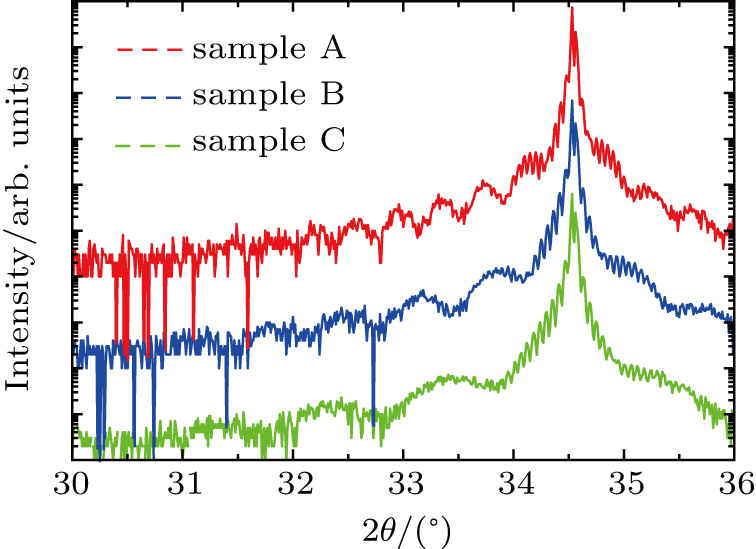
After the epitaxial growth in MOCVD system, the structures of the three MQW samples are firstly checked by using x-ray diffraction (XRD), as shown in Fig.
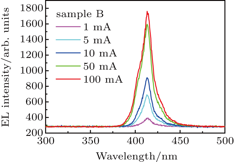
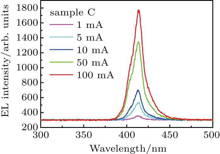
Then the electroluminescence (EL) spectra measurement is performed on a probe station with two needle contacts under different levels of the current injection. The injection current of 1 mA, 5 mA, 10 mA, 50 mA, and 100 mA is provided by an ITech IT6123 DC Source Meter as shown in Figs.
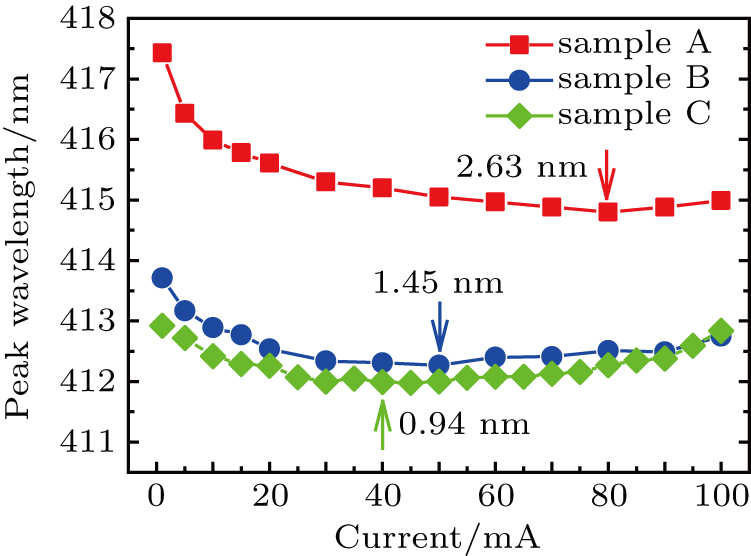
The EL spectra data of samples A, B, and C are collected with the injection current increases from 1 mA to 100 mA. Each spectra diagram is fitted by the Gaussian curve and the value of the peak wavelength is recorded for each fitting curve. The data of peak wavelength are shown in Fig.
However, detailed difference occurs for the spectra shift of samples A, B, and C. In the first place, the peak wavelength is different under the same current injection level, even though the samples have the same value of the well thickness and the indium composition in InGaN quantum wells. Under the same current injection level, sample A with the largest value of the GaN barrier thickness has the longest peak wavelength. Sample C with the smallest value of the GaN barrier thickness has the shortest peak wavelength. Secondly, the spectra have different values of the blue-shift. The maximal blue-shift value, which equals the difference between the longest and the shortest peak wavelengths in the spectra profile, is calculated to be 2.63 nm, 1.45 nm, and 0.94 nm for samples A, B, and C, respectively, as shown in Fig.
The phenomena of the EL spectra shift are attributed to the effect of the inherent polarization field in InGaN/GaN MQWs. The polarization field in III–nitride materials is composed of two parts. The spontaneous polarization results from the lack of the inversion symmetry alone the c axis of the wurtzite crystal structure. The piezoelectric polarization is a result of the stress which comes from the lattice mismatch and the thermal mismatch. The energy band diagram of InGaN/GaN MQWs is sloped by the polarization field and the triangular quantum wells are thus formed.
When the thickness of the GaN barrier increases from 6.5 nm to 21.3 nm, the stress in the InGaN quantum wells rises and the piezoelectric polarization is enhanced. For the sample with thicker GaN barrier, the gradient of the energy band diagram in InGaN quantum wells is larger than that of other two samples. The quantum-confined Stark effect (QCSE) is correspondingly enhanced, leading to a longer peak wavelength under the low-level current injection,[22] as shown in Fig.
When the current injection level rises, more carriers are injected into the InGaN quantum wells, the impact of the polarization field tends to be weakened by the Coulomb screening effect and the band-filling effect,[23,24] exporting a rise of the EL spectra blue-shift of the peak wavelength. For samples A–C, when the thickness of the GaN barrier increases from 6.5 nm to 21.3 nm, the polarization field in the InGaN quantum wells is enhanced.[25] The maximum value of the spectra blue-shift rises from 0.94 nm for sample C to 1.45 nm and 2.63 nm for samples B and A, respectively, as shown in Fig.
The polarization field and the energy band bending also have an effect on the vertical electron leakage in the InGaN/GaN MQW structures. For the carriers injected into the InGaN/GaN MQW, parts of them are captured inside the InGaN quantum wells. Another part escapes from the quantum wells and migrates to the p-doped region, and thus generates the vertical electron leakage current.[26–29] These leaked electrons contribute to the non-radiative recombination and the heat generation. When the current injection level continuously rises, the vertical electron leakage current and the heat generation increases. The EL spectra shows a tendency of the red-shift with a higher temperature, known as the self-heating effect.[30–32]
The variation of the turning point in EL spectra is determined by the vertical electron leakage. With the existence of the polarization field, the energy band diagram is tilted and the triangular quantum wells are formed. When the barrier thickness increases, the polarization field is enhanced. For a quantum well with a higher effective depth, a larger amount of the electrons are needed to full-fill the low energy levels. For the sample with a thicker barrier, the vertical electron leakage will be reduced, and the heat generation is weakened under the same current injection level. The improvement of the thermal stability puts off the beginning of the red-shift in the EL spectra and a larger value of the turning point is thus obtained. Since the red-shift value is sensitive to the heat management, a temperature-controlled probe stage will be helpful to get a more precise result.
Based on the spectra analysis mentioned above, the comparison of the polarization field in the InGaN MQW samples can be presented by the maximum value of the blue-shift in the EL spectra. A larger value of the spectra blue-shift and the turning point indicates a higher intensity of the polarization field in InGaN/GaN MQWs. The experimental results and the subsequent spectra analysis will benefits the design of the InGaN/GaN MQW devices. It is usually challenging to characterize the polarization field before the device fabrication is completed. Based on our study, the features of the polarization field can be extracted from the EL spectra and the analysis of the corresponding effects can be evaluated.
An EL spectra analysis approach is proposed to evaluate the effects of the polarization field in the InGaN/GaN MQW structures. Three samples of InGaN/GaN MQWs with difference barrier thicknesses of 21.3 nm, 11.4 nm, and 6.5 nm are prepared. Under the same current injection level, the peak wavelength of samples A–C differs from one another. Sample A with the highest value of the barrier thickness has the largest value of the peak wavelength. When the current injection level increases, the peak wavelength of the EL spectra firstly shows a blue-shift and then turns to be red-shifted. The maximum value of the blue-shift is measured to be 2.63 nm, 1.45 nm, and 0.94 nm for samples A, B, and C, respectively. It is considered to be closely related to the polarization field inside the InGaN quantum wells. The value of the turning point, which is 80 mA, 50 mA, and 40 mA for samples A–C, indicates the difference of the vertical electron leakage current from the InGaN quantum wells to the p-type layers. Based on our experimental results, the polarization field can be simply evaluated by the analysis of the EL spectra data.
| [1] | |
| [2] | |
| [3] | |
| [4] | |
| [5] | |
| [6] | |
| [7] | |
| [8] | |
| [9] | |
| [10] | |
| [11] | |
| [12] | |
| [13] | |
| [14] | |
| [15] | |
| [16] | |
| [17] | |
| [18] | |
| [19] | |
| [20] | |
| [21] | |
| [22] | |
| [23] | |
| [24] | |
| [25] | |
| [26] | |
| [27] | |
| [28] | |
| [29] | |
| [30] | |
| [31] | |
| [32] |


