† Corresponding author. E-mail:
Project supported by the National Natural Science Foundation of China (Grant Nos. 61874058, 51861145301, and 61376023), the National Key Basic Research Program of China (Grant No. 2015CB932203), China Postdoctoral Science Foundation (Grant No. 2018M642283), the Synergetic Innovation Center for Organic Electronics and Information Displays, China, and the Priority Academic Program Development Fund of Jiangsu Higher Education Institutions (PAPD) in China.
Polarized red, green, and blue light emitting diodes (LEDs) are successfully fabricated using polyfluorene and its derivatives, namely, poly (9,9-dioctylfluorene) (PFO), poly (9,9-dioctylfluorene-co-benzothiadiazole) (F8BT), and poly (triphenylamine-co-4,7-di(thiophen-2-yl)benzo[c][1,2,5]thiadiazole-co-benzo[c]thiadiazole-co-9,9-dioctyl-9H-fluorene) (Red F). Rubbed hole transport layer poly(3,4-ethylenedioxythiophene): poly(styrene sulfonate) (PEDOT:PSS) is employed in the devices as the alignment layer to achieve fully monodomain alignment in all polymer layers. Red F is blended with F8BT to realize the polarized electroluminescence of red light (dichroic ratio ∼3.3), despite having no liquid crystallinity itself. Comparing PFO/F8BT blend to F8BT, higher efficiency of polarized emission is found due to the energy transfer. All the polarized LEDs exhibit pronounced dichroism and efficient polarized emission compared to the non-alignment regular devices.
Organic semiconductors attract considerable attention due to their unique merits in chemical structure tunability, solution processability, and mechanical flexibility.[1] The organic optoelectronic devices are widely developed and intensely studied in the fields of light emitting diodes,[2,3] solar cells,[4,5] field effect transistors,[6,7] and plastic lasers.[8–10] Among the applications, organic light emitting diodes (OLEDs) were firstly exploited and possess the most promising future. Due to the strong demand from the consumer market and continuous efforts devoted by the manufacturers, OLEDs technology has been regarded as the solution for the next generation display of smartphones, laptops, and televisions. In recent years, polarized emission from liquid crystal materials has drawn growing interests from both academic and industrial circles because of the potential in optoelectronic applications, including backlight sources for conventional liquid crystal displays (LCDs),[11] three-dimensional imaging,[12] and so on. Unlike the traditional method of combining a polarizer with an unpolarized light source for achieving light polarization, OLEDs with aligned active layer can directly produce polarized emission,[13–15] which avoids waste of the ∼50% production light. The emission dichroic ratio, 
In this work, polyfluorene, poly (9,9-dioctylfluorene) (PFO) and its derivatives, poly (9,9-dioctylfluorene-co-benzothiadiazole) (F8BT) and poly (triphenylamine-co-4,7-di(thiophen-2-yl)benzo[c][1,2,5] thiadiazole-co-benzo[c] thiadiazole-co-9,9-dioctyl-9H-fluorene) (Red F) are used as the active materials for polarized LEDs. The non-liquid-crystallinity behavior polymer, Red F, can also achieve a certain degree of anisotropy through physical mixing with F8BT and benefit from the energy transferring in the meantime. The PFO/F8BT (5 wt.% F8BT) shows similar dichroic ratio in absorption/emission and results performance-enhanced LEDs, comparing to F8BT itself. The red, green, blue (RGB) light emitting diodes using the same rubbed alignment PEDOT:PSS layer are realized with identical device configuration. Reasonable dichroic ratio value is achieved in all polarized LEDs with simple device fabrication.
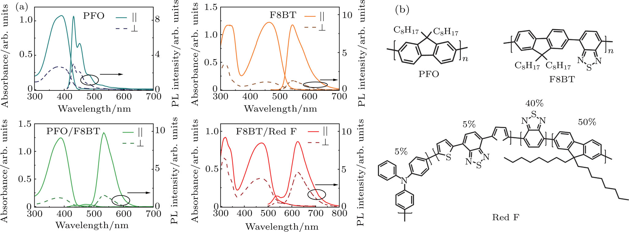
The polymers used in this work are commercially available compounds, polyfluorene and its derivatives, namely, PFO, F8BT, and Red F (chemical structures shown in Fig. 


Some early reports[34,35] claimed that the possible damage to the PEDOT:PSS layer during the rubbing procedure will affect the performance of the resulting polarized LEDs. Nevertheless, the atomic force microscopy (AFM) image of the rubbed PEDOT:PSS layer (on ITO glass) shows a root-mean-square (RMS) roughness of 0.78 nm with no evidential thread of scratching (see Fig. S2 in supporting information). The morphology of the aligned polymer films (thickness ∼70 nm) deposited on top of the PEDOT:PSS layer is also considerable uniform for all polymers (RMS roughness ∼1.21 nm for PFO, 0.86 nm for F8BT, ∼1.22 nm for PFO/F8BT, and 1.61 nm for F8BT/Red F) and shows no phase separation in the blends, which will facilitate the device fabrication.
To understand if the rubbed PEDOT:PSS layer in our work (protocol in experimental section) can fully align the polymers on top, the dependence of the absorption dichroic ratio on film thickness is investigated (see Fig. S3 in supporting information). The maximum thicknesses of the polymer films that can be fully aligned are 92 nm for PFO, 112 nm for F8BT, 73 nm for PFO/F8BT, and 166 nm for F8BT/Red F blend. These values all exceed the thickness of active layers used in the LEDs fabrication hereinafter.
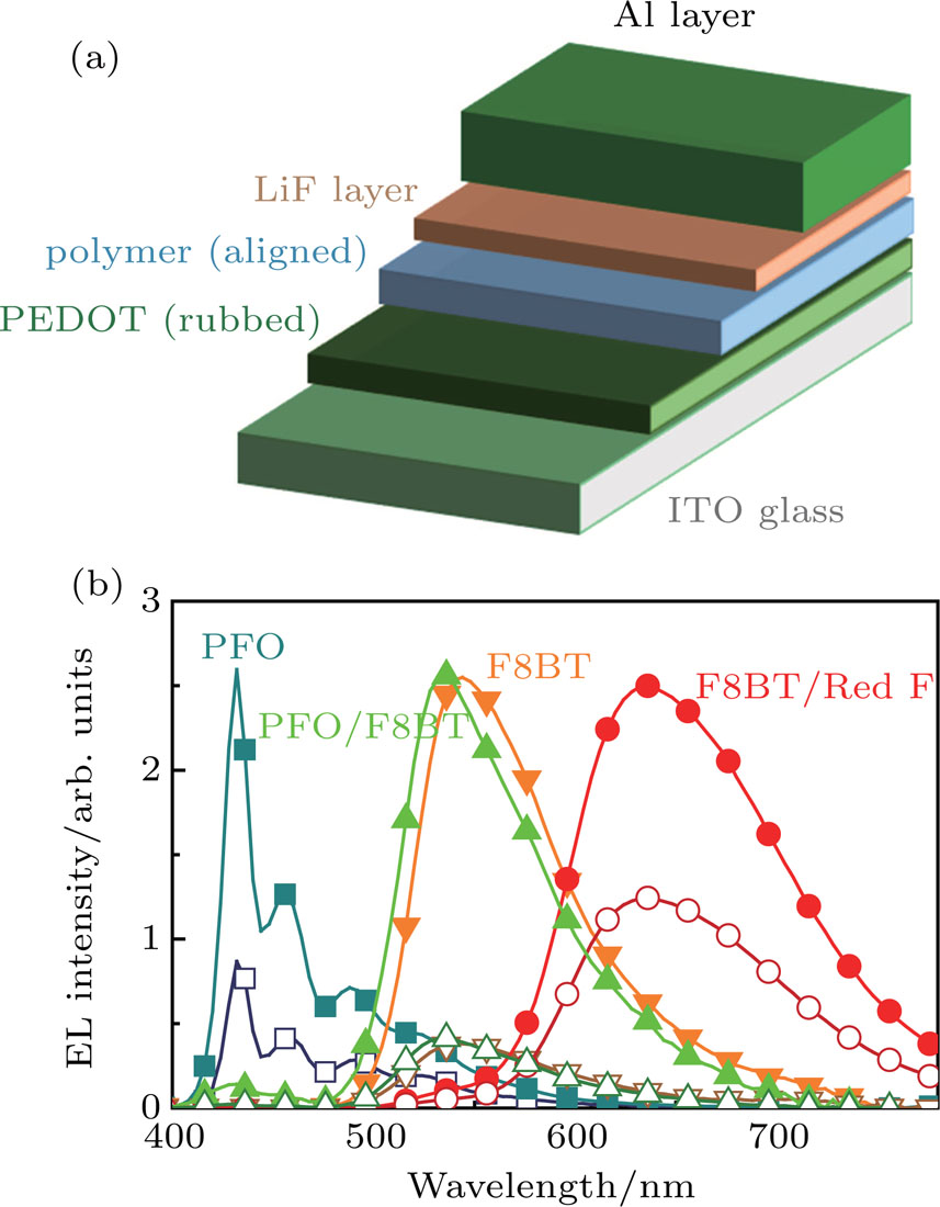
The LED configuration involved in this work is presented in Fig. 


| Table 1.
Key parameters of the polarized devices. |
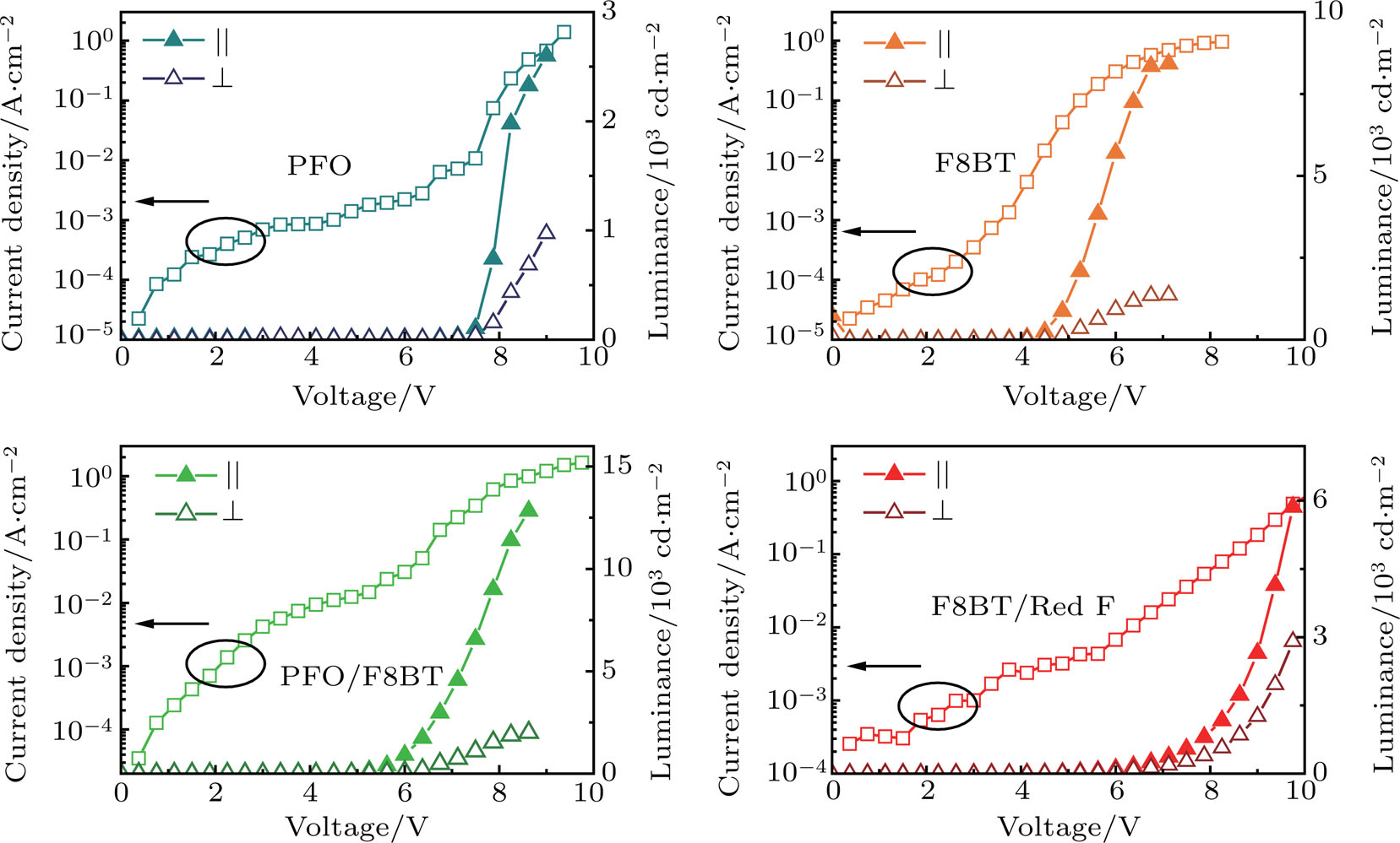
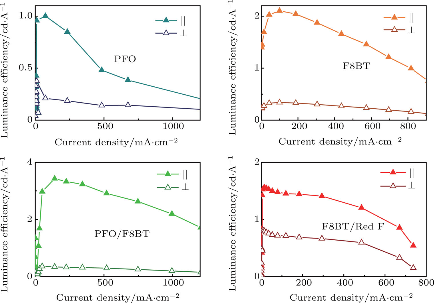
Correspondingly, the polarized maximum luminance current efficiencies 


Reasonable dichroic ratios are achieved in all the samples, confirming that the rubbed PEDOT:PSS hole transport layer enables built-in polarized RGB light emission from simply-constructed LEDs with polyfluorene and its derivatives. In contrast, for regular devices, polarized emission can be achieved only by coupling the output light with an additional polarizer in the price of losing more than half of the brightness and luminance efficiency due to extra scattering and reflection loss (see Figs. S4 and S5 in supporting information). Obviously, using the built-in polarized LEDs demonstrated above is a more efficient and inexpensive solution for the next generation OLED displays or illumination under certain circumstances.
PEDOT:PSS (BAYTRON 


The ITO glass or polished synthetic quartz substrates were ultrasonically cleaned by detergent, deionized water, acetone, and ethanol. After drying, they were treated by plasma (PLASMA-PREENII-862) at the power of 70 W for 4 min to remove residual organic impurities on the surface and to improve the hydrophilic properties of the top surface. A PEDOT:PSS alignment layer (30 nm thick) was deposited following by annealing at 120 °C for 20 min. After cooled down to room temperature, alignment treatment was carried out by surface rubbing with a home-made machine which contains an electromotor driven drum covering with a velvet cloth.
The conjugated polymer films were then spin-coated onto rubbed PEDOT:PSS from the pre-stirred solution. The adjustment of the film thickness was achieved by changing the spin-coating speed. To achieve chain orientation, the PFO film was annealed at 200 °C for 2 min in nitrogen atmosphere, then cooled down to 170 °C at a speed of 1 °C/min and quenched to room temperature. F8BT, PFO/F8BT blend, and F8BT/Red F blend films were annealed at 265 °C for 2 min in nitrogen atmosphere, then cooled down to 235 °C at 1 °C/min and quenched to room temperature. The hot plate used for annealing treatment was a LINKAM LTS420E-PB4 probe hot stage.
Film morphology tests were carried out at room temperature using a Bruker Dimension Icon AFM equipped with Scanasyst-Air peak force tapping mode atomic force microscope (AFM) tips from Bruker.
The absorption and photoluminescence spectra of the samples were measured at room temperature using Lambda 35 UV/VIS spectrophotometer and PerkinElmer LS55 fluorescence spectrophotometer. In absorption measurements, a polarizer (Thorlabs) was placed in front of the incident light slit for generating polarized light parallel or perpendicular to the direction of the oriented polymer chain. In PL measurements, the same polarizer was placed in front of the light collecting slit to couple the polarized emission from the sample.
Rubbed PEDOT:PSS layer was fabricated on the ITO glass as described above followed by active layer deposition. The thickness of the emission layer was controlled to be 70 nm by changing the speed of spin coating (PFO@4000 rpm, F8BT@4500 rpm, PFO/F8BT@4000 rpm, F8BT/Red F@5500 rpm). Thermal annealing was then employed following the protocol described above to orient the polymer chain. Samples with well-aligned emissive layers were then transferred into a thermal evaporator. 1 nm LiF and 120 nm Al were evaporated onto the polymer in sequence under high vacuum (10−5 bar). The device structure is shown in Fig.
The red, green, blue polarized LEDs are fabricated successfully with the same device configuration using a rubbed PEDOT:PSS layer as both the alignment and hole transport layer. For the non-liquid-crystal polymer compound Red F, through blending with F8BT, the resulting device shows clear dichroism. All polymer layers used in the LEDs can be fully aligned through the identical simple treatment. The performance of the resulting LEDs is not affected by the rubbing or thermal treatment, comparing to the control devices without aligned active layers. The EL dichroic ratios of the LEDs constructed in this work are 3.0, 6.7, 6.2, and 2.0 for the PFO, F8BT, PFO/F8BT, and F8BT/Red F blend-based devices, respectively. Efficient energy transfer in the PFO/F8BT blend results better LED performance with higher maximum luminance and LE, comparing to those of F8BT itself. The RGB built-in polarized LEDs demonstrated in this work can possibly be further integrated together on the same piece of substrate acting as the polarized-emitting pixel in future display plane or illumination source.
| [1] | |
| [2] | |
| [3] | |
| [4] | |
| [5] | |
| [6] | |
| [7] | |
| [8] | |
| [9] | |
| [10] | |
| [11] | |
| [12] | |
| [13] | |
| [14] | |
| [15] | |
| [16] | |
| [17] | |
| [18] | |
| [19] | |
| [20] | |
| [21] | |
| [22] | |
| [23] | |
| [24] | |
| [25] | |
| [26] | |
| [27] | |
| [28] | |
| [29] | |
| [30] | |
| [31] | |
| [32] | |
| [33] | |
| [34] | |
| [35] |


