


Dark count rate and band to band tunneling optimization for single photon avalanche diode topologies
Cite this Article
Haddadifam Taha, Azim Karami Mohammad. Dark count rate and band to band tunneling optimization for single photon avalanche diode topologies. Chinese Physics B, 2019, 28(6): 068502 
Permissions
Dark count rate and band to band tunneling optimization for single photon avalanche diode topologies
† Corresponding author. E-mail:
Abstract
This paper proposes two optimal designs of single photon avalanche diodes (SPADs) minimizing dark count rate (DCR). The first structure is introduced as p+/pwell/nwell, in which a specific shallow pwell layer is added between p+ and nwell layers to decrease the electric field below a certain threshold. The simulation results show on average 19.7% and 8.5% reduction of p+/nwell structure’s DCR comparing with similar previous structures in different operational excess bias and temperatures respectively. Moreover, a new structure is introduced as 

1. Introduction
Digital silicon photomultipliers (dSiPMs) are new elements for detecting low-level light with unique features such as high photon-detection efficiency, single photon timing resolution, low operating voltage, magnetic field insensitivity, high uniformity, compact form factor, low gain drift, high degree of scalability, and high ruggedness.[1,2] Moreover, dSiPMs have numerous applications in different fields of science such as positron emission tomography (PET) and single photon emission computed tomography (SPECT).[2,3]
The light sensitive area in dSiPMs is divided into an array of single photon avalanche diodes (SPADs). An SPAD pixel consists of multiple components like p–n junction, guard rings and quenching, sensing and recharging circuits.[4] Each SPAD functions like a digital sensor which detects single photon absorption. In fact, an SPAD itself is a p–n junction biased above breakdown voltage operating in the Geiger mode.[2] In addition, every SPAD has a depletion region and a multiplication region inside. A multiplication region is an area inside depletion region where avalanche multiplication occurs. Once a photon enters silicon, it can be absorbed in the depletion region and produces an electron-hole pair. Then, the electric field in this region separates electron and hole and accelerates them in opposite directions.[5] One of the positive concepts of the dSiPM’s operation is that detecting the avalanche in SPADs is based on the sensing voltage changes. Thus, this makes the sensor response faster and less sensitive to the gains of the individual SPADs.[2]
Despite these distinct features, dSiPMs suffer from high dark count rate (DCR). In the absence of light, because of the thermal excitation, minority carriers are generated to induce avalanche events recognized as dark counts.[5] DCR in these detectors almost consists of band to band tunneling (BTBT), Shockley Read Hall (SRH), and trap assistant tunneling (TAT). These detectors have high DCR in comparison with other detectors like photomultiplier tubes (PMTs) in higher excess biases and temperatures.[6] Due to the dSiPM’s total DCR equation which is the summation of pixel DCRs, these detectors have high amount of DCR especially in large array SPADs. Some characteristics of dSiPMs like signal-to-noise ratio (SNR) and dynamic range (DR) are inversely dependent on DCR value. Hence, more DCR also causes less DR and SNR.[7] Different methods are proposed to reduce DCR such as pixel masking and temperature reduction.[8,9] However, in the present work, new SPAD structures are proposed for dSiPMs to decrease DCR.
The novelty of this work is adding one extra layer to previous structures to reduce the electric field in order to reduce DCR. Hence, the pwell layer is added to the p+/nwell structure and nwell layer is added to the n+/pwell structure. By adding these layers, the electric field is under control and DCR will be reduced. Some dSiPMs which include p+/nwell structure for SPADs have high BTBT and DCR. Therefore, using these modified structures as SPADs will decrease DCR.
The rest of this paper is organized as follows The theoretical methods which are needed to describe SPADs operations are introduced in Section 2. In Section 3, new structures are proposed with simulation results. Finally, the analysis is given in analysis and discussion section to demonstrate the efficiency of the proposed structures in higher excess biases and temperatures.
2. DCR calculation
DCR can be calculated using[5]


3. Design and description
3.1. p

/pwell/nwell structure
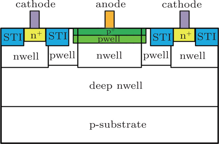
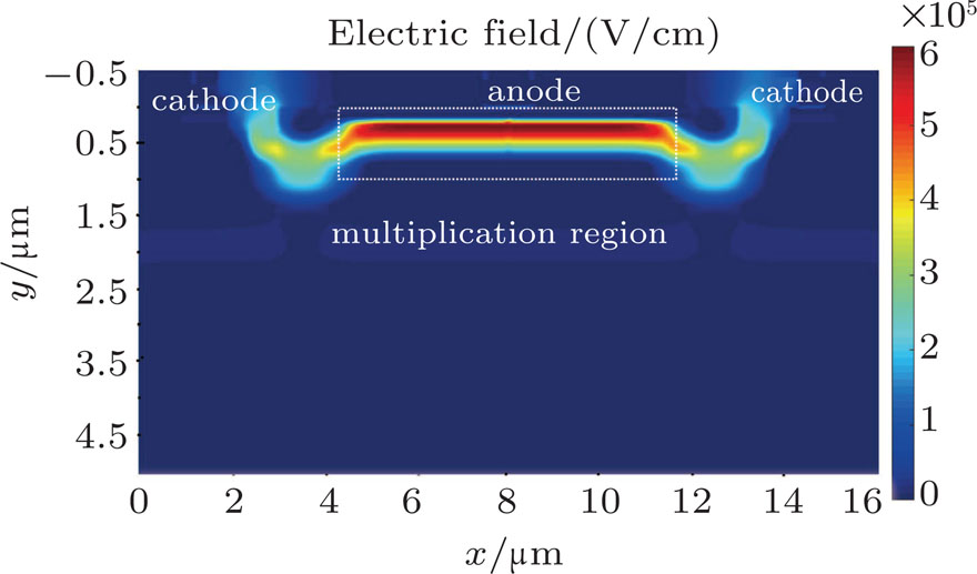
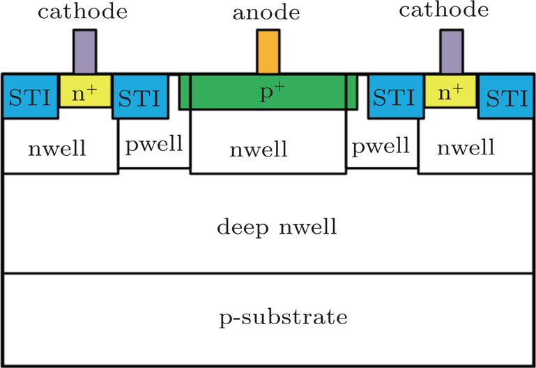
In the proposed structure, which is based on [5] and has been modified in this paper, the p+/pwell/nwell junction is surrounded by pwell and shallow trench isolation (STI) guard rings, which prevents premature breakdown at p–n junction edges. The deep nwell layer isolates the SPAD from other devices.[5] A wide depletion junction which comprises pwell/nwell is used to lower BTBT and DCR.[14,15]
A thin p+ layer is implanted on the device surface to form Ohmic contact and to prevent enhancing DCR of the device.[16] On the other hand, this layer contributes to high DCR since it increases electric field at depletion region edges. In order to have p+ presence advantages and lower electric field, a pwell layer is implanted under p+ layer. It should be mentioned that the depth of new pwell layer is less than pwell guard rings and its doping is considered higher than pwell guard rings. This could be performed with halo implants. Halo doping is used for increasing the doping in specific areas.[17,18] By using this approach, the doping of this layer is enhanced to meet specific value of electric field in order to have avalanche event. Implanting new pwell layer in this structure leads device to have lower DCR due to the lower electric field. However, using p+/pwell/nwell structure instead of p+/nwell structure affects SRH minimally due to TAT model. In addition, by using a thinner layer of p+, timing response will be improved.[19] Figure
 | Fig. 1. p+/pwell/nwell structure. |
 | Fig. 2. Two-dimensional (2D) electric field profile of p+/pwell/nwell structure. |
The nwell layer’s doping also affects the electric field and DCR. Higher concentration of nwell doping can be translated as higher DCR,[20] though nwell doping decrement has a limitation. Indeed, this region’s doping could be lowered until a certain threshold. The limitation exists because the electric field attenuates and the avalanche event does not occur when nwell doping decreases below a certain threshold. Eventually, it should be noted that the PDE of this device is about 12.8% and less than p+/nwell structure’s PDE (17.5%) in 300 nm wavelength and 3.5 V excess bias due to lower avalanche probabilities.
3.2. n+/nwell/pwell structure
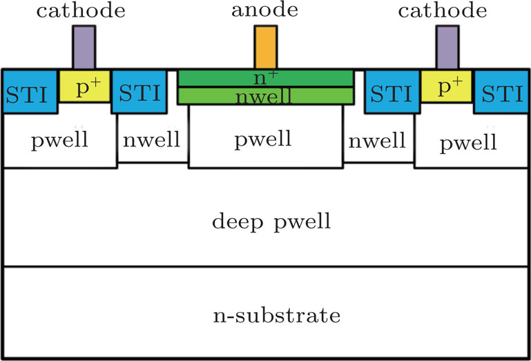
In this structure, which is based on [21] and has been modified, the n+/nwell/pwell junction is surrounded by nwell and STI guard rings, which prevent premature breakdown to occur at p-n junction edges. The deep pwell layer isolates the SPAD from other devices. A wide depletion junction which comprises nwell/pwell is used to have a lower BTBT and DCR.[14]
A thin n+ layer is implanted on the device surface to create ohmic contact with the metal and to impede DCR of the device from enhancement.[16] On the other hand, this layer contributes to high DCR since it increases electric field at the edge of the depletion region. To have the advantages of n+ presence and lower electric field, a nwell layer is implanted under the n+ layer. Again, same as previously proposed structure, it should be mentioned that the depth of this layer is less than pwell guard rings and its doping is considered higher than pwell guard rings with the usage of halo implant.[18] Hence, the doping of additional nwell layer is enhanced to meet specific value of electric field in order to have avalanche event.
In conclusion, the device has lower DCR due to lower electric field. However, using n+/nwell/pwell structure instead of p+/nwell structure affects SRH minimally due to TAT model. In addition, by using a thinner layer of n+, timing response will be improved.[19] Another concept that occurs in the proposed structure is that the holes are minority carriers. Thereby, the avalanche probabilities are less than the situation where electrons initiate avalanche. Therefore, this device has low PDE. Namely, nwell and pwell layers play a key role in decreasing DCR by electric field reduction.
The pwell layer’s doping also affects the electric field and DCR. Higher pwell doping can be translated as higher DCR.[20] Decreasing pwell doping has a limitation. Indeed, this region’s doping could be lowered until a certain threshold. The limitation exists because the electric field attenuates and the avalanche event does not occur when pwell doping is lowered below the certain threshold. Figure
 | Fig. 3. n+/nwell/pwell structure. |
4. Simulation results
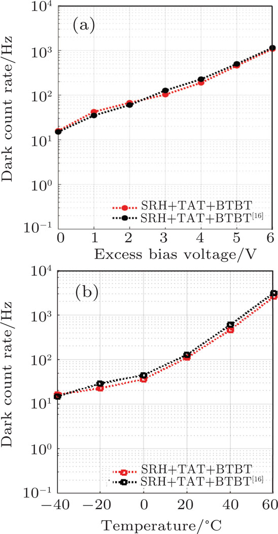
To compare the results of this paper with the previous data, the p+/nwell structure is considered as a reference.[5,16] The p+/nwell structure’s DCR, BTBT, and SRH/TAT are verified to have certain criteria for comparing results of the simulations. Figure
 | Fig. 4. p+/nwell structure. |
 | Fig. 5. Verified results. DCR values in: (a) excess bias voltage and (b) temperature variations. |
Table
| Table 1.
The important characteristics of both n+/nwell/pwell and p+/pwell/nwell structures. . |
Table
| Table 2.
Simulation parameters. . |
4.1. p+/pwell/nwell structure analysis
In this section, the p+/pwell/nwell structure is simulated in excess bias variation from 0 V to 6 V. In addition, simulations are performed in temperature variation from −40°C to 60 °C.
4.1.1. Excess bias variation
In Fig.
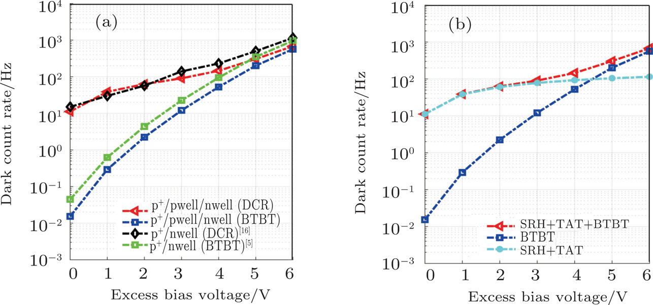 | Fig. 6. (a) BTBT, SRH/TAT, and DCR of p+/pwell/nwell structure at room temperature. (b) Comparison between p+/pwell/nwell and p+/nwell[5,16] structures. |
Figure
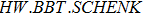
4.1.2. Temperature variation
Figure
4.2. n+/nwell/pwell structure analysis
In this section, the n+/nwell/pwell structure is simulated in excess bias variation from 0 V to 6 V. In addition the structure is simulated in temperature variation from −40°C to 60 °C.
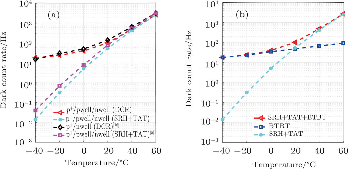
4.2.1. Excess bias variation
Figure
4.2.2. Temperature variation
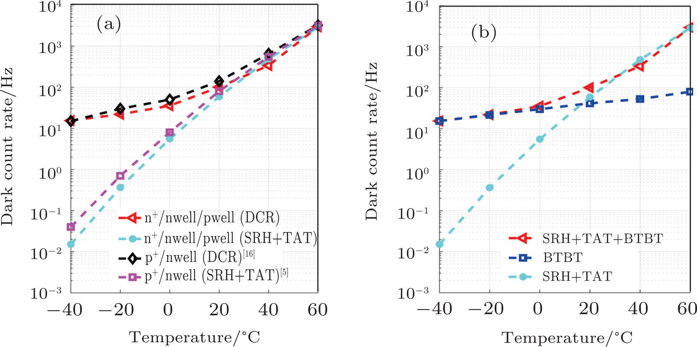
The comparisons of DCR and SRH between n+/nwell/pwell and p+/nwell[5,16] structures in temperature variation are shown in Fig.
5. Results and discussion
5.1. p+/pwell/nwell structure
The results and figures indicate that DCR and BTBT are less than those in [5] and [16] in excess bias variation and more than those of n+/nwell/pwell structure. In addition, DCR and SRH of this structure are less than those in [5] and [16] and n+/nwell/pwell structure in temperature variation. However, to quantitatively evaluate the improvement (DCR reduction), the difference between the DCR of p+/nwell structure and the DCR of p+/pwell/nwell structure is averaged in different biases or different temperatures, and the mean difference is calculated for DCR, BTBT, and SRH quantities.
In excess bias variation (between 0 V to 6 V), mean difference value between BTBTs is 49%. In other words, this proposed structure reduces BTBT of p+/nwell[5,16] by 49%. In addition, this structure diminishes DCR of p+/nwell[5,16] leastwise 19.7%. In temperature variation (between −40 °C to 60 °C), the mean difference value between SRHs is 15.2% and this structure diminishes DCR of p+/nwell[5,16] by 8.5%.
5.2. n+/nwell/pwell structure
In this section, similar to the previous section, mean difference values are evaluated. In excess bias variation (between 0 V to 6 V), the mean difference value between BTBTs is 61.9%. Moreover, the n+/nwell/pwell structure diminishes DCR of p+/nwell[5,16] by 29.2%. Eventually, in temperature variation (between −40° to 60 °C), mean difference value between SRHs is 12.1% and this structure lessens DCR of p+/nwell[5,16] by 5.5%.
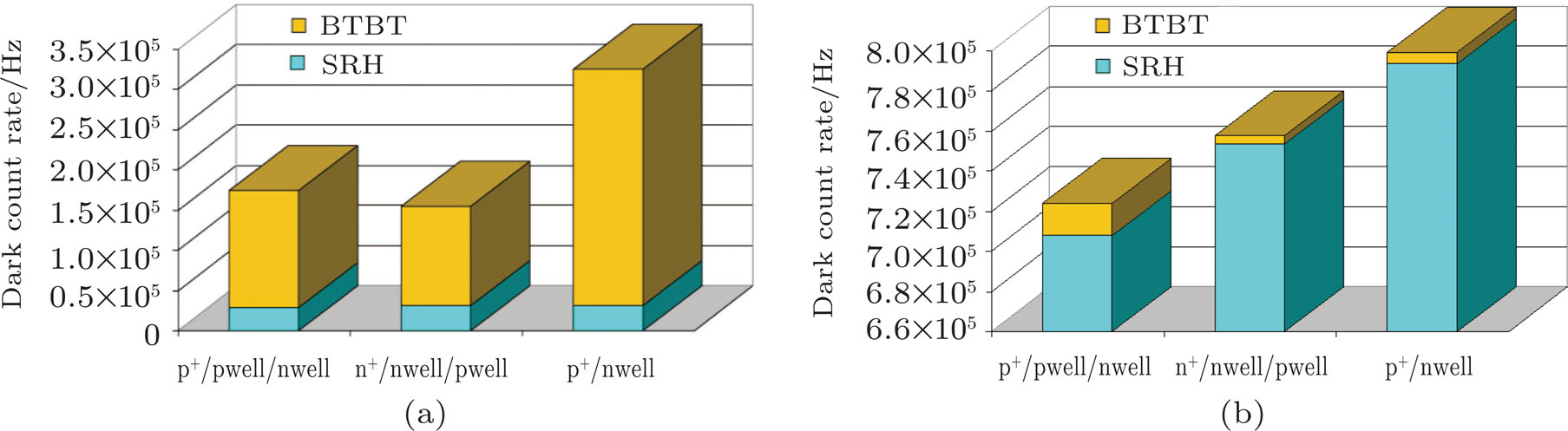
The DCR improvements become more tangible for using in a dSiPM including an array of several SPADs. Thus, using p+/pwell/nwell and n+/nwell/pwell structures for SPAD in dSiPM could diminish the total DCR of dSiPM. Figure
 | Fig. 10. DCR comparison between three structures of a high voltage dSiPM. (a) DCR at 6-V excess bias (room temperature). (b) DCR at 60 °C (3.5-V excess bias). |
Due to obtained results and Fig.
6. Conclusions
In this paper, two optimal designs of SPAD for dSiPM with the same pixel pitch of 
Reference
| [1] | |
| [2] | |
| [3] | |
| [4] | |
| [5] | |
| [6] | |
| [7] | |
| [8] | |
| [9] | |
| [10] | |
| [11] | |
| [12] | |
| [13] | |
| [14] | |
| [15] | |
| [16] | |
| [17] | |
| [18] | |
| [19] | |
| [20] | |
| [21] | |
| [22] | |
| [23] |