Gradient refractive structured NiCr thin film absorber for pyroelectric infrared detectors
School of Optoelectronic Information, University of Electronic Science and Technology of China (UESTC), Chengdu 610054, China
† Corresponding author. E-mail:
yuhe@uestc.edu.cn
Project supported by the National Natural Science Foundation of China (Grant Nos. 61875031 and 61421002).
1. IntroductionPyroelectric infrared detectors are commonly used to monitor infrared radiation in the wavelength range of
 and in military spacecraft in the wavelength range of
 .[1–3] To improve the sensitivity of pyroelectric infrared (IR) detectors, infrared absorbing layers have to meet the following demands:[4,5] (i) high and spectrally homogeneous radiation absorption, (ii) very low thermal mass, (iii) high heat conductivity, (iv) good long-term stability and reproducibility of the properties, and (v) their fabrication must be compatible with the detector manufacturing technology. Popular solutions that meet some of these requirements include thin metal films, resonant cavity structures, plasmonic metamaterials, porous surfaces, and vertically aligned arrays of carbon nanotubes (CNT). However, ultra-thin metal films are limited in terms of absolute absorbance and are not temperature stable.[6] Porous films and metal-blacks require well controlled etch chemistry and can be easily destroyed by physical contact.[7] Quarter wavelength cavity resonances are good solutions for selective detection with spectral bandwidths on the order of 10% or lower in the visible-IR range, but are not suitable for mid/long wave infrared and very long wavelength applications.[8] The principle of CNTs arrays is based on trapping light in the sparse and tall CNT arrays.[9,10] The height of the arrays (tens to hundreds of microns) allows for multiple internal reflections and the eventual absorption of all incident radiation over a large spectral range. Unfortunately, their large mass and thermal loading on the detector are drawbacks. In this work, we present a nano-structured NiCr alloy material with graded-refractive-index coating which has a high extinction coefficient k at infrared wavelength range. The absorber features high absorption efficiency (
 ) peaks in the wavelength of
 ,
,
 , and
, and
 . Its adhesion properties are also excellent, resulting from a denser layer deposited on the substrate. Other major benefits include the one-step deposition and the functional integration of the detectorʼs front electrode and the absorption layer, which are enabled by the sputtering deposition technique. The performance of the NiCr absorption layer is superior to that of single metal films in combination with good mechanically stability, making this an attractive material for use in IR detectors.
2. Experimental results2.1. Fabrication of nano-structured NiCr absorptionThe typical pyroelectric detector is structured with LiTaO3 material in a central layer between two metal electrodes. The pyroelectric detectors were fabricated from a polarized LiTaO3 crystal of 1.2 mm×1.2 mm and a thickness of about
 . Chemical–mechanical polishing method is used to thin down the LiTaO3 to a thickness of about
 . The absorber structure is deposited onto the sensitive element area of LiTaO3 crystal. The sputtering equipment (Varian 3280) was used to prepare NiCr thin films by magnetron sputtering of a high purity NiCr target containing 80% nickel and 20% chromium in an Ar atmosphere. To obtain NiCr films with different structures, layers were deposited with different deposition rates, which can be determined by the parameters of different pressure atmospheres and sputtering currents. The pressure was chosen as 4 Pa–12 Pa for best refractive index adjustment. The sputtering current was adjusted from 0.2 A to 0.4 A with a deposition rate of up to 7.5 A/s. The 3-layer NiCr absorber was carried out at a base pressure of 2 × 10⁻⁴ Pa and with a chamber temperature of 80 °C. The total thickness of the nano-structured NiCr absorption was 470 nm–500 nm. Meanwhile, the single layer NiCr absorbers with the same film thickness were prepared by different pressure atmospheres (4 Pa, 8 Pa, and 12 Pa) and sputtering currents (0.2 A, 0.3 A, and 0.4 A) for comparison. Ag film with a thickness of 30 nm is deposited on the backside of LiTaO3 crystal.
2.2. SEM imageTo characterize the IR absorption properties of the NiCr absorption, normal incidence reflection
 measurements are acquired on LiTaO3 crystal coated with NiCr films using a Fourier transform infrared spectroscopy (FTIR) system (PerkinElmer Spectrum 400). As the metal Ag film as a perfect reflector is deposited on the backside of LiTaO3 crystal, the transmission
 is equal to 0. The absorption for the film
 is calculated as
 .
.
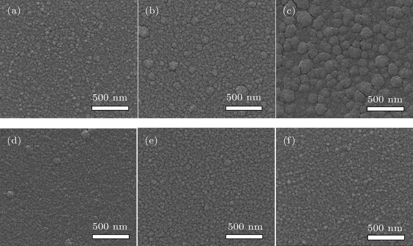
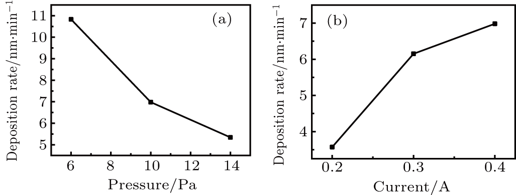
Figure 1 shows the scanning electron microscopy (SEM) top view of NiCr absorption deposited at different pressure atmospheres 4 Pa, 8 Pa, and 12 Pa in Figs. 1(a), 1(b), and 1(c), and different sputter currents 0.4 A, 0.3 A, and 0.2 A in Figs. 1(d), 1(e), and 1(f), respectively. Owing to extreme atomic shadowing effects and limited adatom diffusion, deposition at very high pressure atmosphere leads to a nanostructured and porous film; as shown in Fig. 1(c). The film deposited at low pressure atmosphere (4 Pa) has a smoother surface which produces grains between 20 nm–50 nm in diameter. If the pressure is increased to 8 Pa, then some grains with a diameter of 50 nm–100 nm are created. Using a 12-Pa pressure atmosphere produces grains with a diameter of 100 nm–200 nm all over the surface. Clearly, the general size of the grains is dependent on the pressure atmosphere. Similar evolution of grains is not found on the films deposited with different sputter currents. As shown in Figs. 1(d)–1(f), it seems that the films deposited by different sputter currents have similar grain size with a diameter of 20 nm–50 nm. It is worth noting that the deposition rate of films is decreased from 11 nm/s to 5 nm/s and from 7 nm/s to 3.5 nm/s as the pressure increases and sputter current decreases, respectively, as shown in Fig. 2. This indicates that the deposition rate is not the main reason for the formation of grains with different sizes.
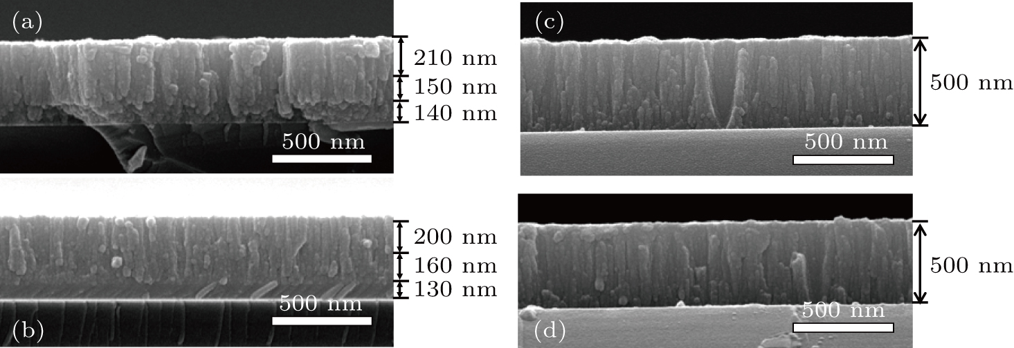
Three-layer NiCr absorbers deposited by gradient pressure and gradient current are obtained. The SEM cross-sectional views of the three-layer NiCr absorber structure deposited at an increasing pressure of 4 Pa, 8 Pa, and 12 Pa and a decreasing pressure of 12 Pa, 8 Pa, and 4 Pa are shown in Figs. 3(a) and 3(b), respectively. The thickness of these absorber films has a similar value of 500 nm. It is seen that the resulting film structure shows nano-columns with growing size. In Fig. 3(a), the nano-columns grow larger in size and the first layer on the substrate under 4 Pa shows dense column, which makes excellent adhesion properties. In contrast, the first layer in Fig. 3(b) shows oblique orientation under 12 Pa due to extreme atomic shadowing effects and limited adatom diffusion. Three-layer NiCr absorber structures deposited at an increasing current of 0.2 A, 0.3 A, and 0.4 A and a decreasing current of 0.4 A, 0.3 A, and 0.2 A are shown in Figs. 3(c) and 3(d), respectively. Similar to the trend in Figs. 1(d)–1(f), no apparent gradient layers are shown by the different current parameters.
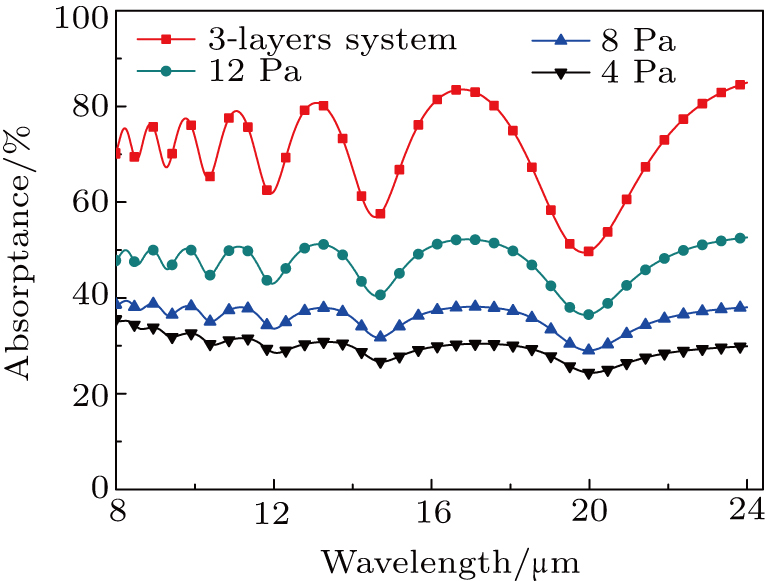
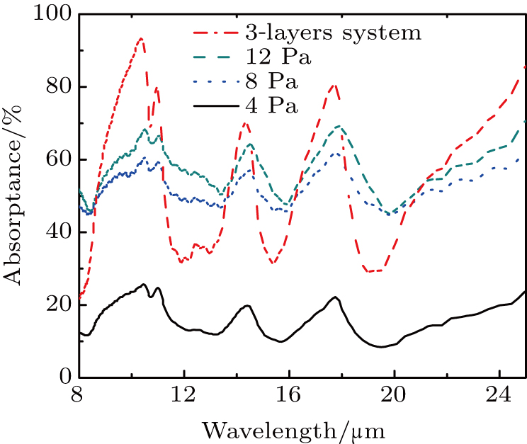
2.3. Infrared absorptionThe measured reflection curves of NiCr films produced by different argon pressures and gradient pressures with similar thickness are measured. The absorption curves are then calculated based on the relationship between reflection R and absorption A: R+A=1, because the transmission
 is equal to 0. It is clear that the absorption of NiCr films is increased at an optimal working pressure of 12 Pa (as shown in Fig. 4), while the gradient layer system shows higher absorption than single layers. The absorber features high absorption efficiency (
 ) peaks in the wavelength of
 ,
,
 , and
, and
 . The performance of the NiCr absorption layer is comparable to those metal absorption films. Schossig reported a 600-nm thick NiCr film fabricated by glancing angle deposition (GLAD) technique, which features a high absorbance of 70% in mid IR range but low absorbance of less than 50% in the wavelength of
 .[8] Shang et al. prepared a 1.5-
 thick nanostructured Cr thin-film by sputtering at a high incident angle of 110°, revealing an absorbance of 55% at
 which linearly decreases to 35% at
 .[11] The thin metal NiCr film with the thickness of less than 10 nm represents broadband absorbance radiation, while its maximum absorptivity is less than 50%.[12] Compared with these metal absorbers, the NiCr absorption layer that we proposed is more advantageous for mid/long wave infrared and very long wavelength applications such as military spacecraft. Apparently, the nano-column structure shown in SEM images (Fig. 1) on the top layer by higher argon atmosphere has a rough surface, which increases the absorption. It is known that the absorption of a metal film consists of two components: the intrinsic absorption of an ideally smooth surface and the physical structures that contributes to the enhancement of infrared absorption. In principle, the optical functionality of gradient layers can be imagined as a combination of nano-structures on the top layer and anti-reflection property induced by graded-refractive-index layers.
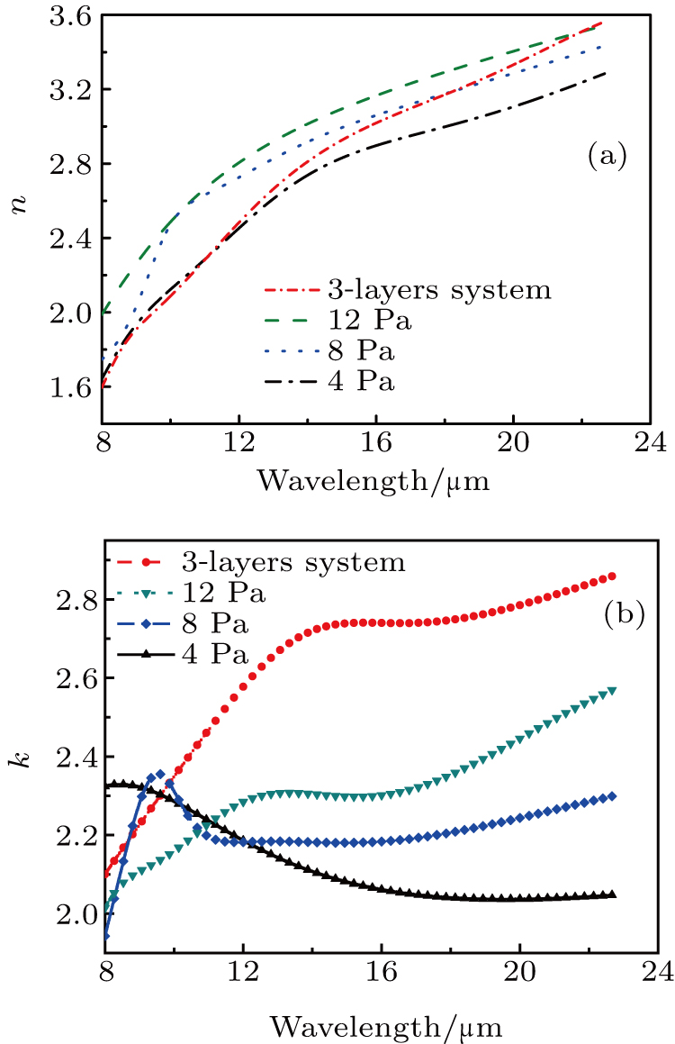
2.4. Extraction of optical parametersThe optical properties of absorbing layers can be analytically modeled based on the optical modeling proposed by Parsons et al.[13] Since the index of refraction n and extinction coefficient k are essential parameters in the simulation modeling, spectroscopic ellipsometry (SE, V-VASE ellipsometer) was used to determine these two optical constants. An ultraviolet (UV)-visible (Vis)-near-IR spectrophotometer (Cary500, Agilent) with a wavelength range of
 was used to measure the reflectance and transmittance of the samples. A simple three-phase model consisting of Ag/LiTaO3/NiCr thin films has been used to represent the sample. The variables in the fitting procedure include the layer thickness and all Tauc–Lorentz (TL) parameters. The fitting quality is poor when simple TL dispersion function is used, indicating that more than one single type of electronic transition dominates the optical absorption for NiCr films. Double TL dispersion function is then applied to fit the measured ellipsometric data in the present work. The index of refraction and the extinction coefficient as a function of wavelength can then be obtained, as shown in Fig. 5. It can be seen that the index of refraction increases as the argon atmosphere increases. NiCr with gradient layer has an average equivalent refractive index compared to that of single NiCr film with the same thickness in the wavelength range of
 . For the extinction coefficient, gradient NiCr layer has higher value than single films, which mainly contributes to the enhancement of infrared absorption.
3. Theoretical resultsEssential Macleod software is used to generate an efficient film structure design, which is a common software package for an efficient design of thin-film optical coatings. In this study, a three-layer gradient NiCr absorber and single-layer NiCr film are considered. The refractive index and extinction coefficients of NiCr absorber at different pressure atmospheres are measured using spectroscopic ellipsometry. The refraction index of LiTaO3 and Ag reflector are 2.176 and 9.5, while their extinction coefficients are 0 and 87, respectively.[14] The thicknesses of NiCr absorber, LiTaO3, and Ag reflector are 500 nm,
 , and 30 nm, respectively. The absorptance is simulated at 100 nm resolution using the Essential Macleod software, as shown in Fig. 6. The simulations are performed using the simplex parameter function of the program. Then the absorptance in the wavelength range of
 can be obtained.
It is found that the simulated absorption curves reveal a similar trend compared to the experimental measurement result. The single NiCr film exhibits an increasing absorptance as the working pressure increases, and the gradient layer system exhibits higher absorptance. Note that several absorption peaks are found at
 ,
,
 , and
, and
 , which is in good agreement with the peaks shown in measurement results. It is found that the measured absorption is relatively higher than that of simulation results. Also, a considerable deviation in the absorbance peak maximum could be observed in the wavelength range of
 , which may be caused by the measurement deviation and simulation assumption. Normally, the absorptance is provided by surface structure, as well as the optical parameters (n, k) of the materials. The trapping effect of structured surface is not considered in the simulation modeling. In principle, the three-layer gradient NiCr absorber can be imagined as a combination of anti-reflection and multiple layer cavity radiators. They can effectively remove surface reflections and, hence, increase absorption efficiency of infrared detectors.


