High quality 2-μm GaSb-based optically pumped semiconductor disk laser grown by molecular beam epitaxy
Shang Jin-Ming1, 2, Feng Jian2, 3, Yang Cheng-Ao1, 2, Xie Sheng-Wen1, 2, Zhang Yi1, 2, Tong Cun-Zhu2, 3, Zhang Yu1, 2, †, Niu Zhi-Chuan1, 2, ‡
State Key Laboratory for Superlattice and Microstructures, Institute of Semiconductors, Chinese Academy of Sciences, Beijing 100083, china
Center of Materials Science and Optoelectronics Engineering, University of Chinese Academy of Sciences, Beijing 100049, China
State Key Laboratory of Luminescence and Applications, Changchun Institute of Optics, Fine Mechanics and Physics, Chinese Academy of Sciences, Changchun 130033, China


† Corresponding author. E-mail: zhangyu@semi.ac.cn zcniu@semi.ac.cn

Project supported by the Major Program of the National Natural Science Foundation of China (Grant Nos. 61790581, 61790582, and 61790584), the National Natural Science Foundation of China (Grant No. 61435012), and the Scientific Instrument Developing Project of the Chinese Academy of Sciences (Grant No. YJKYYQ20170032).

Abstract

The epitaxial growth conditions and performance of a diode-pumped GaSb-based optically pumped semiconductor disk laser (SDL) emitting near 2.0 μm in an external cavity configuration are reported. The high quality epitaxial structure, grown on Te-doped (001) oriented GaSb substrate by molecular beam epitaxy, consists of a distributed Bragg reflector (DBR), a multi-quantum-well gain region, and a window layer. An intra-cavity SiC heat spreader was attached to the gain chip for effective thermal management. A continuous-wave output power of over 1 W operating at 2.03 μm wavelength operating near room temperature was achieved using a 3% output coupler.

1. Introduction

The mid-infrared band near 2 μm comprises a pivotal atmospheric window which includes the characteristic absorption peaks of various gases such as H2O, CO2, CH4, HF, etc. Electromagnetic waves in this band have high spatial transmittance and high light source utilization rate.[14] Therefore, some applications can be served by optoelectronic devices operating in this band, such as environmental monitoring, free space communication, biotechnology, infrared radars, material processing, etc.[57] At present, a laser operating at 2 μm can be acquired by solid-state and fiber lasers doped with Tm3+ and Ho3+ and GaSb-based laser diodes.[810] The technology of the traditional semiconductor diode laser is quite mature, and is capable of generating high power laser output efficiently and reliably. But it is difficult to obtain power greater than 1 W in a diffraction-limited circular beam due to the inherent disadvantages. A vertical cavity surface emitting laser (VCSEL) has the ability to produce an ideal circular output beam, but it is hard to achieve high power when operating in a single mode. Solid-state and fiber lasers have limitations in certain applications due to their large sizes. The emergence of an optically pumped semiconductor disk laser, first introduced by Kuznetsov et al.,[11] is expected to overcome the above shortcomings, and can realize high power and a circular near-diffraction-limited output beam.

An optically pumped semiconductor disk laser (OP-SDL), which is often referred to as vertical-external-cavity surface emitting laser (VECSEL), has been attracting considerable interest over the past decade on account of its excellent beam quality and potential high power output. The SDL, unlike traditional semiconductor lasers, combines the advantages of semiconductor lasers with those of diode-pumped solid-state lasers.[12] The SDL has a gain structure similar to that of a VCSEL. The laser output is produced by an external cavity structure, which resembles that of a solid-state laser, to produce high output power in TEM00 mode. A typical SDL cavity structure is shown in Fig. 1. Compared to solid-state and fiber lasers, the operating wavelength of an SDL can be designed utilizing semiconductor band-gap engineering, covering a wide range of practical wavelengths from visible to mid-infrared.[13,14] In addition, the absorption of pump light by the SDL is the interband transition absorption of the semiconductor material, and the absorption bandwidth is wide, which is insensitive to the drift of the pump wavelength. Due to the optical pumping, in contrast to edge-emitting semiconductor lasers or VCSELs, the SDL gain chip has no doping or ohmic contact process, which not only makes the epitaxial wafer growth simple, but also avoids free carrier absorption and Joule heat generation as well as improving the conversion efficiency of the laser. At the same time, the pumping region can be adjusted to promote the pattern matching probability provided by the external resonator and the surface-emitting geometry, near diffraction-limited and circularly symmetric output beams are generally available.[11] The external resonator structure of the SDL enables flexible control of laser characteristics by means of inserting in-cavity optical elements, such as passive mode-locking[15,16] and frequency-doubling.[17,18] These distinctive properties open up a wide range of possible applications, which have stimulated considerable interest in this type of laser.

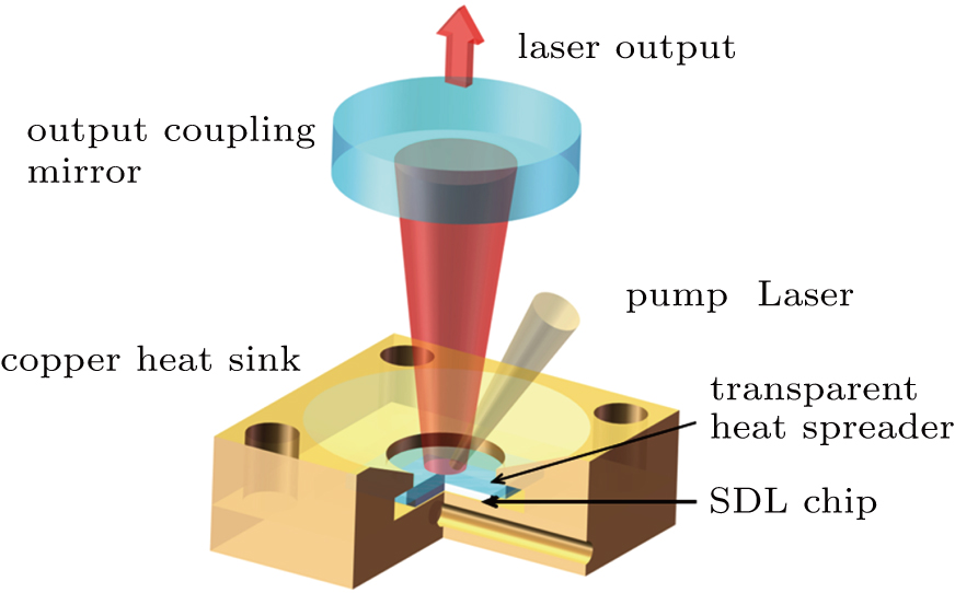
Fig. 1. Schematic of a GaSb-based SDL cavity. The semiconductor chip is sandwiched between indium foil and a transparent heat spreader to remove heat.
Fig. 2. Schematic of the SDL semiconductor layers grown by MBE.

In this paper, we present results from high quality GaSb-based SDLs with a type-I quantum well (QW) active region grown by molecular beam epitaxy. A laser power output of 1 W can be achieved at a wavelength of approximately 2.03 μm at room temperature (RT). The molecular beam epitaxial (MBE) growth and the spectral characteristics of the device are discussed.

2. Structure growth and characterization

The structures of GaSb-based SDLs were grown on Te-doped (001) oriented 2-inch GaSb substrates exploiting a VECCO Gen-II solid-source MBE system which was assembled with Sb and As cracker cells to supply group-V species. The elemental Ga, In, and Al were employed as group-III sources, which flowed over the wafer with epitaxial growth rates of 0.1–0.5 nm/s by controlling the temperature of the source furnaces. In-situ reflection high-energy electron diffraction (RHEED) was used to precisely characterize and monitor the epitaxial growth conditions and the growth temperature could be calibrated by the GaSb restructure (2 × 5 → 1 × 3) temperature at a numerical reading of 430 °C.[19]

The SDL structure is mainly composed of a highly reflective distributed Bragg reflector (DBR), a multi-quantum-well gain region, and a window layer terminated by a thin cover layer. Figure 2 exhibits the epitaxial growth structure of the GaSb-based SDL with emission wavelength of 2 μm. The DBR typically consists of 21.5 GaSb/AlAs0.09Sb0.91 quarter-wave layer pairs providing a reflectivity exceeding 99.8% at the operating wavelength. In comparison to GaAs-based SDLs that feature about 30 AlGaAs/GaAs layer pairs in general, the number of layers is significantly reduced due to the high refractive index contrast (Δn ≈ 0.7 at 2.0 μm) afforded by the III-Sb material system. The gain region typically consists of 10 layers of 10-nm-thick In0.2Ga0.8Sb quantum wells sandwiched between GaSb layers. Furthermore, to optimize the stability of growth, a double-quantum-well structure was employed in the active region design, which was placed at the antinodes of the internal standing-wave pattern to increase the modal gain. The concept of resonant periodic gain (RPG)[20] is ordinarily utilized to enhance the QW gain, which originates in the VCSEL design and subsequently is transferred to the SDL. The pump light is mainly absorbed by a barrier in typical SDL designs. To ensure higher pump absorption, the barrier layer is generally formed by a GaSb or AlGaAsSb layer that matches the growth of the GaSb substrate. The total barrier layer thickness can be significantly decreased when using GaSb as barriers of SDL structures in comparison with Al0.3Ga0.7As0.02Sb0.98 barriers. It can be seen that the GaSb barrier provides relatively high thermal conductivity and high absorption coefficient for pump wavelength. In addition, by using a GaSb barrier layer, the pump source with wavelength 1470 nm can be used to reduce the quantum defect caused by the energy difference between the pump light and the lasing light, thereby reducing heat generation and improving laser efficiency. On top of the gain region, an Al0.8Ga0.2As0.03Sb0.97 confinement layer was grown to prevent carrier nonradiative recombination, followed by a thin GaSb cap to avoid surface oxidation. The optical amplification in the SDL is derived from the type I QW in the microcavity, which is terminated by the highly reflective distributed Bragg reflector and the interface formed by the topmost semiconductor window layer and the ambient air. The scanning electron microscope (SEM) image for the gain region and the DBR is exhibited in Fig. 3. For clarity, the whole structure is divided into two parts for display and only part of the DBR layers are shown.

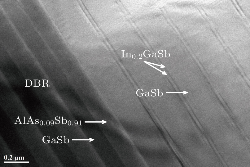
Fig. 3. SEM image of the SDL epitaxial layer. (a) Gain region and confinement region of the SDL chip. (b) DBR consisting of AlAs0.09Sb0.91 and GaSb.

After the growth of the SDL structure, the quality of the epitaxial layers is conventionally analyzed by various characterization techniques, which provide valuable information for accurate analysis of the growth parameters. The analysis of SDL structures typically includes high-resolution x-ray diffraction (HRXRD), atomic force microscopy (AFM), photoluminescence (PL) measurements, and reflectance spectroscopy. The crystal integrity and morphology of grown samples can be evaluated with the aid of HRXRD and AFM measurements. Figure 4 exhibits the HRXRD profile (004 reflection) of a 2 μm emitting SDL structure. Since there is only one main peak, it can be concluded that the barrier layer and the window layer are almost perfectly matched to the lattice of the GaSb substrate. Also the diffraction peaks generated by the compressive strain In0.2Ga0.8Sb MQW active region can also be identified. From the data shown in Fig. 4, a lattice mismatch (Δa/a0) of 1.1% is calculated for the ternary In0.2Ga0.8Sb QWs, which corresponds to a compressive strain of about 1.08%. Furthermore, the root mean square (RMS) roughness of the sample is about 0.18 nm in a 10 μm × 10 μm scan area, which indicates that the surfaces are smooth at the atomic level.

Fig. 4. Experimental HRXRD profile and an AFM image (10 μm × 10 μm) of the SDL chip.

For accurate assessment of the lattice matching and high crystalline quality during the epitaxial growth process, a cross-sectional transmission electron microscope (TEM) analysis was performed on the SDL chip (see Fig. 5). A slight dark line is clearly visible in the TEM image, which is located at the junction of the DBR and the active region due to the different growth temperature between the DBR and the active region. In addition, defects such as point defects, line defects, and surface defects were not discovered at the interface of AlAsSb and GaSb in the DBR epitaxial layer, and the growth of the double-well in the active region was perfect and no defects were found. The good structural quality of the above 2 μm SDL inferred by HRXRD was directly confirmed by cross-sectional TEM.

Fig. 5. Cross-sectional TEM micrograph of the SDL chip.

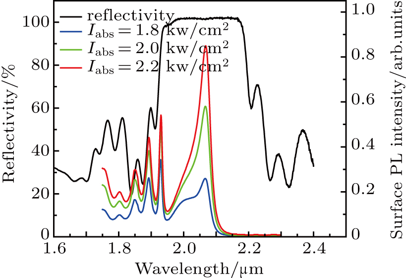
Characteristics of the SDL gain chip were assessed by PL spectrum and surface reflectivity measurements to analyze the systematic deviations in epitaxial growth of the SDL structure in advance of mounting. Reflectance spectra for GaSb-based SDL structures and surface PL spectra recorded for different pump energy densities at room temperature are shown in Fig. 6.

Fig. 6. Reflectivity and surface PL emission spectra of a 2 μm SDL structure for different pump energy densities at room temperature.

The PL curve is the result of the interaction of the microcavity formed by the DBR and the semiconductor/air interface and the emission of the quantum well structure. Within the stop band of the reflectance spectrum, a slight absorption dip is visible. The absorption dip is caused by the superposition of QW absorption and microcavity resonance. It can be clearly seen from Fig. 6 that the lasing peak position of the PL curve does not shift at different pump power densities, but the intensity of the peak alters significantly. We conclude that the temperature of the active region rises as the density of the pumping energy on the surface of the chip increases, thereby causing the PL of the QWs to drift. This drift changes the position of PL and periodic resonance gradually approaches, resulting in a significant enhancement of the emission spectrum. In addition, the maximum of the PL and the dip position in the reflectance spectra coincide with each other at a wavelength of 2060 nm. We firmly believe that the position of the surface PL is a decisive parameter for determining the resonant periodic gain (RPG) position, which is important for determining the RPG position of the SDL epitaxial design. In an SDL structure optimized for high power continuous wave (CW) operation, the QWs are designed such that the gain peak at room temperature is blue shifted tens of nanometers relative to the spectral position of the cavity resonance to achieve high power output of the device.[21] Consequently, PL and reflectivity measurements can be used as an effective quality check for the epitaxial structure prior to mounting and device operation.

3. Laser performance

The complete SDL cavity was then established by positioning a 97% reflective output coupling mirror at −50 mm from the SDL chip. The chip was optically pumped by a fiber-coupled commercial laser diode emitting at 1470 nm (Fig. 1). In order to effectively remove the thermal load of the SDL chip, a 3.0 mm × 3.0 mm chip was scribed on the wafer and bonded to a SiC heat spreader of about 400 μm in thickness by a liquid capillary,[22] which was on the top of the gain structure close to the QWs. The CW output power characteristics of the GaSb-based SDL emitting at 2 μm at different heat sink temperatures are shown in Fig. 7(a). The maximum output power of the GaSb-based SDL is slightly above 1 W when the heat sink temperature is maintained at 5 °C and the pump power is approximate 25 W. Since heat build-up affects the match between the gain peak of the device and the microcavity mode, the power drops significantly to 331 mW as the heat sink temperature rises to 15 °C. For the packaged devices, the pump absorption efficiency of the SDL chip is calculated to be less than 50% because the SiC surface as a function of the heat sink in the cavity is not subjected to coating treatment, resulting in a massive reflection loss of pump light. The normalized laser spectroscopy for different output powers at 5 °C is given in Fig. 7(b). The spectrum consists of a number of longitudinal modes centered at 2010 nm to 2035 nm. As the effective region temperature increases, the envelope of the multimode spectrum shifts to longer wavelengths as the pump power increases, thus increasing the output power.

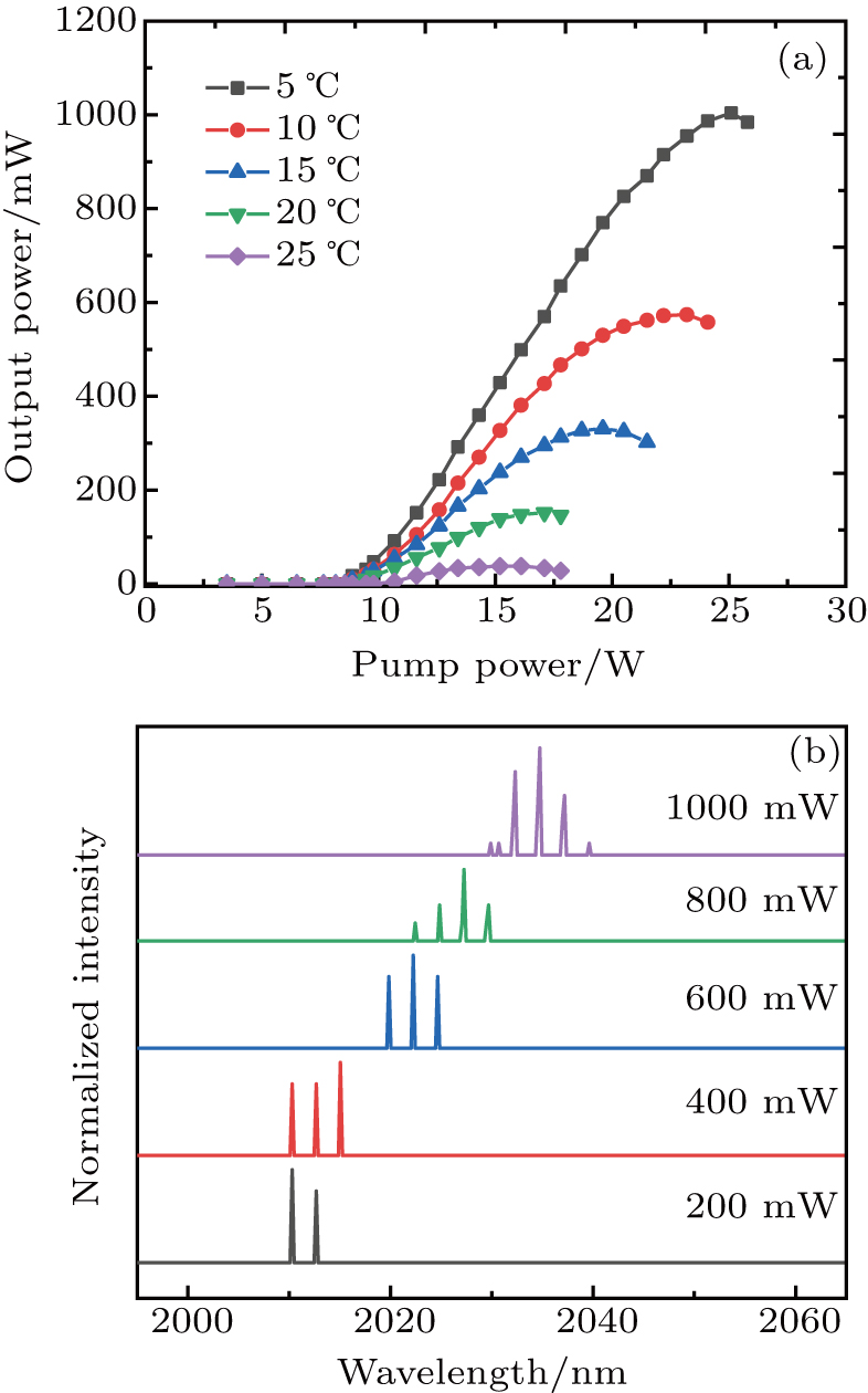
Fig. 7. (a) CW output power characteristics of a GaSb-based SDL emitting at 2 μm at different heat sink temperatures. (b) Normalized laser spectroscopy for different output powers at 5 °C.
4. Conclusion

We have demonstrated the feasibility of MBE growth of high quality GaInSb/GaSb SDL structures that achieve low quantum loss operating conditions. Using HRXRD, SEM, AFM, and TEM, we studied the surface morphology and structural characteristics of the SDL chip. The laser emission conditions of the SDL were determined by the reflection spectrum and the PL spectrum. We have also realized a GaSb-based optically pumped SDL which exhibits an outstanding output power performance near 2 μm lasing wavelength. A CW output power of 1 W was achieved at a heat sink temperature of 5 °C.

Reference
[1] Thompson A Northern H Williams B Hamilton M Ewart P 2014 Sensor. Actuat. B-Chem. 198 309
[2] Liu L Xiong B Yan Y Li J Du Z 2016 IEEE Photonic. Tech. Lett. 28 1613
[3] Curcio J A Drummeter L F Petty C C Stewart H S Butler C P 1953 Opt. Soc. Am. 43 97
[4] Luo H Yang C A Xie S W Chai X L Huang S S Zhang Y Xu Y Q Niu Z C 2018 J. Semicond. 39 104007
[5] Yang C A Zhang Y Liao Y P Xing J L Wei S H Zhang L C Xu Y Q Ni H Q Niu Z C 2016 Chin. Phys. 25 024204
[6] Krzempek K Jahjah M Lewicki R Stefański P So S Thomazy D Tittel F K 2013 Appl. Phys. 112 461
[7] Von E M Scheuermann J Nahle L Zimmermann C Hildebrandt L Fischer M Koeth J Weih R Hofling S Kamp M 2014 Proc. SPIE 8993 89318
[8] Baranov A N Cuminal Y Boissier G Nicolas J C Lazzari J L Alibert C Joullié A 1996 Semiconduct. Sci. Technol. 11 1185
[9] DeLoach L D Page R H Wilke G D Payne S A Krupke W F 1996 IEEE J. Quantum. Elect. 32 885
[10] Mirov S B Fedorov V V Moskalev I S Martyshkin D V Myoung N Camata R Williams J E Mirov M S Goldstein J T 2011 Opt. Mater. 1 898
[11] Kuznetsov M Hakimi F Sprague R Mooradian A 1997 IEEE Photon. Technol. Lett. 9 1063
[12] Shu S L Hou G Y Feng J Wang L J Tian S C Tong C Z Wang L J 2018 Opto-Elecreon. Adv. 1 170003
[13] Rudin B Rutz A Hoffmann M Maas D J H C Bellancourt A R Gini E Keller U 2008 Opt. Lett. 33 2719
[14] Rahim M Arnold M Felder F Behfar K Zogg H 2007 Appl. Phys. Lett. 91 151102
[15] Keller U Tropper A C 2006 Phys. Rep. 429 67
[16] Lorenser D Maas D J H C Unold H J Bellancourt A R Rudin B Gini E Keller U 2006 IEEE J. Quantum. Elect. 42 838
[17] Chilla J L A Butterworth S D Zeitschel A Charles J P Caprara A L Reed M K Spinelli L 2004 Proc. SPIE 5332 143
[18] Gerster E Ecker I Lorch S Hahn C Menzel S Unger P 2003 Appl. Phys. 94 7397
[19] Xing J L Zhang Y Xu Y Q Wang G W Wang J Xiang W Ni H Q Ren Z W He Z H Niu Z C 2014 Chin. Phys. 23 017805
[20] Corzine S W Geels R S Scott J W Yan R H Coldren L A 1989 IEEE J. Quantum. Elect 25 1513
[21] Schulz N Rattunde M Ritzenthaler C Rosener B Manz C Kohler K Wagner J 2007 IEEE Photonic. Tech. 19 1741
[22] Liau Z L 2000 Appl. Phys. Lett. 77 651