


Photodetectors based on inorganic halide perovskites: Materials and devices
Cite this Article
Li Ying, Shi Zhi-Feng, Li Xin-Jian, Shan Chong-Xin. Photodetectors based on inorganic halide perovskites: Materials and devices. Chinese Physics B, 2019, 28(1): 017803 
Permissions
Photodetectors based on inorganic halide perovskites: Materials and devices
† Corresponding author. E-mail:
Abstract
The newly emerging metal halide perovskites have attracted considerable attention due to their exceptional optoelectronic properties. This upsurge was initially driven when the power conversion efficiency of perovskite-based photovoltaic devices exceeded 23%. Due to their optoelectronic properties, perovskite materials have also been used in light-emitting diodes, photodetectors, lasers, and memory devices. This study comprehensively discusses the recent progress of all-inorganic perovskite-based photodetectors, focusing on their structures, morphologies of their constituent materials, and diverse device architectures that improve the performance metrics of these photodetectors. A brief outlook, highlighting the main existing problems, possible solutions to these problems, and future development directions, is also provided herein.
1. Introduction
Photodetectors that convert incident optical signals to electrical signals are crucial in a broad range of applications, including medial analysis, security surveillance, optical communications, and biological sensing.[1–5] Commercialization prospects are high for photodetectors with good responsivity, fast response speed, low power consumption, good stability, and low processing cost. Among the various semiconductor materials explored for light detection, the newly emerging organic–inorganic hybrid perovskites (CH3NH3PbX
3, X = Cl, Br, and I) have triggered considerable attention[6–16] probably owing to their excellent properties such as tunable bandgap, high and well-balanced electron/hole mobility, large carrier diffusion length, and low-temperature processing technique.[4,17–21] At present, most of the studied photodetectors are based on conventional semiconductors, such as graphene, two-dimensional (2D) materials, and silicon, which are expensive and require precise preparation techniques. In contrast, metal halide perovskite-based photodetectors can be fabricated with high crystallinity via solution processing at low temperatures. In addition, the device performances of perovskite photodetectors have rapidly improved over the past three years. The responsivity and specific detectivity of perovskite photodetectors can reach 109 A/W and 

This study summarizes the recent achievements in all-inorganic halide perovskite-based photodetectors, including Pb-based and lead-free photodetectors. The structural feature of halide perovskites and their various synthesis methods are introduced first. Then, all-inorganic perovskite photodetectors with metal–semiconductor–metal and heterojunction structures are reviewed. Finally, this review concludes with a summary and a positive outlook on the future development of perovskite photodetectors.
2. Structural features and synthesis of all-inorganic perovskites
2.1. Structural features
Inorganic metal halide perovskites are chemically represented as ABX
3, where A is an inorganic cation (e.g., Cs), B denotes the metal cation (e.g., Pb, Sn), and X is a halide anion (Cl, Br, and I).[37] A typical perovskite crystal has a cubic (α phase) unit cell (Fig.
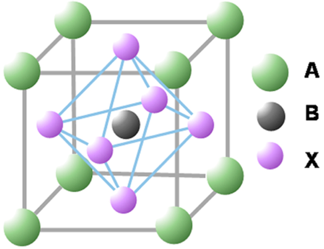 | Fig. 1. General crystal structure of perovskites ABX 3.[37] |
Compared with organic–inorganic hybrid perovskites, all-inorganic perovskites have received less attention, although their properties are comparable to those of organometallic perovskites. Both these materials are imbued with a direct bandgap, tunable emission wavelength, high light absorption coefficient (up to 105 cm−1), simple processing technique, as well as high and well-balanced carrier-transport ability. Regarding the tunable bandgap, perovskite photodetectors are considered as broadband detectors, enabling full-band coverage of the ultraviolet and visible light regions. The bandgap of perovskites can be tuned by varying the composition of the constituent halide ions and/or cations without changing the electronic properties of the perovskites. In the past few years, compositional tunability has been extensively studied in perovskite materials.[26,38,39]
2.2. Synthesis of all-inorganic perovskites
In optoelectronic devices, metal halide perovskites are mainly applied as light absorbers. Devices with excellent optoelectronic properties require high-quality perovskites, regardless of their shape and dimensions. Several synthetic methods for synthesizing halide perovskites have proliferated and they are now divisible into three main categories.
2.2.1. Solution-processed synthesis
As a simple and low-cost synthesis method, one-step spin coating is commonly used to prepare perovskites with different morphologies, such as films, nanowires, nanoplatelets, and single crystals. Figure
 | Fig. 2. Solvent engineering procedure for fabricating uniform and dense perovskite films.[40] |
The solution process yields perovskite thin films, as well as high-quality nano- and micro-structures such as CsPbCl3 nanocrystals.[45] Liu et al. reported all-inorganic photodetectors based on solution-processed scattered CsPbBr3 nanoplatelets. The nanoplatelets were highly oriented, with an average lateral dimension as large as 

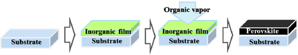
2.2.2. Vapor-assisted solution process
Chen et al. exploited the separate advantages of vapor and solution processes and developed a hybrid technique, known as the vapor-assisted solution process, for solar cell applications. In this method, a PbI2 layer deposited by spin coating is subsequently treated with the desired CH3NH3I vapor (Fig.
 | Fig. 4. Schematic of the vapor-assisted solution process.[48] |
2.2.3. Vapor deposition
Vapor-phase synthesis is suitable for growing epitaxial nanostructures of inorganic perovskites with improved crystal quality because crystals grown using this method are thermally stable at moderately high temperatures.[55–57] Figure
 | Fig. 5. Schematic of the vapor deposition process.[58] |
At present, solution-processed synthesis, vapor-assisted solution process, and vapor deposition are all widely and successfully employed in perovskite preparation. Among these three methods, solution-processed synthesis is low-cost, easier to operate, and obtains a high-quality perovskite layer at relatively low temperatures. The vapor-assisted solution process is more complicated compared with the solution method but is suitable for materials that do not easily dissolve in solvents. Vapor-phase synthesis obtains epitaxial perovskite micro/nanostructures with high crystal quality. Moreover, the dimensions and thicknesses of crystals grown using this method are easily controlled.
2.2.4. Hot-injection approach
Perovskite photodetectors can be fabricated using a quantum dots (QDs) solution prepared via the hot-injection method. Following the traditional hot-injection approach, which is a common synthesis method of metal chalcogenide QDs, Kovalenko et al. synthesized the first monodispersed CsPbX 3 QDs with a high degree of compositional bandgap engineering.[26] Therein, the Cs precursors were injected into the lead–halide precursors containing hot solvents with high boiling points. A mixture of oleic acid and oleylamine dissolved the lead–halide sources and stabilized the QDs. In situ PL measurements revealed a very fast reaction process after the Cs precursor injection. Most CsPbX 3 QDs were synthesized within a few seconds. In such a rapid synthesis method, the unit size of the CsPbX 3 QDs strongly depends on the reaction temperature and is reduced by decreasing the reaction temperature. In that study, the CsPbX 3 QDs were produced with a tunable size of 4–15 nm.
3. Lead–halide perovskite photodetectors
3.1. Parameters of photodetectors
where I
d is the dark current, P
opt is the incident light intensity, and S is the effective illuminated area. R reflects the photoelectric conversion capability of the photocurrent.
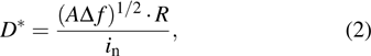
where A is the effective area of the detector, Δ f is the electrical bandwidth, and i
n is the noise current. When the dark current is dominated by shot noise, D
* is represented as follows:
where I
d is the dark current. Clearly, the dark current should be reduced as far as possible to distinguish very weak optical signals.
where e is the elementary charge, h and c are the Planckʼs constant and light speed, respectively, and ν and λ denote the frequency and wavelength of the incident light, respectively.
where I
p is the photocurrent measured at a light intensity of 1 mW/cm2 and I
d is the dark current.
Photodetectors are evaluated using several important parameters, such as responsivity (R), detectivity (D *), external quantum efficiency (EQE), response time, and linear dynamic range (LDR), which are briefly described as follows:

 |
 |
 |
 |
 |
3.2. Metal–semiconductor–metal (MSM) photodetector
The sensitivity of organic–inorganic halide perovskites to oxygen exposure and damp conditions destabilizes the corresponding devices; therefore, all-inorganic lead halide perovskites, chemically represented by CsPbX
3 (X = I, Br, and Cl), have received considerable research attention. The simplest configuration for CsPbX
3 photodetector fabrication is metal–semiconductor–metal (MSM), which sandwiches the perovskite absorber between two contact electrodes. This structure is widely adopted in perovskites photodetectors.[67–71] Li et al. fabricated prototypical CsPbBr3 thin-film photodetectors with a coplanar MSM interdigitated patterned Au-electrode configuration. The CsPbBr3 thin film was prepared using one-step spin coating (Fig. 
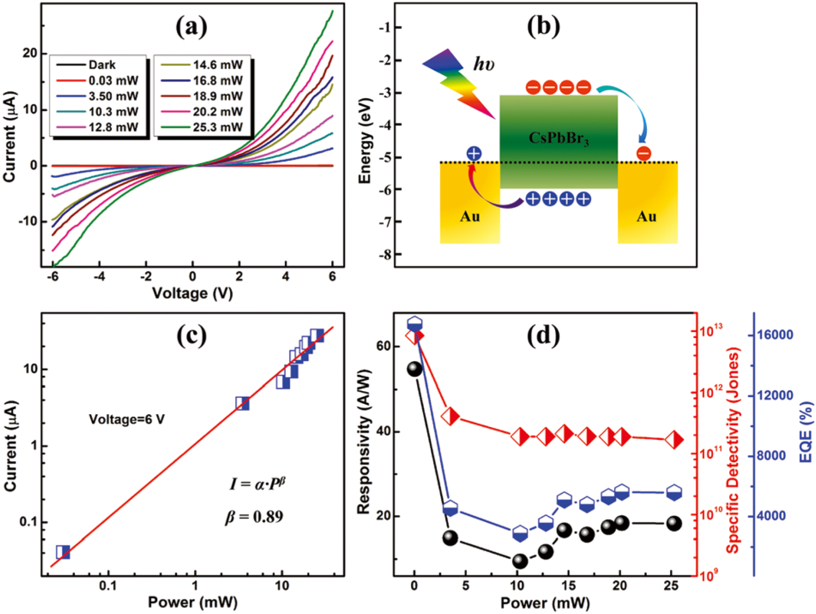 | Fig. 6. (a) Current–voltage (I–V) characteristics of the studied photodetector illuminated by light at different power densities. (b) Energy band diagrams of the Au/CsPbBr3/Au structure showing the generation, transfer, and collection processes of the photogenerated carriers. (c) Logarithmic plot of the photocurrent versus illumination power. The curve is well fitted using a power law. (d) Photoresponsivity (blck), specific detectivity (red), and EQE (blue) of the photodetectors versus the illuminated light irradiance.[41] |
Further improvements in the detector performance of thin-film systems are limited by many factors, such as the large grain boundaries in polycrystalline structures and the low EQE due to the short lifetime of the photogenerated carriers. Therefore, the research focus has shifted toward nano- and micro-structures of perovskites, which are fabricated with fewer grain boundaries, lower defect/trap density, smaller recombination rate, and longer lifetime of the photogenerated carriers compared with thin films.[45,46,55,67–73] Tang et al. demonstrated an MSM photodetector based on CsPb(Br/I)3 nanorods. The device was fabricated by placing toluene-dissolved nanorods in a gold interdigital electrode on a SiO2 substrate with 3-
 | Fig. 7. (a) Schematic of the photodetector based on CsPbCl3 microwire networks. (b) Normalized photocurrent of the non-encapsulated CsPbCl3 microwire-network photodetectors over time. The operation continued for 9 h at 373 K.[69] |
Zhang et al. fabricated ultraviolet photodetectors based on cubic CsPbCl3 nanocrystals. The configuration was a typical indium tin oxide (ITO)/CsPbCl3 nanocrytals/quartz stack. First, a 100-nm-thick CsPbCl3 nanocrystal film was fabricated via spin coating. Next, a pair of interdigitated ITO electrodes (100-nm thick) was thermally evaporated onto the films using a shadow mask, forming a 200-nm-wide and 5-

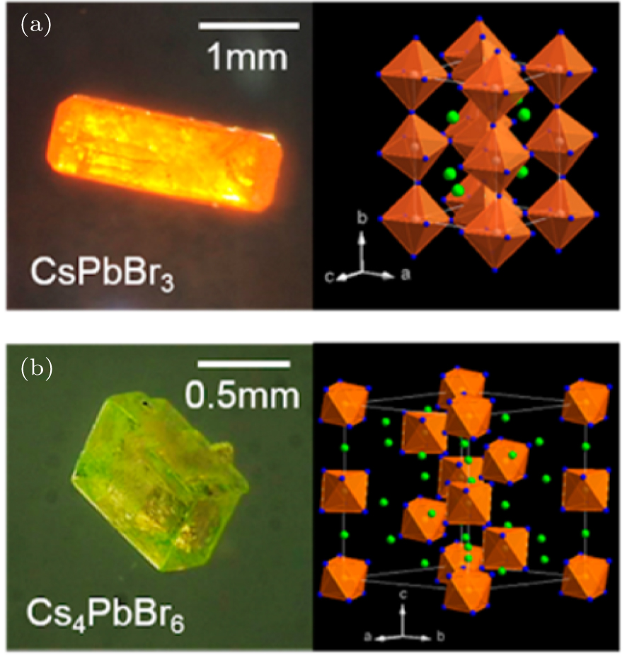
Photodetectors based on single-perovskite single crystals have also been prepared. After determining the appropriate growth conditions, Cha et al. fabricated millimeter-sized CsPbBr3 and Cs4PbBr6 crystals using the anti-solvent vapor-assisted crystallization method in polar solvents at room temperature. Panels (a) and (b) of Fig.
 | Fig. 8. Optical microscopy images and crystal structure diagrams of (a) CsPbBr3 and (b) Cs4PbBr6 crystals (orange octahedrons, [PbBr6]4−; green dots, Cs atoms; blue dots, Br atoms).[70] |
The aforementioned results typify the characteristics of an MSM photodetector, namely large photocurrent, high responsivity, and slow response time. Therefore, many researchers have sought ways to improve the performance of photodetectors. For instance, Song et al. fabricated two-dimensional (2D) nanosheets of CsPbBr3 and incorporated them into a high-performance photodetector. The structure of this device is presented in Fig. 


 | Fig. 9. (a) Configuration schematic of the device based on CsPbBr3 nanosheets. (b) High-magnification SEM images of the device. (c) I–V characteristics of the photodetector in the dark and under irradiation with 442-nm light (0.35 mW/cm2). Inset: working principle of the photodetector. (d) Normalized high-resolution photoresponse, showing the rise and decay times.[72] |
Pang et al. demonstrated a CsPbBr3 photodetector based on high-quality, well-aligned nanoribbons, confirming that 6,6-phenyl-C61-butyric acid ethyl ester (PCBM) not only passivates the defects on the CsPbBr3 nanoribbon surface but also transfers the charge. Figure
 | Fig. 10. (a) Logarithmic I–V curves of the photodetector devices under light illumination (504 nm, 10 mW/cm2) and in darkness. (b) Time-resolved photocurrents in the photodetectors based on bare CsPbBr3 nanoribbon film and in PCBM passivated CsPbBr3 nanoribbon film.[73] |
More recently, Tong et al. applied dual-phase inorganic perovskites (CsPbBr3–CsPb2Br5) as the light-harvesting layer in photodetectors. The dual-phase perovskites were synthesized using the physical vapor deposition method on rigid and flexible substrates. More specifically, CsBr and PbBr2 films were sequentially deposited on the substrates via thermal evaporation, controlling the PbBr2 excess by regulating the thickness. The deposition was followed by a post-annealing step in air at 13 °C to form the dual-phase inorganic perovskites. The halogen ions (Br−) were enriched on the surfaces of the inorganic perovskite films, enabling a wide-bandgap semiconductor of CsPb2Br5 in the film and a consequent self-passivation phenomenon on the interface, which might reduce the charge recombination at the interface. The inset of Fig. 

 | Fig. 11. (a) Ultraviolet–visible absorbance spectrum of inorganic dual-phase perovskite film; inset: photographs of the inorganic perovskite film on glass substrate under ambient conditions (left) and under ultraviolet illumination (right). The films are sized 2.5 ×1.5 cm2. (b) Corresponding magnified and normalized plots of one response cycle for estimating the rise and fall times of the photodetector.[76] |
3.3. Heterojunction photodetectors
The planar MSM structure is the typical architecture of perovskite photodetectors. However, because the device lacks an efficient charge-blocking layer or a built-in field, the dark-noise current is high and the response speed is slow, limiting further improvements of the detection limit. To overcome the drawbacks of the MSM structure, heterojunction photodetectors have been extensively studied. Bao et al. processed high-performance heterojunction photodetectors from all-inorganic CsPbIxBr3−x thin films (Fig.
 | Fig. 12. (a) Schematic of the structure of the photodetector based on all-inorganic perovskites CsPbIxBr3−x. (b, c) I–V curves of the CsPbIBr2- and CsPbBr3-based photodetectors in the dark and under illumination with 450-nm monochromatic light of different intensities (
|
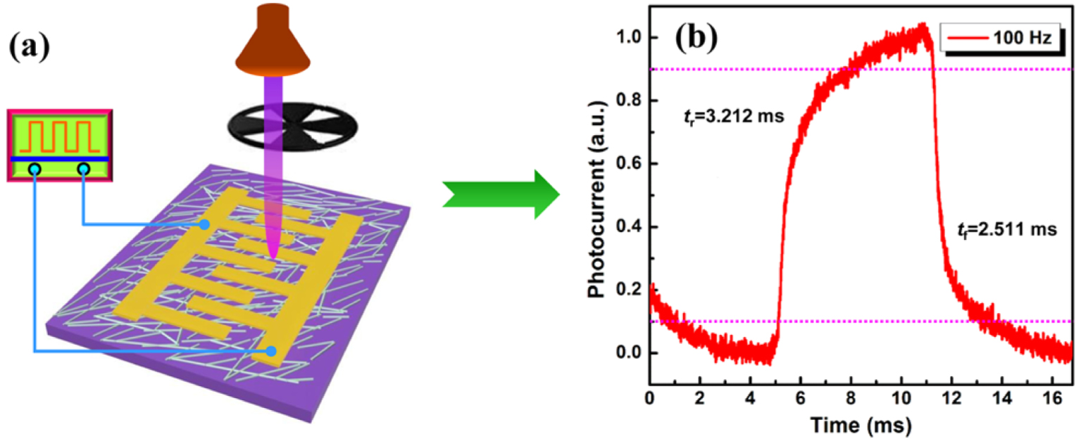
Lu et al. recently proposed a new hybrid 3D architecture that integrates inorganic perovskite QDs with high quantum yield on hydrogenated amorphous silicon (a-Si:H) radial junctions (RJs) constructed over silicon nanowires (SiNWs). This architecture demonstrated an ultrafast and efficient optoelectronic down-conversion for solar-blind ultraviolet detection. Figure
 | Fig. 13. (a) Schematic of the multilayered a-Si thin-film PIN RJ structure constructed on SiNWs. (b) Magnified and normalized plots of one response cycle showing the rise and fall times.[78] |
Zhou et al. fabricated self-powered all-inorganic CsPbBr3 perovskites for microcrystal photodetectors with high detectivity and a fast response time. Threrein, CsPbBr3 perovskite microcrystals were prepared directly on SnO2-coated substrates using a modified inverse temperature crystallization method. The resulting microcrystals were 

 | Fig. 14. (a) Energy band diagram of the CsPbBr3 microcrystal perovskite photodetector. (b) Rising and falling edges for estimating rise and fall times of the photodetector at 500 Hz.[79] |
Song et al. proposed a novel photodetector structure based on a ZnO hollow ball/CsPbBr3 heterojunction. The ZnO hollow balls function as an ultraviolet response center, and the CsPbBr3 is designed as a green light-emitting material. The CsPbBr3 perovskites shield the ZnO from air contact and allow the smooth passage of the photogenerated holes to GaN. Owing to the superior ultraviolet-light trapping characteristics of the device, the ultraviolet light response is huge, with an on/off ratio and specific detectivity of 16527 and 2.4 ×10¹³ Jones, respectively. Similar to Lu et al.ʼs device,[26] the proposed photodetector operates accurately without requiring an external power supply. The CsPbBr3 insertion improved the dual-functional performance from that of the traditional ZnO/GaN structure at various wavelengths. This improvement was conferred by the better contact interface and the green-light emission center. The ZnO/CsPbBr3/GaN structure yielded much higher values than the ZnO/GaN structure, and its response region was widened to 550 nm, except in the ultraviolet region. Additionally, the ZnO/CsPbBr3/GaN structure displayed a blue electroluminescence under a low-threshold voltage. By separating the light-responsive and actively emitting regions, this structure avoids the contradictory principles of carrier transport, possibly enabling high-performance dual-functional devices.[80]
4. Lead-free halide perovskite photodetectors
Despite the remarkable progress of high-performance perovskite photodetectors constructed from lead–halide absorbers APbX
3, the toxicity of lead remains a concern in the large-scale applications of these photodetectors. Substituting lead (Pb) with bivalent tin (Sn) might resolve the toxicity problem. Recently, CsSnX
3 perovskite (X = Cl, Cl0.5Br0.5, Br, Br0.5I0.5, and I)[81,82] and Cs2SnI6 perovskite derivatives have been synthesized via a facile hot-injection process.[83] However, most of these materials are used in light-emitting diodes, laser, and solar cells.[84–90] Photodetector applications of lead-free halide perovskites, particularly all-inorganic Sn-based perovskites, are scarce. Sb-based perovskites are another promising alternative. Cs3Sb2X
9 (X = Cl, Br, and I) QDs have been fabricated via solution-phase synthesis and applied in luminescent devices and solar cells.[91–94] Pradhan et al. synthesized Cs3Sb2Cl9 nanocrystals by employing a colloidal synthesis route. Guided by their experimental observations, they modeled the atomic arrangements of the trigonal and orthorhombic phases in the nanowires. In both phases, the Cs and Cl atoms showed a close-packed arrangement with the Sb atoms (Figs.
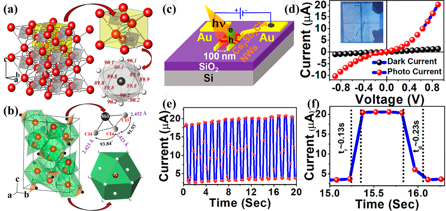 | Fig. 15. (a) Atomic arrangements of the trigonal phase of Cs3Sb2Cl9 nanowires: unit cell (top) and SbCl6 octahedra (bottom). (b) Atomic arrangements of the orthorhombic phase: irregular triangular planar geometry of Sb and Cl (top) and polyhedron (bottom). Black, red, and white spheres correspond to Sb, Cs, and Cl, respectively. (c) Schematic of the photodetector device. (d) Current versus voltage characteristics of the Cs3Sb2Cl9 nanowires under dark and light-illuminated conditions. Inset is an optical image of the device. (e) Photo-switching behavior at 0.9 V, revealing fast on/off switching states with a time interval of 500 ms. (f) Rise and decay times of a single on/off cycle.[95] |
All-inorganic Bi-based perovskites have also been successfully synthesized.[96–102] Tong et al. developed a sensitive red-light photodetector based on CsBi3I10 perovskite thin films fabricated via spin coating. In an optoelectronic study, the as-assembled device demonstrated obvious sensitivity to red-light illumination, excellent reproducibility, and good spectral selectivity. Figure 
 | Fig. 16. Stepwise fabrication process of the CsBi3I10 perovskite film-based photodetector.[43] |
The heterovalent substitution concept, in which a pair of Pb(II) ions is replaced by a monovalent B+ and a trivalent B3+ ion to form an A2B+B3+X
6 double-perovskite structure, has also attracted considerable attention. Cs2AgBiBr6 is regarded as a highly promising replacement of conventional lead halides.[102–104] Lei et al. fabricated lead-free perovskite photodetectors with the light absorbers of double-perovskite Cs2AgBiBr6 thin film synthesized using the one-step spin coating. The reaction sources were high-purity CsBr, AgBr, and BiBr3. To investigate the potential applications of such Cs2AgBiBr6 thin films in photoelectric response, Lei et al. constructed a photoconductive detector with a coplanar MSM interdigitated patterned Au-electrode configuration. Figure 
 | Fig. 17. (a) Energy band diagram of the Au/Cs2AgBiBr6/Au structure, showing the generation, transfer, and collection processes of the photogenerated carriers. (b) Spectral responses of the Cs2AgBiBr6 thin-film photodetector. (c) I–V curves of the photodetector under light with different illumination powers. (d) Logarithmic plot of photocurrent versus illumination power. (e) Photoresponsivity and (f) specific detectivity and EQE of the photodetector versus light illumination power.[105] |
Recently, Wu et al. reported a self-powered photodetector based on the ITO/SnO2/Cs2AgBiBr6/Au structure but without a hole-transport layer. The device is self-powered with two responsivity peaks at 350 and 435 nm, suitable for light detection within 320–400 nm and deep-blue light, respectively. Owing to the high integrity of Cs2AgBiBr6 thin film and the efficient interface charge transfer from perovskite to the underlying SnO2, the photodetector demonstrated a high responsivity of 0.11 A/W at 350 nm and a quick response time of 
Table 
| Table 1.
Summary of all-inorganic perovskite-based photodetectors. . |
5. Conclusions
Owing to the unprecedented optoelectronic properties of halide perovskite-based solar cells, perovskite photodetectors have considerably progressed over the past few years. This study has comprehensively overviewed the recent advances in all-inorganic halide perovskite materials and photodetectors with different device structures, including lead-based and lead-free halide perovskites. Recent reports on lead-free perovskite photodetectors were also discussed. The reported environmentally friendly alternatives are desired in practical applications. However, many unsolved problems remain and the stability and performance of halide perovskite-based devices require further development. It is hoped that this study will promote research on all-inorganic perovskite photodetectors, securing their practical applicability in the foreseeable future.
Reference
| [1] | |
| [2] | |
| [3] | |
| [4] | |
| [5] | |
| [6] | |
| [7] | |
| [8] | |
| [9] | |
| [10] | |
| [11] | |
| [12] | |
| [13] | |
| [14] | |
| [15] | |
| [16] | |
| [17] | |
| [18] | |
| [19] | |
| [20] | |
| [21] | |
| [22] | |
| [23] | |
| [24] | |
| [25] | |
| [26] | |
| [27] | |
| [28] | |
| [29] | |
| [30] | |
| [31] | |
| [32] | |
| [33] | |
| [34] | |
| [35] | |
| [36] | |
| [37] | |
| [38] | |
| [39] | |
| [40] | |
| [41] | |
| [42] | |
| [43] | |
| [44] | |
| [45] | |
| [46] | |
| [47] | |
| [48] | |
| [49] | |
| [50] | |
| [51] | |
| [52] | |
| [53] | |
| [54] | |
| [55] | |
| [56] | |
| [57] | |
| [58] | |
| [59] | |
| [60] | |
| [61] | |
| [62] | |
| [63] | |
| [64] | |
| [65] | |
| [66] | |
| [67] | |
| [68] | |
| [69] | |
| [70] | |
| [71] | |
| [72] | |
| [73] | |
| [74] | |
| [75] | |
| [76] | |
| [77] | |
| [78] | |
| [79] | |
| [80] | |
| [81] | |
| [82] | |
| [83] | |
| [84] | |
| [85] | |
| [86] | |
| [87] | |
| [88] | |
| [89] | |
| [90] | |
| [91] | |
| [92] | |
| [93] | |
| [94] | |
| [95] | |
| [96] | |
| [97] | |
| [98] | |
| [99] | |
| [100] | |
| [101] | |
| [102] | |
| [103] | |
| [104] | |
| [105] | |
| [106] | |
| [107] | |
| [108] | |
| [109] | |
| [110] | |
| [111] | |
| [112] | |
| [113] | |
| [114] | |
| [115] | |
| [116] |