Physical manipulation of ultrathin-film optical interference for super absorption and two-dimensional heterojunction photoconversion
Cao Guo-Yang1, 2, Zhang Cheng1, 2, Wu Shao-Long1, 2, Ma Dong3, †, Li Xiao-Feng1, 2, ‡
School of Optoelectronic Science and Engineering & Collaborative Innovation Center of Suzhou Nano Science and Technology Soochow University, Suzhou 215006, China
Key Laboratory of Advanced Optical Manufacturing Technologies of Jiangsu Province, Key Laboratory of Modern Optical Technologies of the Education Ministry of China, Soochow University, Suzhou 215006, China
School of Rail Transportation, Soochow University, Suzhou 215131, China


† Corresponding author. E-mail: madong@suda.edu.cn xfli@suda.edu.cn

Project supported by the National Natural Science Foundation of China (Grant Nos. 61675142 and 61875143), the Natural Science Foundation of Jiangsu Province, China (Grant No. BK20140359), the Natural Science Research Project of the Higher Educational Institutions of Jiangsu Province, China (Grant No. 17KJA480004), the Postgraduate Research & Practice Innovation Program of Jiangsu Province, China (Grant No. KYCX17 2027), and the Priority Academic Program Development of the Higher Educational Institutions of Jiangsu Province, China.

Abstract

Ultrathin optical interference in a system composed of absorbing material and metal reflector has attracted extensive attention due to its potential application in realizing highly efficient optical absorption by using extremely thin semiconductor material. In this paper, we study the physics behind the high absorption of ultrathin film from the viewpoint of destructive interference and admittance matching, particularly addressing the phase evolution by light propagation and interface reflection. The physical manipulations of the ultrathin interference effect by controlling the substrate material and semiconductor material/thickness are examined. We introduce typical two-dimensional materials — i.e., MoS2 and WSe2 — as the absorbing layer with thickness below 10 nm, which exhibits ∼ 90% absorption in a large range of incident angle (0° ∼ 70°). According to the ultrathin interference mechanism, we propose the ultrathin (< 20 nm) MoS2/WSe2 heterojunction for photovoltaic application and carefully examine the detailed optoelectronic responses by coupled multiphysics simulation. By comparing the same cells on SiO2 substrate, both the short-circuit current density (up to 20 mA/cm2) and the photoelectric conversion efficiency (up to 9.5%) are found to be increased by ∼ 200%.

1. Introduction

Highly efficient optical absorption plays a fundamental role in a broad range of optoelectronic applications, including photoelectric conversion (e.g., photodetection and photovoltaics),[1,2] photochemical cells,[3,4] light emission,[5,6] sensing,[7] etc. A photon-harvesting device without a good absorption can hardly obtain a high performance, no matter how the electrical conversion is optimized. Unfortunately, highly absorbing materials are always highly impedance-mismatched with air, leading to high reflection by the device surface.[8] Strengthened optical absorption can be achieved by employing the photonic designs. The most conventional strategy is to introduce single layer or multi-layer antireflection (AR) coatings composed of lossless dielectrics.[9] However, the AR layers need a quarter-wavelength in thickness, which hinders the miniaturizing of the optoelectronic devices (especially for infrared or far-infrared devices). Recently, with the rapid progress of nanofabrication technologies, the deep-subwavelength systems with broadband and high absorption (e.g., those that are based on plasmonics or metamaterials) have been extensively studied and demonstrated.[1014] Nevertheless, such systems largely rely on the precisely nanopatterning one or several layers, which require costly and complicated fabrication, thus hindering them from being used on a large-scale and lowing their cost in application.

Recently, a simple and ingenious solution based on anti-reflection principle was proposed to realize a broadband, wide-angle, and ultrahigh absorption in the ultrathin film with 10 nm–20 nm in thickness (far less than the quarter-wave thickness).[9,1518] In the solution, 1) light-absorbing semiconductor replaces the conventional lossless dielectric material and 2) metal is used as back reflector. The special combination of highly absorbing semiconductor and metal reflector can greatly reduce the AR thickness because the reflection phase-shift introduced by the semiconductor/metal interface is significantly increased so that the required phase variation through the semiconductor becomes substantially small, allowing a much smaller thickness of the material. The unique thin-film planar scenario enables an extremely high absorption in the ultrathin semiconductor film. For example, Kats (Park) et al. reported that the 15 (12) nm Ge film on Au (Ag) substrate can absorb over 80% (98%) of light at a wavelength of λ ∼ 670 (625) nm.[9,16] Such a planar system has also various applications, e.g., in ultrathin color coatings,[9] broadband solar energy harvesting,[1,19] ultrathin devices based on van der Waals semiconductors,[15] etc. It has been indicated that the material and dimension of the metal and the semiconductor are critical for the ultrathin system to achieve high optical performance. Moreover, various deep-subwavelength film/metal systems under the same AR condition exhibit very distinguished optical absorbing performances. Therefore, more details of the fundamental optics within the ultrathin devices are required if we wish to better control the light coupling with the materials. In addition, the applications of this new system need to be further explored. For example, for the ultrathin solar cells, it is necessary to combine the superior optical performance with the realistic carrier transport/recombination process so that the complete optoelectronic performance of the device can be evaluated for a better device design.

In this paper, we first investigate the underlying optical mechanism responsible for the high absorption of the ultrathin semiconductor film on metal substrate, particularly addressing the phase evolution with the interface reflection and internal propagation, and also quantifying the phase condition for the destructive interference. The optical performances of the system under various semiconductor materials, semiconductor material thicknesses, and substrate materials are systematically studied. Moreover, an ideal substrate enables the system to possess the better absorption performance of the system than the systems under realistic metal or dielectric substrates. The scheme is further applied to a two-dimensional (2D) system with typical 2D materials, i.e. MoS2 and WSe2, which exhibits nearly perfect absorption and good angular dependence with a material thickness below 10 nm. Finally, we design the ultrathin MoS2/WSe2 heterojunction for photovoltaic application with carefully examining the detailed optoelectronic responses, such as external-quantum efficiency (EQE) and current–voltage (JV) curve. Compared with the same solar cell on conventional SiO2 substrate, the short-circuit current density (Jsc) and photoelectric conversion efficiency (PCE) are both improved by ∼ 200%. The strong ultrathin-film interference provides the possibility of realizing miniaturized planar systems for high-performance, low-cost, and large-scale optoelectronic applications.

2. Device and method

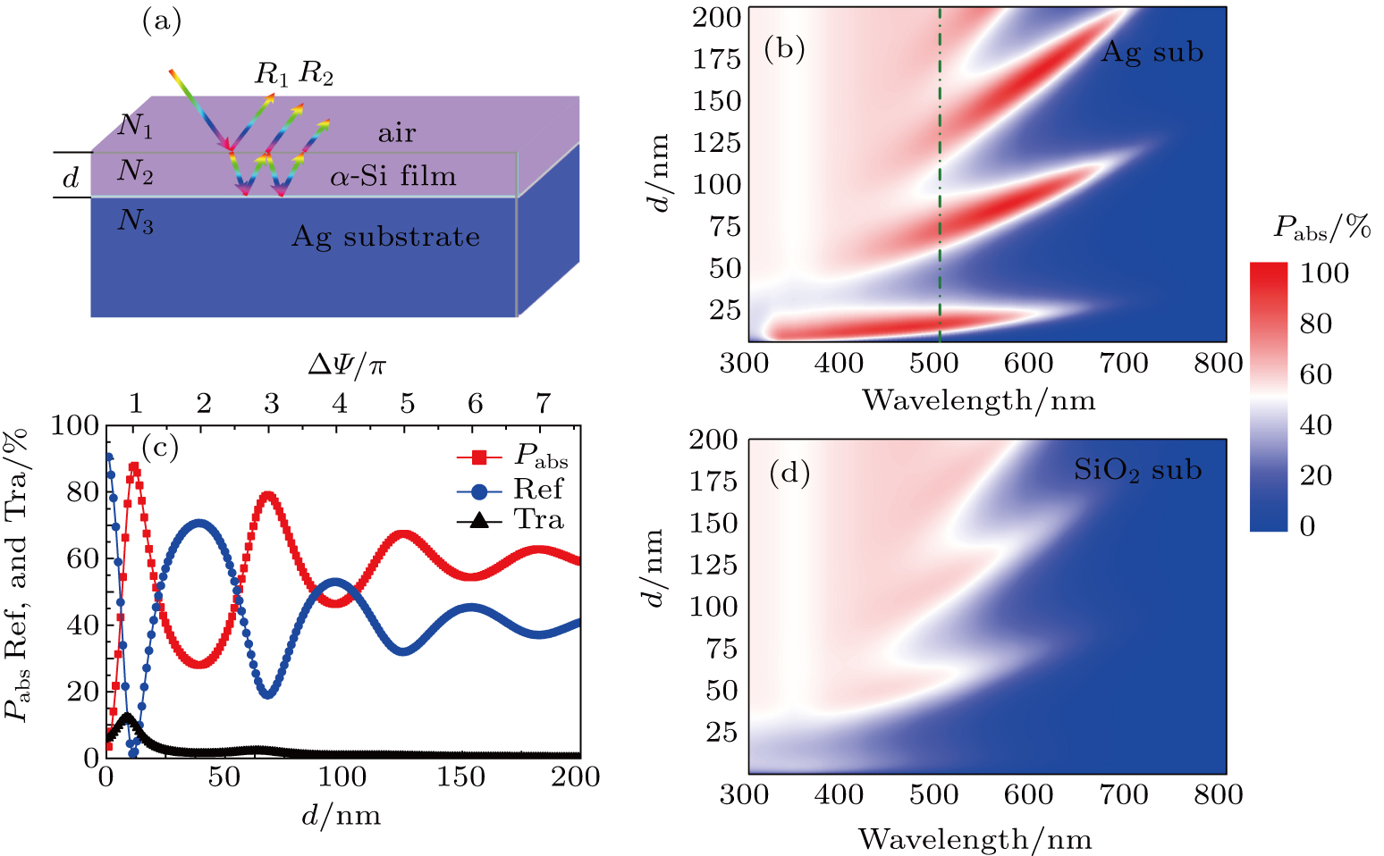
A sketch of the ultrathin multilayer system is shown in Fig. 1(a), where N1 (= n1 = 1), N2 (= n2 + ik2) and N3 (= n3+ik3) are the complex refractive index of Air, α-Si, and Ag, respectively, and d is the thickness of the α-Si film. Initially, the α-Si film is considered as the absorbing AR layer on Ag (more material options to be determined later). Since the Ag layer is thick enough (much larger than the skin-depth of light in Ag), the substrate below Ag can be ignored; therefore, we refer to the Ag (or other metals) on the top of substrate as the Ag-substrate (or other metals) system. Considering that the light is perpendicularly incident onto the film from air, the optical response of the device is investigated by the Fresnel formula and transfer matrix method (TMM). The optical parameters of the materials under consideration are cited from the Palik table.[20]

Fig. 1. (color online) (a) Sketch of device, where N1, N2, and N3 are refraction indexes of air, α-Si, and Ag substrates, respectively. Pabs versus wavelength and α-Si thickness d on (b) Ag and (d) SiO2 substrate under perpendicular incidence. (c) absorption, reflection, and transmission of the ultrathin film system versus d with λ = 500 nm. The top-x-axis shows corresponding ΔΨ.

We first briefly introduce the calculation process for studying the special optical interference in the ultrathin dielectric/metal system. The reflection coefficient and phase shift in the air/film (film/Ag) interface are denoted as r12 (r23) and Ψ12 (Ψ23), respectively, the phase accumulation in the thin film is represented by Ψd, and the phase difference between the direct surface reflection (R1) and the reflected light by film/Ag after a round-trip propagation through the film (R2) is denoted as ΔΨ (without considering the high-order components). The phase change by interface reflection can be calculated by Fresnel formula. Note that the phase relation just considers the first-order propagation wave inside the ultrathin system. Given that the high-order components show dramatically reduced intensity, this treatment can approximate to the actual antireflection condition. Then we utilize TMM to calculate the optical response of the ultrathin system, including absorption (Pabs), reflection (Ref), and transmission (Tra). The admittance of air, film, and substrate are η1, η2, and η3, respectively. Note that the free space admittance (y0) is taken to be the unit of admittance. The unpolarized sunlight absorption is modelled by the average of light absorptions under transverse-electric (TE, s-polarized) and transverse-magnetic (TM, p-polarized) incidence. The equivalent admittance of the whole system is ηz. The admittance difference between air and the system (i.e., η1 and ηz) is denoted as Δη.

3. Results and discussions

Figures 1(b) and 1(d) show the profiles of Pabs of the ultrathin α-Si film versus λ and d on Ag and SiO2 substrates, respectively. It is obvious that: 1) both systems exhibit several absorption bands in the dispersion diagrams due to the excitation of various modes under destructive interference, and 2) the d value and the peak λ have a nearly linear relation, which can be explained by calculation formula of Ψd. Moreover, the thinner absorbing layer leads the wider-band absorption to increase, which is beneficial to the design of many photoconversion devices such as the solar cells.[1,2] If we compare the results of the two systems based on Ag and SiO2 substrates, the peaked absorption in the Ag system (Fig. 1(b)) is substantially higher than that of the SiO2 system (Fig. 1(d)) due to the ultrathin optical interference effect as mentioned in the literature.[1517]

At λ = 500 nm, the α-Si Pabs, Ref, and Tra of the ultrathin α-Si/Ag system versus d are plotted in Fig. 1(c), where ΔΨ is given to justify the interference situation. On the whole, Pabs and Ref oscillate with d in a contrary way and the absorption peaks (reflection dips) occur when ΔΨ = (2M + 1)π (M = 0, 1, 2,…);i.e., the destructive interference between the directly reflected light and the first order propagation light in the AR layer. Further study shows that the peaked Pabs decreases gradually with increasing d (i.e., enlarging the order number m), which can be explained by the higher admittance mismatch Δη between air and the system (see Table 1), weakening the AR effect despite the fact that the destructive phase condition is preserved. This suggests that the AR phase matching is not a sufficient condition for ultrahigh absorption because the admittance matching is also an important ingredient. In addition, the Ag substrate as a back reflector plays also a key role in enhancing absorption by efficiently restraining the transmission and elongating the light-path in the ultrathin film.

Table 1.

Values of d, ΔΨ, and Δη at M = 0, 1, 2, and 3.

.

Figure 1(c) indicates that the Pabs peak of α-Si material at d of only 12 nm can reaches up to 90%. Such an outstanding light-trapping ability by an ultrathin semiconductor is due to the following reasons: 1) the phase change by the reflection of α-Si/Ag (air/α-Si) interface is 1.63π (1.02π); therefore, the phase accumulation in the α-Si layer is only 0.39π to satisfy the AR phase condition, allowing thickness to be very small—far less than the quarter wavelength; 2) there is a good admittance matching between the incident medium and the structure, and 3) Ag substrate reduces dramatically the transmission and enhances light-path in the ultrathin α-Si film.

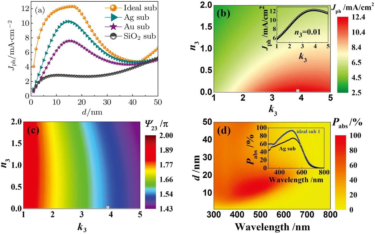
Actually, for such an ultrathin system, the choice of back reflector is critical because it strongly affects the optical interference on the top surface. Moreover, as mentioned in Fig. 1, the ultrathin system can be used to achieve the broadband optical absorption; therefore, in the following, we introduce the AM1.5G solar illumination and evaluate the overall system performance by using the spectrally integrated photocurrent density Jph.[21] With an assumption of a perfect internal quantum process, which means that photo-generated carriers transform completely into output current, the photocurrent density Jph can be calculated from , where λ1 (λ2) is the starting (cutoff) wavelength, q the electron charge, and FS the spectral photon flux density of AM1.5G. Figure 2(a) shows the plots of Jph versus d under ideal, Ag, Au, and SiO2 substrate. Here, the ideal substrate is obtained by sweeping real and imaginary part of the substrate refractive index (N3 = n3 + ik3) at each thickness of α-Si layer. It is obvious that as a broadband absorber, the system with SiO2 substrate shows fundamentally lower Jph, since the phase variation within the ultrathin α-Si layer is insufficient for AR interference. The Ag and Au substrates enable the AR effect to achieve much higher Jph and comparably the Ag system can obtain the peak Jph > 10 mA/cm2 at d = 15 nm; i.e., a surprisingly high photocurrent by such an ultrathin semiconductor. Nevertheless, the existing metals do not provide the best optical performance. It can be seen from Fig. 2(a) that the system with an optimized substrate can exhibit a Jph > 12 mA/cm2 with d = 16 nm.

Fig. 2. (color online) (a) Plots of Jph versus d on various substrates. (b) Plot of Jph versus N3 (= n3 + ik3) with d = 16 nm, where inset shows plot of Jph versus k3 with n3 = 0.01. (c) Reflection phase (Ψ23) by the film/substrate interface. (d) Plots of Pabs versus d and wavelength with Ideal sub 1 (Nsub = 0.01+3.9i), where the inset shows plot of Pabs spectrum of system (with d = 16 nm) on Ideal sub 1 and Ag, respectively.

To achieve a high Jph, figure 2(b) reveals that n3 has to be sufficiently small and k3 has to be appropriately designed (see the inset of Fig. 2(b), where Jph versus k3 is shown with n3 = 0.01). It suggests that the ideal N3 = 0.01+3.9i (denoted as Ideal sub 1 here). Correspondingly, figure 2(c) shows the map of the reflection phase change by the α-Si/substrate interface (i.e., Ψ23) at λ = 500 nm. Our calculation indicates that Ψ23 = 1.54π and, therefore, ΔΨ ∼ 1.08π when using the Ideal sub 1, approximately satisfies the AR phase matching. There is a tiny difference from the calculated ΔΨ (1.08 π) in the ideal situation (π) since the design is for the full solar-spectrum absorption rather than the single AR wavelength. Figure 2(d) displays the Pabs spectrum of the α-Si film on Ideal sub 1 versus d, where the Pabs spectra at d = 16 nm with Ag and ideal substrates are compared in the inset. It is clear that the absorption ability of the ultrathin α-Si film on Ideal sub 1 is superior to that on the Ag substrate in a wide waveband.

However, with the α-Si thickness decreasing into nanosize, the defect density of the ultrathin film becomes dramatically high[15] and this seriously limits the photoelectric conversion performance (despite the fact that the optical performance has been optimized significantly). Therefore, it is necessary to replace the conventional semiconductor material by the high-quality 2D materials; for instance, MoS2, WSe2, and other transition metal dichalcogenides layered materials (TMDLM). These 2D materials show many outstanding properties:[2225] 1) no surface dangling bond, thus reducing the carrier loss caused by surface recombination, 2) strong light-absorbing ability [light is absorbed by the single layer MoS2 (0.65 nm) is approximate to that of 50-nm-thick Si], and 3) reasonable and tunable bandgap by controlling the number of layers. In Fig. 3, we continually modulate the real and imaginary part of the refractive index of the AR material, i.e., N2 = n2 + ik2, and examine the absorption performances at a representative wavelength of 500 nm on various substrates (Ideal sub 2, Ag, Au, and Cu). Here, the thickness of the AR layer is d = 9 nm and the Ideal sub 2 (with N3 = 0.01+1.36i) is designed by sweeping n3 and k3 under the given system configuration (similar to Fig. 2(b)). In these patterns, we can identify the materials of MoS2, WSe2, and α-Si according to their refractive index. It is found that the systems under Ideal sub 2 and Ag substrate show higher absorptions than those under the Au and Cu substrates. With Ideal sub 2 (Ag substrate), WSe2 (MoS2) system shows nearly unity absorption. The Pabs values under various AR and substrate materials are listed in Table 2.
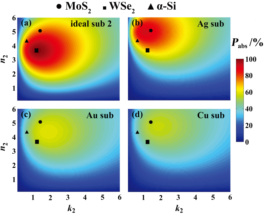
Fig. 3. (color online) Pabs versus N2 (= n2 + ik2) when d = 9 nm and λ = 500 nm respectively on (a) Ideal sub 2 (Nsub = 0.01 + 1.36i), (b) Ag, (c) Au, and (d) Cu substrate.
Table 2.

Pabs values under various film and substrate configurations, with film thickness d = 9 nm and perpendicular light wavelength 500 nm.

.

By simultaneously modulating the film and substrate, it is found that even thinner film can obtain ultrahigh absorption. Figure 4(b) shows that 1-nm-thick ideal film on a designed substrate with N3 = 0.01+0.01i can achieve Pabs = 99% under perpendicular incidence at the wavelength of 500 nm. Figure 4 also displays the corresponding Ref, ΔΨ, and Δη. It is shown that the reflection dip, absorption peak, phase relation under antireflection, and the admittance match happen at an identical N2. Moreover, figure 4(c) indicates that there are many options for antireflection phase condition; however, the system does not show the corresponding high absorption or low reflection, indicating that the phase matching is just a necessary but not sufficient condition for antireflection effect.
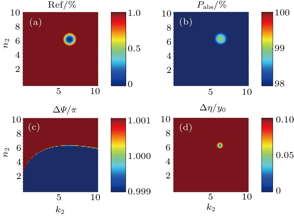
Fig. 4. (color online) Ref, Pabs, ΔΨ, and Δη of 1 nm of film versus N2 on ideal substrate (N3 = 0.01+0.01i) with 500 nm of perpendicular incidence.

Since the material is extremely thin, the angular performance is expected to be much higher than the angular performance of the conventional AR system.[19] Here, the TE and TM light incidence are taken into account and their average is used to mimic the non-polarized sunlight illumination. Figure 5 exhibits the angular response of Pabs of MoS2 and WSe2 ultrathin film with d = 9 nm and λ = 500 nm on Ideal sub 2 (Figs. 5(a) and 5(b)) and Ag substrate (Figs. 5(c) and 5(d)). From the figure, the Pabs value of MoS2 and WSe2 ultrathin film keep sufficiently high within a broad range of incident angle (0°–70°). This is because the phase responsible for the destructive interference comes mostly from the semiconductor/metal interface, rather than from the wave propagation in the AR layer; therefore, the AR effect can be roughly satisfied under different incident angles. The performance will be dramatically degraded only when the incident angle is sufficiently large (∼ 80°) due to the obvious phase mismatch.
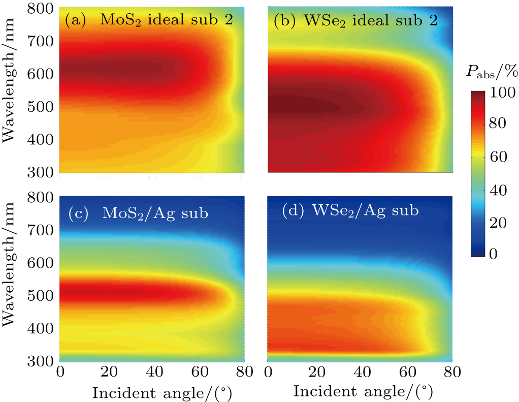
Fig. 5. (color online) Angular response of Pabs of MoS2 and WSe2 ultrathin film with d = 9 nm on (a) and (b) Ideal sub 2 and (c) and (d) Ag substrates.

Figure 5 also shows that the MoS2 (WSe2) ultrathin films absorb mainly the long (short) wavelength light; therefore, we can design the MoS2/WSe2 heterojunction ultrathin solar cell as an interesting application of the deep-subwavelength AR effect. When considering the solar cells, the detailed carrier dynamics during the generation, recombination, and collection in the device must be taken into account in order to evaluate the photoelectric performance accurately. The coupled optoelectronic simulation has been introduced to study various photoelectric devices in our previous research.[21,2629] Here, we show the fundamental equations of the semiconductor model: where Dn (Dp) is the electron (hole) diffusion coefficient, μn (μp) the electron (hole) mobility, n (p) the electron (hole) concentration, NC (NV) the effective conduction (valence) band density of states, χ the electron affinity, χ the electrostatic potential, T (300 K) the operating temperature, kB the Boltmann’s constant, Eg the band gap, ε0 (εr) the vacuum permittivity (relative permittivity of the material), ND (NA) the donors (acceptors) concentration, and G(x, y, ε ) the carrier generation distribution, U the recombination. In the proposed heterojunction system comprised of 2D materials, the surface recombination can be ignored due to the absence of the surface dangling bond;[25] the bulk and interface recombinations include the contributions from Langevin and Shockley–Read–Hall (SRH) mechanisms.[26] Here we solve the Maxwell’s equations, electron/hole transport equations, and Poisson’s equation by the finite-element method (FEM) and finite-volume method (FVM) in COMSOL Multiphysics to obtain the photoelectric performance of the ultra-thin MoS2/WSe2 heterojunction solar cell.[26] Since no high-dimensional nanopatterns are used in this system, the simulation can be performed by 2D models. The thickness of the multilayer MoS2 and WSe2 are 9.8 nm and 8.64 nm, respectively, and the key material parameters used in the simulation are cited from the literature.[24,26,3041]

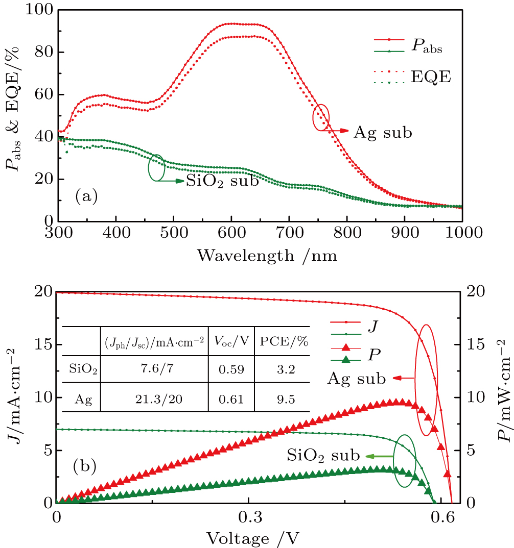
Figure 6(a) displays the Pabs and EQE spectra of the ultrathin MoS2/WSe2 heterojunction solar cells on Ag and SiO2 substrates. It is clear that the improved optical response under the ultrathin interference effect is well transferred into the electrical domain, showing much higher EQE than the EQE of the conventional system with SiO2 substrate. It should be mentioned that the ultrathin interference effect here is designed for the AR dual-layers, showing that the new optical scheme is applicable for the multilayer systems. Figure 6(b) shows the corresponding JV curves under the two system configurations. Moreover, the optoelectronic performance parameters are inserted into the figure, in which the PCE = (Pmax/Pin) ×/%, where Pmax (= JV) is the maximal output power density and Pin (≈ 100 mW/cm2) is the input power of AM1.5 solar illumination. These parameters include Jph, Jsc, open-circuit voltage (Voc), and PCE, which are 21.3 (7.6) mA/cm2, 20 (7.0) mA/cm2, 0.61 (0.59) V, and 9.5% (3.2%), respectively, for the proposed heterojunction solar cell on Ag (SiO2) substrate. It is obvious that the photocurrent densities and the PCE are enhanced by almost 200% by utilizing the ultrathin interference effect. Interestingly, the heterojunction system with thickness less than 20 nm is predicted to show a PCE of 9.5%, which could be an opportunity for ultrathin high-performance photoconversion devices.

Fig. 6. (color online) (a) Pabs and EQE spectra of MoS2/WSe2 ultrathin heterojunction solar cell on Ag and SiO2 substrates. (b) Corresponding JV characteristics and output power density (P), where the typical performance parameters are inserted.
4. Conclusions

We have presented a comprehensive study on the ultrathin-film interference effect of the system, which is composed of strongly absorbing dielectric and back metal reflector, from the underlying physics, photonic manipulation, optical performance optimization, and also the photoconversion application. The transfer-matrix treatment, impedance matching condition, and the antireflection effect are used/discussed in detail. The various geometry and material options of the absorbing dielectric and substrate are considered through a comparable study of the system optical performance. It is found that the phase matching of antireflection is necessary but not a sufficient condition for ultrahigh absorption because the admittance matching is also an inevitable requirement. Particular attention is also paid to the incorporating of the 2D materials into this ultrathin-film system, which shows very good optical absorption in a large range of the incident angle. Finally, we construct an ultrathin MoS2/WSe2 heterojunction system for photovoltaic application. Under an AM1.5 solar illumination, the short-circuit current density, open-circuit voltage, and light-conversion efficiency of the proposed heterojunction on Ag (SiO2) sub are 20 (7.0) mA/cm2, 0.61 (0.59) V, and 9.5% (3.2%), respectively. Compared with the conventional system with dielectric substrate, the dielectric/metal setup shows the photocurrent density and PCE to be enhanced by ∼ 200%, thus promoting the practical application of TMDLM in photoelectric conversion.

Reference
[1] Piper J R Fan S 2016 ACS Photon. 3 571
[2] Pala R A White J Barnard E Liu J Brongersma M L 2009 Adv. Mater. 21 3504
[3] Hasobe T Fukuzumi S Kamat P V 2006 J. Phys. Chem. 110 25477
[4] Lebedev N Trammell S A Dressick W Kedziora G S Griva I Schnur J M 2011 Photochem. Photobiol. 87 1024
[5] Yeh D M Huang C F Chen C Y Lu Y C Yang C C 2008 Nanotechnol. 19 345201
[6] Sun G Khurgin J B Soref R A 2008 J. Opt. Soc. Am. 25 1748
[7] Kano H Kawata S 1994 Appl. Opt. 33 5166
[8] Rensberg J Zhou Y Richter S Wan C Zhang S Schöppe P SchmidtGrund R Ramanathan S Capasso F Kats M A Ronning C 2017 Phys. Rev. Appl. 8 014009
[9] Kats M A Blanchard R Genevet P Capasso F 2013 Nat. Mater. 12 20
[10] Yu N Capasso F 2014 Nat. Mater. 13 139
[11] Yao Y Shankar R Kats M A Song Y Kong J Loncar M Capasso F 2014 Nano Lett. 14 6526
[12] Fang Z Liu Z Wang Y Ajayan P M Nordlander P Halas N J 2012 Nano Lett. 12 3808
[13] Echtermeyer T J Britnell L Jasnos P K Lombardo A Gorbachev R V Grigorenko A N Geim A K Ferrari A C Novoselov K S 2011 Nat. Commun. 2 458
[14] Gilbertson A M Francescato Y Roschuk T Shautsova V Chen Y Sidiropoulos T P Hong M Giannini V Maier S A Cohen L F Oulton R F 2015 Nano Lett. 15 3458
[15] Jariwala D Davoyan A R Tagliabue G Sherrott M C Wong J Atwater H A 2016 Nano Lett. 16 5482
[16] Park J Kang J H Vasudev A P Schoen D T Kim H Hasman E Brongersma M L 2014 ACS Photon. 1 812
[17] Kats M A Sharma D Lin J Genevet P Blanchard R Yang Z Qazilbash M M Basov D N Ramanathan S Capasso F 2012 Appl. Phys. Lett. 101 221101
[18] Luo J Li S Hou B Lai Y 2014 Phys. Rev. 90 165128
[19] Liu D Yu H Duan Y Li Q Xuan Y 2016 Sci. Rep. 6 32515
[20] Palik E D 1985 Handbook of Optical Constants of Solids San Deigo Academic Press USA 571 586
[21] Cao G Li X Zhan Y Wu S Shang A Zhang C Yang Z Zhai X 2014 Opt. Express 22 A1761
[22] Wi S Kim H Chen M Nam H Guo L Meyhofer E Liang X 2014 ACS Nano 8 5270
[23] Yin Z Li H Li H Jiang L Shi Y Sun Y Lu G Zhang Q Chen X Zhang H 2011 ACS Nano 6 74
[24] Radisavljevic B Radenovic A Brivio J Giacometti I V Kis A 2011 Nat. Nanotechnol. 6 147
[25] Lee C H Lee G H Van Der Zande A M Chen W Li Y Han M Cui X Arefe G Nuckolls C Heinz T Guo J Hone J Kim P 2014 Nat. Nanotechnol. 9 676
[26] Cao G Shang A Zhang C Gong Y Li S Bao Q Li X 2016 Nano Energy 30 260
[27] Shang A Zhai X Zhang C Zhan Y Wu S Li X 2015 Prog. Photovolt.: Res. Appl. 23 1734
[28] Li X Zhan Y Wang C 2015 Prog. Photovolt.: Res. Appl. 23 628
[29] Li X Hylton N P Giannini V Lee K H EkinsDaukes N J Maier S A 2013 Prog. Photovolt.: Res. Appl. 21 109
[30] Eichfeld S M Eichfeld C M Lin Y C Hossain L Robinson J A 2014 APL Mater. 2 092508
[31] Yim C O'Brien M McEvoy N Winters S Mirza I Lunney J G Duesberg G S 2014 Appl. Phys. Lett. 104 103114
[32] Liu H L Shen C C Su S H Hsu C L Li M Y Li L J 2014 Appl. Phys. Lett. 105 201905
[33] Bao W Cai X Kim D Sridhara K Fuhrer M S 2013 Appl. Phys. Lett. 102 042104
[34] Das S Chen H Y Penumatcha A V Appenzeller J 2012 Nano Lett. 13 100
[35] Fang H Chuang S Chang T C Takei K Takahashi T Javey A 2012 Nano Lett. 12 3788
[36] Cui X Lee G H Kim Y D Arefe G Huang P Y Lee C H Chenet D A Zhang X Wang L Ye F Pizzocchero F Jessen B S Watanabe K Taniguchi T Muller D A Low T Kimv P Hone J 2015 Nat. Nanotechnol. 10 534
[37] Liu W Kang J Sarkar D Khatami Y Jena D Banerjee K 2013 Nano Lett. 13 1983
[38] Furchi M M Pospischil A Libisch F Burgdörfer J Mueller T 2014 Nano Lett. 14 4785
[39] Britnell L Ribeiro R M Eckmann A Jalil R Belle B D Mishchenko A Kim Y J Gorbachev R V Georgiou T Morozov S V Grigorenko A N Geim A K Casiraghi C Castro Neto A H Novoselov K S 2013 Science 340 1311
[40] Zhou S Ye Y Ding K Jiang D Dou X Sun B 2018 Chin. Phys. Lett. 35 066201
[41] Kadir N A A Ismail E I Latiff A A Ahmad H Arof H Harun S W 2017 Chin. Phys. Lett. 34 014202