Physical manipulation of ultrathin-film optical interference for super absorption and two-dimensional heterojunction photoconversion
Project supported by the National Natural Science Foundation of China (Grant Nos. 61675142 and 61875143), the Natural Science Foundation of Jiangsu Province, China (Grant No. BK20140359), the Natural Science Research Project of the Higher Educational Institutions of Jiangsu Province, China (Grant No. 17KJA480004), the Postgraduate Research & Practice Innovation Program of Jiangsu Province, China (Grant No. KYCX17 2027), and the Priority Academic Program Development of the Higher Educational Institutions of Jiangsu Province, China.
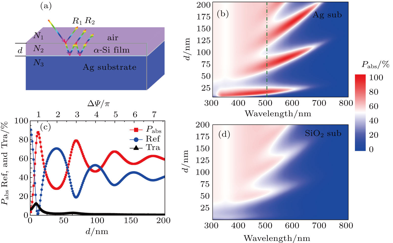
(color online) (a) Sketch of device, where N1, N2, and N3 are refraction indexes of air, α-Si, and Ag substrates, respectively. Pabs versus wavelength and α-Si thickness d on (b) Ag and (d) SiO2 substrate under perpendicular incidence. (c) absorption, reflection, and transmission of the ultrathin film system versus d with λ = 500 nm. The top-x-axis shows corresponding ΔΨ.
